EP1246292A2 - Zweiweg-Isolator und Verfahren zu seiner Beurteilung - Google Patents
Zweiweg-Isolator und Verfahren zu seiner Beurteilung Download PDFInfo
- Publication number
- EP1246292A2 EP1246292A2 EP02007190A EP02007190A EP1246292A2 EP 1246292 A2 EP1246292 A2 EP 1246292A2 EP 02007190 A EP02007190 A EP 02007190A EP 02007190 A EP02007190 A EP 02007190A EP 1246292 A2 EP1246292 A2 EP 1246292A2
- Authority
- EP
- European Patent Office
- Prior art keywords
- ferrite plate
- thin ferrite
- input
- output terminal
- port isolator
- Prior art date
- Legal status (The legal status is an assumption and is not a legal conclusion. Google has not performed a legal analysis and makes no representation as to the accuracy of the status listed.)
- Withdrawn
Links
Images


Classifications
-
- H—ELECTRICITY
- H01—ELECTRIC ELEMENTS
- H01P—WAVEGUIDES; RESONATORS, LINES, OR OTHER DEVICES OF THE WAVEGUIDE TYPE
- H01P1/00—Auxiliary devices
- H01P1/32—Non-reciprocal transmission devices
-
- H—ELECTRICITY
- H01—ELECTRIC ELEMENTS
- H01P—WAVEGUIDES; RESONATORS, LINES, OR OTHER DEVICES OF THE WAVEGUIDE TYPE
- H01P1/00—Auxiliary devices
- H01P1/32—Non-reciprocal transmission devices
- H01P1/36—Isolators
Definitions
- the present invention relates to a two-port isolator having large isolation and small insertion loss in a wide bandwidth, and a method for evaluating it.
- the circulator has a basic structure comprising a thin ferrite plate, a permanent magnet for applying a magnetic field to the thin ferrite plate perpendicularly, and conductors disposed around the thin ferrite plate, with irreversible electric characteristics.
- the distributed element is used when the size of the thin. ferrite plate is 1/4 or more of the wavelength of a high-frequency signal transmitting therethrough.
- the lumped element circulator is used when the size of the thin ferrite plate is 1/8 or less of the wavelength of a high-frequency signal transmitting therethrough. Accordingly, the lumped element circulator is more suitable for miniaturization than the distributed element circulator.
- Fig. 7 is a schematic view showing an isolator circuit used for cell phones, etc. at present, which is constituted by connecting a matching impedance (resistor R) to one port of the three-port, lumped element circulator.
- Three central conductors L 1 , L 2 , L 3 are disposed at an equal interval of 120° on the upper surface of a thin ferrite plate G composed of garnet-type ferrite.
- One end of each central conductor L 1 , L 2 , L 3 serves as an input-output line for a terminal (1), (2), (3), and the other end is connected to a common terminal GR serving as a ground.
- Matching capacitors C 1 , C 2 , C 3 are parallel-connected between the ends of the central conductors L 1 , L 2 , L 3 and the common terminal GR.
- an energy-absorbing resistor R is connected between the terminal (3) and the common terminal GR.
- a permanent magnet (not shown) is mounted onto a casing serving as a magnetic yoke.
- a center frequency f 0
- a high-frequency signal entering into the terminal (1) is transmitted to the terminal (2)
- a high-frequency signal entering into the terminal (2) is transmitted to the terminal (3), respectively with small loss.
- a resistor R is connected to the terminal (3), almost all energy is absorbed thereby, so that substantially no high-frequency signal is transmitted from the terminal (2) to the terminal (1).
- high-frequency signal is transmitted only in one direction in this isolator, with a high-frequency signal in the opposite direction prevented from transmission.
- the isolator shown in Fig. 7 is advantageous in having small insertion loss in a wide bandwidth, it is disadvantageous in that its bandwidth in which large isolation loss is obtained is narrow. Because three central conductors cross at an angle of 120°, the coupling of the central conductors at a frequency quite higher than the desired frequency f 0 cannot be neglected. A second peak of transmission loss thus appears in a high-frequency signal at about 1.4 f 0 [S. Takeda; 1999 IEEE MTT-S Digest, pp. 1361-1364 (WEF 3-1)]. As a result, the isolation loss is degraded to about 5 dB. Under this influence, there is no large attenuation in a high-frequency signal in an opposite direction at 2f 0 and 3f 0 .
- the two-port isolator shown in Fig. 6 comprises two central conductors L 1 , L 2 crossing perpendicularly. See, for instance, Japanese Patent Laid-Open No. 52-134349 (U.S. Patent 4016510), and Japanese Patent Laid-Open No. 53-129561 (U.S. Patent 4101850). Because of this structure, it is advantageous in that high attenuation in an opposite direction is obtained in a high-frequency even deviated from near a center frequency f 0 called "within bandwidth", at which a normal isolator operation is carried out.
- matching capacitors C 1 , C 2 are connected in parallel between ends of the central conductors L 1 , L 2 and the common terminal GR.
- An important feature of the two-terminal isolator is that two terminals of the energy-absorbing resistor R are connected to ends of the central conductors L 1 , L 2 .
- the other ends of the central conductors L 1 , L 2 are connected to the common terminal GR as a ground. Because the two-port isolator is smaller than the three-port circulator by one central conductor and one matching capacitor, it is suitable for a small, thin isolator.
- the two-port isolator having the structure shown in Fig. 6 has not been put into widespread practical use.
- the reason therefor is that because the two-terminal isolator is disadvantageous in having a narrow bandwidth in which small insertion loss is obtained, though large isolation is obtained in a wide bandwidth, the insertion loss of the two-port isolator cannot be reduced very smaller than that of the three-port circulator.
- One example of expanding the bandwidth may be to reduce a normalized operating magnetic field ⁇ by making a static magnetic field applied to a thin ferrite plate smaller. However, this leads to increase in insertion loss, because the ferrite has large magnetic loss.
- the inventions have developed a circuit simulator for analyzing the circuit of Fig. 6, and got a fundamental knowledge to large isolation loss and small insertion loss in a wide bandwidth based on the analysis results.
- the operation principle of Fig. 6 will be described below based on the circuit analysis.
- Respective pairs of the matching capacitors C 1 , C 2 and the central conductors L 1 , L 2 constitute parallel resonance circuits resonating at a center frequency f 0 .
- What should be paid attention is the change of phase when a high-frequency energy is transmitted. Namely, when energy is transmitted from the terminal (1) to the terminal (2), its phase difference is 0°, no electric current flows through the resistor R if the input and the output have the same amplitude. To the contrary, when energy is transmitted from the terminal (2) to the terminal (1), its phase difference is just 180°. In this case, large electric current flows through the energy-absorbing resistor R, resulting in the consumption of energy. Thus, energy is unlikely to be transmitted from the terminal (2) to the terminal (1).
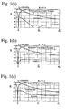
- Figs. 3(a) and (b) show the insertion loss, isolation and reflection loss of such a conventional two-port isolator by the solid line.
- a white triangle on the axis of ordinates indicates a reference line of 0 dB.
- this two-port isolator has a structure in which a thin garnet plate G having a diameter of 3.9 mm and a thickness of 0.4 mm is disposed in a 7-mm-square iron casing having a ferrite magnet fixed to an inner surface thereof, two perpendicularly crossing central conductors L 1 , L 2 are disposed in the vicinity of the ferrite magnet, and ceramic capacitors C 1 , C 2 are added.
- Fig. 3(a) shows the frequency characteristics of insertion loss and reflection loss of an input port (corresponding to the terminal (1) in Fig. 6), and Fig. 3(b) shows the frequency characteristics of isolation loss and reflection loss of an output port (corresponding to the terminal (2) in Fig. 6).
- the minimum value (0.58 dB) of insertion loss occurs at a frequency of 1140 MHz (center frequency f 0 ). This value is larger than the insertion loss of the three-port circulator by 0.2-0.3 dB.
- the isolation loss is about 11 dB at a center frequency f 0 , which is not necessarily so good.
- the frequency characteristics of the isolation loss of the two-port isolator are in an upward projecting curve, unlike a downward projecting curve in the three-port circulator.
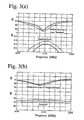
- Fig. 4 shows the insertion loss and isolation loss of the above two-port isolator measured in a wider frequency range than in Fig. 3.
- Fig. 4(a) shows the frequency characteristics of insertion loss and reflection loss of an input port
- Fig. 4(b) shows the frequency characteristics of isolation loss and reflection loss of an output port.
- Figs. 4(a) (b) show attenuation at 2 f 0 , 3 f 0 , wherein f 0 is a frequency of 1140 MHz at which the insertion loss is minimum.
- Fig. 4(b) also shows the insertion loss of Fig. 4(a) by a dotted line for comparison.
- this isolator reflects almost all at frequencies of 2 f 0 and 3 f 0 outside the bandwidth, with the attenuation of transmission of about 30 dB. What is better is that there is no unnecessary resonance as seen in the three-port circulator.
- the insertion loss and isolation loss have upward curved frequency characteristics.
- FIG. 8 shows the arrangement of central conductors L 1 , L 2 and a thin ferrite plate G in such a two-port isolator.
- Fig. 8(a) is a plan view showing the arrangement of a first thin ferrite plate piece G 1 and two central conductors L 1 , L 2 , with a second thin ferrite plate piece G 2 omitted.
- Fig. 8(b) is a cross-sectional view taken along the line A-A in Fig. 8(a).
- the second central conductor L 2 is perpendicularly disposed on the first central conductor L 1 via an insulating layer.
- the second thin ferrite plate piece G 2 is in close contact with the second central conductor L 2 .
- the arrow MF indicates a high-frequency magnetic field induced by a high-frequency electric current flowing through the central conductor L 1 .
- 3(a) and (b) indicate the insertion loss, isolation loss and reflection loss of a two-port isolator comprising a thin ferrite plate consisting only of a first thin ferrite plate piece G 1 without using a second thin ferrite plate piece G 2 .
- Fig. 16(a) shows a combination of central conductors L 1 , L 2 having two parallel conductor portions and a first, rectangular, thin ferrite plate G 1 in the conventional two-port isolator
- Fig. 16(b) shows a second thin ferrite plate piece G 2 disposed on the second central conductor L 2 in close contact.
- the coupling of the central conductors L 1 , L 2 is slightly larger in the assembly shown in Fig. 16 than in the assembly comprising a thin, circular ferrite plate as shown in Fig. 8.
- Fig. 17 The structure shown in Fig. 17 is the same as that shown in Fig. 16 except that two central conductors L 1 , L 2 are knitted. Because of this structure, the coupling of the two central conductors L 1 , L 2 can be improved.
- the conventional two-port isolator provides large isolation loss in a wide bandwidth, it is disadvantageous in having large insertion loss at a center frequency f o and a narrow bandwidth in which small insertion loss is obtained.
- an object of the present invention is to provide a two-port isolator having large isolation loss and small insertion loss in a wide bandwidth.
- Another object of the present invention is to provide a method for evaluating such a two-port isolator.
- the first two-port isolator of the present invention comprises a thin ferrite plate, a permanent magnet for applying a static magnetic field to the thin ferrite plate, first and second central conductors disposed substantially in a center portion of the thin ferrite plate and crossing each other with electric insulation, first and second input-output terminals each connected to an end of each of the first and second central conductors, a common terminal connected to the other ends of the first and second central conductors, a first matching capacitor connected between the first input-output terminal and the common terminal, a second matching capacitor connected between the second input-output terminal and the common terminal, and a resistor connected between the first input-output terminal and the second input-output terminal, wherein the DC resistance of the resistor is set, such that with loss in a high-frequency signal entering into the first input-output terminal and exiting from the second input-output terminal defined as insertion loss, and with loss in a high-frequency signal entering into the second input-output terminal and exiting from the first input-
- the isolation loss of the two-port isolator preferably increases by 1 dB or more, when a static magnetic field applied to the two-port isolator from outside increases by 800 A/m or more.
- a static magnetic field applied to the two-port isolator from outside is increased preferably by bringing a permanent magnet close to a casing serving as a magnetic yoke of the two-terminal isolator from above.
- the isolation loss of the two-port isolator preferably increases by 1 dB or more, when a permanent magnet having a residual magnetic flux density of 0.5 T or more is brought close to the casing within 50 mm from above.
- the resistor preferably has DC resistance of 60-100 ⁇ .
- the isolation is preferably 10 dB or more in a frequency range of 0.8 f 0 to 3 f 0 , wherein f 0 is a frequency at which the insertion loss is minimum.
- the method for evaluating a two-port isolator of the present invention which comprises a thin ferrite plate, a permanent magnet for applying a static magnetic field to the thin ferrite plate, first and second central conductors disposed substantially in a center portion of the thin ferrite plate and crossing each other with electric insulation, first and second input-output terminals each connected to an end of each of the first and second central conductors, a common terminal connected to the other ends of the first and second central conductors, a first matching capacitor connected between the first input-output terminal and the common terminal, a second matching capacitor connected between the second input-output terminal and the common terminal, and a resistor connected between the first input-output terminal and the second input-output terminal in a casing, comprises connecting the two-port isolator to an outside circuit; gradually bringing a permanent magnet close to the casing from outside to observe isolation loss while increasing a static magnetic field, wherein if the isolation increases by 1 dB or more when the static magnetic field increases by 800 A/m
- the second two-port isolator of the present invention comprises a thin ferrite plate, a permanent magnet for applying a static magnetic field to the thin ferrite plate, first and second central conductors disposed substantially in a center portion of the thin ferrite plate and crossing each other with electric insulation, first and second input-output terminals each connected to an end of each of the first and second central conductors, a common terminal connected to the other ends of the first and second central conductors, a first matching capacitor connected between the first input-output terminal and the common terminal, a second matching capacitor connected between the second input-output terminal and the common terminal, and a resistor connected between the first input-output terminal and the second input-output terminal, wherein the thin ferrite plate is constituted by one or more thin ferrite plate pieces, at least one thin ferrite plate piece being provided with a groove for receiving part of the central conductor.
- the thin ferrite plate is preferably formed by stacking at least two thin ferrite plate pieces, a first thin ferrite plate piece having a groove for receiving part of the central conductors, and a second thin ferrite plate piece being stacked thereon.
- the thin ferrite plate is preferably constituted by first and second thin ferrite plate pieces, the first thin ferrite plate piece having a first groove for receiving part of the first central conductor, and the second thin ferrite plate having a second groove for receiving part of the second central conductor.
- a plurality of thin ferrite plate pieces are preferably in contact with each other in regions other than the groove.
- a thin ferrite plate constituted by first and second thin ferrite plate pieces is preferably contained in a casing serving as a magnetic yoke having an inner surface, to which a permanent magnet is fixed; the first thin ferrite plate piece being disposed on the bottom side of the casing, while the second thin ferrite plate piece is disposed on the permanent magnet side; and the second thin ferrite plate piece having a larger saturation magnetization than that of the first thin ferrite plate piece.
- the difference in a saturation magnetization between the first thin ferrite plate piece and the second thin ferrite plate piece is preferably in a range of 0.005 T-0.02 T.
- the third two-port isolator of the present invention comprises a thin ferrite plate, a permanent magnet for applying a static magnetic field to the thin ferrite plate, first and second central conductors disposed substantially in a center portion of the thin ferrite plate and crossing each other with electric insulation, first and second input-output terminals each connected to an end of each of the first and second central conductors, a common terminal connected to the other ends of the first and second central conductors, a first matching capacitor connected between the first input-output terminal and the common terminal, a second matching capacitor connected between the second input-output terminal and the common terminal, and a resistor connected between the first input-output terminal and the second input-output terminal, wherein the thin ferrite plate is in a rectangular shape, and wherein the first and second central conductors each having three or more conductor portions are disposed on the rectangular, thin ferrite plate in parallel with its side.
- the first and second central conductors are preferably disposed between a plurality of thin ferrite plate pieces.
- the width of the central conductor is preferably 1/2 or more of a distance between the opposing . sides of the thin ferrite plate in parallel with the central conductor.
- the first and second central conductors are preferably disposed between the first and second thin ferrite plate pieces in close contact therewith, a static magnetic field being applied on the side of the second thin ferrite plate piece from the permanent magnet, and the second thin ferrite plate piece having a larger saturation magnetization than that of the first thin ferrite plate piece.
- the fourth two-port isolator of the present invention comprises a thin ferrite plate, a permanent magnet for applying a static magnetic field to the thin ferrite plate, first and second central conductors disposed substantially in a center portion of the thin ferrite plate and crossing each other with electric insulation, first and second input-output terminals each connected to an end of each of the first and second central conductors, a common terminal connected to the other ends of the first and second central conductors, a first matching capacitor connected between the first input-output terminal and the common terminal, a second matching capacitor connected between the second input-output terminal and the common terminal, and a resistor connected between the first input-output terminal and the second input-output terminal, wherein a crossing angle (on the resistor side) of the center axis of the first central conductor and the center axis of the second central conductor is in a range of 40-80°.
- a third capacitor is preferably connected in parallel with the resistor.
- the third capacitor preferably has smaller static capacitance than those of the first and second matching capacitors.
- An inductor is preferably connected in parallel with or in series to the resistor.
- the common terminal is preferably connected to a ground.
- Fig. 1 shows the frequency characteristics of the two-port isolator when the outside circuit impedance is 50 ⁇ .
- the outside circuit impedance is the impedance of an outside circuit to which the two-port isolator is connected, when viewed from the two-port isolator.
- Fig. 1(a) shows a case where the resistor R is 45 ⁇
- Fig. 1(b) shows a case where the resistor R is 50 ⁇
- Fig. 1(c) shows a case where the resistor R is 55 ⁇ .
- the center frequency f 0 is 1000 MHz
- the equivalent circuit is an ideal circuit
- insertion loss, isolation loss and the reflection loss of the input terminal in the two-port isolator were calculated by simulation.
- the frequency extends to the higher frequency side, particularly 2 f 0 and 3 f 0 .
- the isolation loss is infinite, the insertion loss is zero, and the reflection loss is infinite at a center frequency f 0 .
- the insertion loss tends to monotonously increase, without a particular singular point.
- the isolation loss is substantially flat on the higher frequency side, showing high attenuation of about 45 dB.
- the reflection loss of the input terminal is almost in a complete reflection state on the higher frequency side.
- the insertion loss and the reflection loss of the input terminal when the resistor R is 45 ⁇ are not largely different from those when the resistor R is 50 ⁇ .
- the isolation largely changes with attenuation of 25 dB at a center frequency f 0 .
- the isolation loss increases on the higher frequency side, showing an attenuation pole at a frequency of about 1.8 f 0 .
- the insertion loss and the reflection loss of the input terminal when the resistor R is 55 ⁇ are not largely different from those at 50 ⁇ .
- the isolation loss slowly and monotonously increases on the higher frequency side, without a singular point as shown in Fig. 1(a).
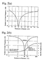
- Fig. 2(a) shows the calculation results of the isolation loss by simulation at a center frequency in a range of the resistor R of 20-110 Q.
- the isolation loss decreases regardless of whether the resistance of the resistor R is smaller or larger than the outside circuit impedance of 50 ⁇ .
- the resistor R should be in a range of 25-100 ⁇ .
- Fig. 2(b) shows the isolation loss determined at a center frequency in a wide resistance range of 1-1000 ⁇ , wider than the range of the resistance of the resistor R in Fig. 2(a).
- Fig. 2(b) shows a specific bandwidth of the reflection loss of the input terminal (percentage of a frequency width when the reflection loss reaches 20 dB to a center frequency f 0 ) in addition to the isolation loss.
- the isolation loss has a singular point when the resistance of the resistor R is 50 ⁇ , though the specific bandwidth tends to monotonously increase as the resistance of the resistor R increases. Namely, while the specific bandwidth is about 2% in a small R region, it is 10% in a large R region, close to an open state.
- the two-port isolator having the equivalent circuit shown in Fig. 6 loses irreversible characteristics as an isolator, when the resistance of the resistor R is too larger or smaller than 50 ⁇ . Namely, there is a desired range in the resistance of the resistor R.
- the crux of the present invention is to expand a bandwidth in which low insertion loss is obtained in the two-port isolator as much as possible, without decreasing the isolation loss. This has been achieved by expanding the bandwidth of the reflection loss of the input terminal as shown in Fig. 2(b). From this point of view, the optimum resistance of the resistor R was determined.
- the specific bandwidth of the reflection loss should be practically 4% or more. Accordingly, to expand the bandwidth of the reflection loss of the input terminal, it is clear from Fig. 2(b) that the resistance of the resistor R should be larger than the outside circuit impedance (50 Q). Also, to make the maximum of the isolation 10 dB or more, it is clear from Fig. 2(a) that the resistance of the resistor R should be 100 ⁇ or less.
- the outside circuit impedance of the isolator is just 50 ⁇ . Accordingly, the outside circuit impedance should be determined for each isolator. In a practical isolator, as shown in Figs. 3 and 4, even if the resistance of the resistor R were set at 50 ⁇ , the isolation loss would not become infinite. In the case of Figs. 3 and 4, the isolation loss is at most about 11 dB. This is because the outside circuit impedance of a portion to which the resistor R is connected is different from 50 ⁇ . Thus, it is important to know how high the outside circuit impedance of this portion is.
- the inventors have found that it is possible to determine which is larger between the outside circuit impedance and the resistor, by changing a magnetic field applied to a main surface of a thin ferrite plate while measuring the isolation loss of the two-port isolator by a network analyzer, etc.
- a static magnetic field applied to the thin ferrite plate can be changed, for instance, by bringing a permanent magnet near it from outside.
- the isolation loss increases. This means that the outside circuit impedance is higher than 50 ⁇ when no magnet nears. As shown in Fig. 1(b), because the isolation is the maximum when the outside circuit impedance is equal to the resistance of the resistor R, it is desirable that the resistance of the resistor R is higher than 50 ⁇ . Specifically, the isolation loss could be made 30 dB or more at a center frequency f 0 by setting the resistor R at about 70 ⁇ .
- the outside circuit impedance to which the isolator is tuned should be not 50 ⁇ but 70 ⁇ (see Fig. 2).
- the resistance of the resistor R is located on the left side (low resistance side) of the singular point of the isolation loss in Fig. 2(a). This is clear from the fact that the isolation loss has an attenuation peak near 2.5 f 0 in Fig. 4(b).
- the resistor R is not preferable to set the resistor R at 50 ⁇ in the two-port isolator of Figs. 3 and 4, and the resistor R is preferably located on the right side of the singular point of the isolation (higher resistance side) on Fig. 2(a) to obtain large isolation loss in a wide bandwidth. Namely, it is preferable to use a resistor having resistance larger than the resistance at which the isolation loss is the maximum. To determine whether or not the resistance of the resistor R of an actual two-port isolator is located on the right side of the singular point of the isolation loss on Fig.
- the isolation loss increases, namely, whether or not the isolation loss increases, when a static magnetic field applied to the thin ferrite plate is increased, for instance, by bringing permanent magnet near to the thin ferrite plate from outside.
- a static magnetic field applied to the thin ferrite plate is increased, for instance, by bringing permanent magnet near to the thin ferrite plate from outside.
- the isolation loss increases by at least 1 dB when a static magnetic field applied to the two-port isolator from outside is increased by 800 A/m or more, it can be confirmed that the resistor R has the desired resistance.
- the above is true when the two-port isolator shown in Fig. 6 is operated above resonance.
- the outside circuit impedance R is 70 ⁇ in the example of Figs. 3 and 4, the optimization of structure parameters could make the outside circuit impedance 50 ⁇ . Also, there is actually only extremely small demand to make the isolation loss more than 20 dB, and the isolation loss of less than 10 dB makes the function of the isolator meaningless in an actual use. Accordingly, when the outside circuit impedance is 50 ⁇ , it is determined from Fig. 2(a) that the desired lower limit of the resistance of the resistor R is 60 ⁇ , and that its desired upper limit is 100 ⁇ . Therefore, the desired range of the resistance of the resistor R is 60-100 ⁇ .
- the two-port isolator of the present invention can be provided with small input terminal reflection loss in a wide bandwidth by using a resistor R of 60-100 ⁇ . This makes it possible to provide the two-port isolator with small insertion loss in a wide bandwidth. Also, when controlled to have the above desired resistance, as shown in Fig. 1(c), the isolation loss can be made 10 dB or more in as wide a frequency range as 0.8 f 0 -3.0 f 0 .
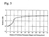
- a two-port isolator having a circuit shown in Fig. 6 was produced.
- a thin ferrite plate G was constituted by garnet-type ferrite having an outer diameter of 2.2 mm and a thickness of 0.4 mm, both matching capacitors C 1 , C 2 had capacitance of 2 pF, and a resistor R was 83 ⁇ .
- This two-port isolator had a center frequency of 2.0 GHz and isolation loss of 10.0 dB.
- a fully magnetized rare earth permanent magnet of 7 mm x 7 mm x 7 mm having a residual magnetic flux density of 1.1 T was brought near a casing of this two-terminal isolator from above, to increase a static magnetic field applied to the thin ferrite plate G.
- the relation between the isolation loss and the distance D between the permanent magnet and the casing is shown in Fig. 5.
- the isolation loss of the two-terminal isolator increased as the permanent magnet neared, and the isolation loss increased by 2 dB when the distance D became 2 mm.
- the resistor R can be regarded as having the desired resistance, if the isolation finally increases by 1 dB or more when a permanent magnet having a residual magnetic flux density of 0.5 T or more gradually nears from above to a point as close as 50 mm from the casing.
- the two-port isolator may be neared between the pole pieces of an electromagnet, instead of bringing a permanent magnet near the isolator from outside.
- the permanent magnet of the two-port isolator may be taken out, so that it is directly demagnetized or magnetized.
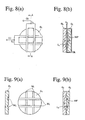
- Fig. 9 shows a thin ferrite plate according to one embodiment of the present invention.
- a thin ferrite plate piece G 1 is provided with grooves M 1 and M 2 for receiving the first and second central conductors L 1 , L 2 .
- Each groove M 1 , M 2 has two grooves to receive central conductors L 1 , L 2 each having parallel conductor portions. This makes it possible to efficiently couple a high-frequency magnetic field MF generated by the central conductors L 1 , L 2 to the thin ferrite plate G.
- the groove M 1 is slightly deeper than the groove M 2 .
- the coupling of the thin ferrite plate G and the central conductors L 1 , L 2 can be improved even with only one thin ferrite plate piece G 1 provided with grooves M 1 , M 2 shown in Fig. 9(a).
- the thin ferrite plate piece G 1 is preferably stacked with a thin ferrite plate piece G 2 without grooves to completely cover the central conductors L 1 , L 2 with the thin ferrite plate piece G 1 as shown in Fig. 9(b).
- the two thin ferrite plate pieces G 1 , G 2 are in close contact with each other in portions without grooves.
- Fig. 10 shows a thin ferrite plate piece according to another embodiment of the present invention.
- Fig. 10(a) shows a first thin ferrite plate piece G 1 provided with grooves M 1 , M 2 having width capable of receiving the overall central conductors L 1 , L 2
- Fig. 10(b) shows a second thin ferrite plate piece G 2 without grooves.
- Fig. 10(c) shows an assembly having two central conductors L 1 , L 2 between two thin ferrite plate pieces G 1 , G 2 .
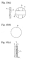
- Fig. 11 shows a thin ferrite plate and central conductors according to a still further embodiment of the present invention.
- Fig. 11 (a) shows a first thin ferrite plate piece G 1 provided with a first groove M 1 having a width capable of receiving the overall first central conductor L 1
- Fig. 11(b) shows a second thin ferrite plate piece G 2 provided with a second groove M 2 having a width capable of receiving the overall second central conductor L 2
- Fig. 11(c) shows an assembly having two central conductors L 1 , L 2 between the two thin ferrite plate pieces G 1 , G 2 .
- Fig. 12 shows a thin ferrite plate and central conductors according to a still further embodiment of the present invention.
- Fig. 12(a) shows a first thin ferrite plate piece G 1 provided with a first groove M 1 for receiving two conductor portions of the first central conductor L 1
- Fig. 12(b) shows a second thin ferrite plate piece G 2 provided with a second groove M 2 for receiving two conductor portions of the second central conductor L 2
- Fig. 12(c) shows an assembly having two central conductors L 1 , L 2 between the two thin ferrite plate pieces G 1 , G 2 .
- Fig. 13 shows a thin ferrite plate and central conductors according to a still further embodiment of the present invention.
- Fig. 13(a) shows a first thin ferrite plate piece G 1 having a groove M 1 such that two central conductors L 1 , L 2 can cross each other in two parallel conductor portions
- Fig. 13(b) shows a first thin ferrite plate piece G 1 having a projection only in a portion corresponding to the center portions of the central conductors L 1 , L 2
- a second thin ferrite plate piece G 2 (not shown) has a groove M 2 having the same shape as the groove M 1 , which perpendicularly crosses the groove M 1 of the first thin ferrite plate piece G 1 .
- Figs. 14(a) and (b) show a thin, rectangular ferrite plate and central conductors according to a still further embodiment of the present invention. This embodiment is the same as that shown in Fig. 12 except for the shape of the thin ferrite plate.
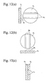
- Fig. 15 shows a magnetic circuit according to a still further embodiment of the present invention.
- Two thin ferrite plate pieces G 1 , G 2 are contained in a casing SH serving as a magnetic yoke having an inner surface, to which a permanent magnet MAG is fixed.
- the first thin ferrite plate piece G 1 is disposed on the lower side, and the second thin ferrite plate piece G 2 is disposed on the side of the permanent magnet MAG.
- a static magnetic field should be uniform in the thin ferrite plate. Because the magnetic circuit of Fig.
- the 15 has one permanent magnet MAG, a stronger magnetic field acts on the second thin ferrite plate piece G 2 near the permanent magnet MAG, and a relatively weak magnetic field acts on the first thin ferrite plate piece G 1 .
- it is desired to reduce the non-uniformity of the magnetic field. Effective as a method for reducing the non-uniformity of the magnetic field is to make the saturation magnetization of the second thin ferrite plate piece G 2 larger than that of the first thin ferrite plate piece G 1 .
- the insertion loss was determined by simulation, when thin ferrite plate pieces G 1 , G 2 both having a saturation magnetization of 0.09 T were used, and when the saturation magnetization of the thin ferrite plate piece G 2 was changed to four kinds, 0.095 T, 0.1 T, 0.11 T, and 0.12 T. As a result, it was found that when the thin ferrite plate piece G 2 had a saturation magnetization of 0.095 T, 0.1 T and 0.11 T, respectively, the insertion loss was small. When the saturation magnetization of the thin ferrite plate piece G 2 was as large as 0.12 T, the insertion loss rather increased.
- the difference in a saturation magnetization between the two thin ferrite plate pieces is preferably in a range of 0.005 T-0.02 T.
- Fig. 3(a) and (b) show the insertion loss, isolation loss and reflection loss of a two-port isolator comprising two thin ferrite plate pieces having grooves in Fig. 12.
- the minimum value of insertion loss decreased to about 0.40 dB at a frequency of 1140 MHz (center frequency f 0 ).
- This insertion loss is comparable to that of the three-port circulator.
- the isolation loss was about 14 dB at a center frequency f 0 , with slight improvement appreciated. Also, the bandwidth of the reflection loss of the input terminal was nearly doubled.
- Fig. 18 shows a combination of a thin ferrite plate and central conductors according to one embodiment of the present invention.
- a first central conductor L 1 having six parallel conductor portions is disposed on a first rectangular, thin ferrite plate piece G 1
- a second central conductor L 2 having six parallel conductor portions is substantially perpendicularly disposed on the first central conductor L 1 in close contact.
- Fig. 18(b) shows a second thin ferrite plate piece G 2 disposed on the second central conductor L 2 having six parallel conductor portions in close contact.
- the central conductors each having six parallel conductor portions are used in this embodiment, a high-frequency magnetic field generated by electric current flowing through the first central conductor is uniformly applied to the first and second thin ferrite plate pieces G 1 , G 2 entirely, whereby energy is transmitted to the second central conductor having six parallel conductor portions efficiently via the thin ferrite plate pieces G 1 , G 2 .
- This effect is obtained because the thin ferrite plate is rectangular. Because of improved coupling between the first and second central conductors L 1 , L 2 , the insertion loss is reduced in a wide bandwidth.
- W/S can be increased to 1/2 or more in the central conductor of the present invention having six parallel conductor portions, though W/S is 1/3-2/5 in the conventional central conductor having two parallel conductor portions.
- W/S is substantially 0.9.
- the simulation results indicate that W/S is preferably 1/2 or more.
- each central conductor preferably has three or more conductor portions.
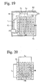
- Fig. 19 shows a rectangular casing SH containing a thin ferrite plate, two central conductors L 1 , L 2 , a resistor R, and matching capacitors C 1 , C 2 according to a still further embodiment of the present invention.
- a rectangular, thin ferrite plate piece G 1 is disposed in the rectangular casing SH slightly near one comer thereof. This provides space in diagonally opposing corners of the casing, where a resistor R and matching capacitors C 1 , C 2 are disposed.
- a long side of the rectangular, matching capacitor is close to each side of the thin ferrite plate in parallel.
- extremely efficient mounting can be achieved with high occupancy.
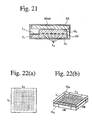
- Fig. 20 shows a combination of a thin ferrite plate and central conductors according to a still further embodiment of the present invention.
- conductor portions of the two central conductors L 1 , L 2 are knitted to provide strong coupling therebetween.
- Fig. 21 shows a cross section of the two-port isolator of Fig. 18, in which central conductors are incorporated.
- the first thin ferrite plate piece G 1 is disposed on the lower side of a casing SH, and the second thin ferrite plate piece G 2 is disposed on the side of a permanent magnet MAG.
- MAG permanent magnet
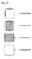
- Fig. 22 shows an assembly formed by attaching first and second central conductors to a plurality of ferrite sheets, laminating and sintering the ferrite sheets according to a still further embodiment of the present invention.
- Each central conductor is shown by a dotted line. Ends of the first and second central conductors L 1 , L 2 connected to input-output terminals are exposed on the upper surface of the thin ferrite plate as surface electrodes. Terminals GR of the first and second central conductors L 1 , L 2 connected to a ground are exposed on the lower surface of the thin ferrite plate.
- Fig. 23 is a development view of the thin ferrite plate of Fig. 22.
- a lowermost ferrite green sheet G 11 is relatively thick with a ground electrode GR printed on its rear surface.
- Laminated thereon is a relatively thin ferrite green sheet G 12 with the first central conductor L 1 printed on its surface.
- Laminated thereon is a relatively thin ferrite green sheet G 21 with the second central conductor L 2 printed on its surface in perpendicular to the first central conductor L 1 .
- An uppermost ferrite green sheet G 22 is relatively thick with external electrodes L 11 , L 21 to be connected to input-output terminals printed on its surface.
- Each ferrite green sheet G 11 , G 12 , G 21 , G 22 is composed of ferrite powder solidified with a binder. After pressing a laminate of four sheets, it is sintered at a high temperature to obtain a thin ferrite plate in which the first and second central conductors are embedded. Incidentally, with the sheet G 22 close to the permanent magnet set to have a large saturation magnetization, the static magnetic field can effectively be made uniform.
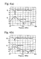
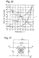
- Fig. 27 shows an equivalent circuit of the two-port isolator of the present invention. What is different from the two-port isolator shown in Fig. 6 is that the crossing angle ⁇ of the first and second central conductors is deviated from 90°, and that to compensate the effect of the crossing angle ⁇ , a third capacitor Cw is connected in parallel with the resistor R.
- Figs. 24(a), (b), (c) show the frequency characteristics of S parameters of a two-port isolator calculated by using the equivalent circuit of Fig. 27 in a frequency range of a center frequency f 0 of 1000 MHz ⁇ 10% (900 MHz-1100 MHz).
- Fig. 27 it is assumed that the two central conductors L 1 , L 2 are completely coupled.
- Used parameters are characteristic impedance Zo of 50 ⁇ , air-core inductance K of 1 nH, and a saturation magnetization 4 ⁇ Ms of the thin ferrite plate of 900 G, when the resistor R has a resistance of 50 ⁇ .
- Fig. 24 shows calculation results at three typical angles ⁇ of 60°, 90° and 120°.
- Cw to be minus means that it acts not as a capacitor but as an inductor.
- Fig. 24(a) shows the frequency characteristics of reflection loss S 11 .
- the reflection loss S 11 has a wide bandwidth when ⁇ is smaller than 90°, and the bandwidth rapidly narrows when ⁇ becomes larger than 90°.
- Fig. 24(b) also shows the frequency characteristics of insertion loss S 21 .
- the insertion loss S 21 at 900 MHz is indicated by a white triangle as IL (at 0.9f 0 ) because it is related to the bandwidth of insertion loss.
- Fig. 24(c) shows the frequency characteristics of isolation loss S 12 calculated under the same conditions.
- the isolation loss is deteriorated regardless of whether ⁇ becomes larger or smaller than 90°. Particularly when ⁇ is smaller than 90°, the deterioration of the isolation loss is remarkable.
- the isolation loss in a bandwidth of 0.96 f 0 (960 MHz) called IS (at 0.96f 0 ) is indicated by a white triangle. Large IS means that the bandwidth of isolation loss is wide.
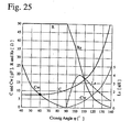
- Fig. 25 shows the variation of each parameter when the crossing angle ⁇ of the two central conductors changes in a wider range of 40°-140°.
- the first matching capacitor C 1 and the second matching capacitor C 2 have the same capacitance.
- Fig. 25 shows the changes of Ls and Rs at ⁇ > 90° in the right half thereof. As ⁇ becomes large, Rs rapidly approaches to zero, while Ls becomes maximum at 105°. When ⁇ is larger than it, Ls decreases monotonously.
- Fig. 26 shows the dependency of the characteristic parameters of isolator on angle calculated under the above conditions.
- the bandwidth of insertion loss S 21 indicated by IL (at 0.9 f 0 ) decreases as ⁇ becomes smaller than 90°, and becomes minimum at ⁇ of 60°, while it rapidly increases when ⁇ becomes larger than 90°.
- H res ( 2 ⁇ f 0 / ⁇ ) at a center frequency f 0 , expressed by a number with no dimension.
- ⁇ is a constant called a gyromagnetic ratio.
- the W (S 11 ) decreases monotonously.
- the lower limit of ⁇ is preferably 40°.
- the upper limit of ⁇ is preferably 80°.
- Cw should be considerably larger than C at a crossing angle ⁇ of 40° between the first and second central conductors, and Cw may be considerably small at ⁇ of 80°. In some cases, Cw may be unnecessary, because there is capacitance between both central conductors L 1 , L 2 due to the fact that two central conductors L 1 , L 2 crossing substantially in a center portion of the thin ferrite plate G are electrically insulated from each other with a thin insulating sheet, this capacitance functioning like Cw in Fig. 27 as an equivalent circuit. Therefore, with this inter-conductor capacitance properly set, the third capacitor Cw may be omitted. Also, with this inter-conductor capacitance, the third capacitor Cw may often practically be smaller than the first and second capacitors C.
- an inductor Lp may be connected in parallel with the resistor R to compensate this excess.
- the circuit of the resistor R and the inductor Lp may be replaced by the resistor Rs and the inductor Ls connected in series thereto.
- the resistance of the resistor connected between the first input-output terminal and the second input-output terminal set at the desired level larger than the outside circuit impedance, it is possible to obtain small insertion loss and large isolation in a wide bandwidth of a high-frequency signal. Also, by bringing a magnet near the isolator from outside, it is possible to evaluate whether or not the resistor of the two-terminal isolator has the desired resistance without difficulty.
- the coupling of the first central conductor and the second central conductor can be increased, thereby obtaining low insertion loss in a wide frequency bandwidth.
- the two-terminal isolator can be provided with small insertion loss in a wide bandwidth of a high-frequency signal.
- the two-terminal isolator can be provided with small insertion loss in a wide bandwidth of a high-frequency signal.
Landscapes
- Non-Reversible Transmitting Devices (AREA)
- Measurement Of Resistance Or Impedance (AREA)
Applications Claiming Priority (8)
| Application Number | Priority Date | Filing Date | Title |
|---|---|---|---|
| JP2001098589 | 2001-03-30 | ||
| JP2001098589 | 2001-03-30 | ||
| JP2001105382 | 2001-04-04 | ||
| JP2001105382A JP2002305404A (ja) | 2001-04-04 | 2001-04-04 | 2端子対アイソレータ |
| JP2001117461A JP2002314308A (ja) | 2001-04-16 | 2001-04-16 | 2端子対アイソレータ |
| JP2001117461 | 2001-04-16 | ||
| JP2001233692 | 2001-08-01 | ||
| JP2001233692A JP4655257B2 (ja) | 2001-08-01 | 2001-08-01 | 2端子対アイソレータ |
Publications (2)
| Publication Number | Publication Date |
|---|---|
| EP1246292A2 true EP1246292A2 (de) | 2002-10-02 |
| EP1246292A3 EP1246292A3 (de) | 2003-12-10 |
Family
ID=27482161
Family Applications (1)
| Application Number | Title | Priority Date | Filing Date |
|---|---|---|---|
| EP02007190A Withdrawn EP1246292A3 (de) | 2001-03-30 | 2002-03-28 | Zweiweg-Isolator und Verfahren zu seiner Beurteilung |
Country Status (4)
| Country | Link |
|---|---|
| US (1) | US6940360B2 (de) |
| EP (1) | EP1246292A3 (de) |
| KR (1) | KR100862962B1 (de) |
| CN (1) | CN1301567C (de) |
Cited By (1)
| Publication number | Priority date | Publication date | Assignee | Title |
|---|---|---|---|---|
| EP1615289A1 (de) | 2004-07-07 | 2006-01-11 | Hitachi Metals, Ltd. | Nichtreziproke Schaltungsanordnung |
Families Citing this family (8)
| Publication number | Priority date | Publication date | Assignee | Title |
|---|---|---|---|---|
| US6965276B2 (en) * | 2002-07-04 | 2005-11-15 | Murata Manufacturing Co., Ltd. | Two port type isolator and communication device |
| JP3663396B2 (ja) * | 2002-08-21 | 2005-06-22 | アルプス電気株式会社 | 非可逆回路素子 |
| JP3979402B2 (ja) * | 2003-09-04 | 2007-09-19 | 株式会社村田製作所 | 2ポート型アイソレータ、その特性調整方法および通信装置 |
| WO2006080172A1 (ja) * | 2005-01-28 | 2006-08-03 | Murata Manufacturing Co., Ltd. | 2ポート型非可逆回路素子及び通信装置 |
| CN101779328B (zh) * | 2007-08-22 | 2013-01-23 | 株式会社村田制作所 | 不可逆电路元件 |
| US7532084B2 (en) * | 2007-08-31 | 2009-05-12 | Murata Manufacturing Co., Ltd | Nonreciprocal circuit element |
| US8130054B1 (en) * | 2008-10-14 | 2012-03-06 | Rf Micro Devices, Inc. | Frequency-adjustable radio frequency isolator circuitry |
| CN111403884A (zh) * | 2020-03-27 | 2020-07-10 | 深圳市信维通信股份有限公司 | 贴片式环形器的制作方法 |
Citations (1)
| Publication number | Priority date | Publication date | Assignee | Title |
|---|---|---|---|---|
| US4016510A (en) * | 1976-05-03 | 1977-04-05 | Motorola, Inc. | Broadband two-port isolator |
Family Cites Families (6)
| Publication number | Priority date | Publication date | Assignee | Title |
|---|---|---|---|---|
| DE1050408B (de) * | 1956-11-09 | |||
| US3010085A (en) * | 1958-11-17 | 1961-11-21 | Bell Telephone Labor Inc | Isolators in lumped constant systems |
| US4101850A (en) | 1977-04-18 | 1978-07-18 | Motorola, Inc. | Uhf isolator using stacked conductor sheets |
| US4210886A (en) * | 1978-09-18 | 1980-07-01 | Motorola, Inc. | Isolator having reactive neutralizing means and predetermined angle between input-output windings |
| JP3264194B2 (ja) * | 1995-12-13 | 2002-03-11 | 株式会社村田製作所 | 非可逆回路素子 |
| JP3744168B2 (ja) * | 1998-01-19 | 2006-02-08 | 株式会社村田製作所 | アイソレータの製造方法 |
-
2002
- 2002-03-28 EP EP02007190A patent/EP1246292A3/de not_active Withdrawn
- 2002-03-29 US US10/108,360 patent/US6940360B2/en not_active Expired - Lifetime
- 2002-03-30 KR KR1020020017614A patent/KR100862962B1/ko not_active Expired - Lifetime
- 2002-03-30 CN CNB021272492A patent/CN1301567C/zh not_active Expired - Lifetime
Patent Citations (1)
| Publication number | Priority date | Publication date | Assignee | Title |
|---|---|---|---|---|
| US4016510A (en) * | 1976-05-03 | 1977-04-05 | Motorola, Inc. | Broadband two-port isolator |
Cited By (2)
| Publication number | Priority date | Publication date | Assignee | Title |
|---|---|---|---|---|
| EP1615289A1 (de) | 2004-07-07 | 2006-01-11 | Hitachi Metals, Ltd. | Nichtreziproke Schaltungsanordnung |
| US7382211B2 (en) | 2004-07-07 | 2008-06-03 | Hitachi Metals, Ltd. | Non-reciprocal circuit device |
Also Published As
| Publication number | Publication date |
|---|---|
| CN1389952A (zh) | 2003-01-08 |
| US20020171504A1 (en) | 2002-11-21 |
| EP1246292A3 (de) | 2003-12-10 |
| US6940360B2 (en) | 2005-09-06 |
| CN1301567C (zh) | 2007-02-21 |
| KR20020077277A (ko) | 2002-10-11 |
| KR100862962B1 (ko) | 2008-10-13 |
Similar Documents
| Publication | Publication Date | Title |
|---|---|---|
| US4236125A (en) | Wide band high power very high or ultra high frequency circulators | |
| US6215371B1 (en) | Non-reciprocal circuit element with a capacitor between the shield conductor and ground to lower the operating frequency | |
| US6940360B2 (en) | Two-port isolator and method for evaluating it | |
| EP0776060B1 (de) | Nichtreziprokes Schaltungselement | |
| KR100278345B1 (ko) | 비가역 회로소자 | |
| US7253697B2 (en) | Two-port isolator and communication apparatus | |
| Kagita et al. | Modeling of LTCC-Ferrite Tunable Inductors and Development of an $\boldsymbol {L} $-Band Phase Shifter | |
| CA1104668A (en) | Broadband isolator with stacked copper laminates | |
| US6642831B2 (en) | Nonreciprocal circuit device and communication device using same | |
| US6982608B2 (en) | Isolator suitable for miniaturization | |
| US7429901B2 (en) | Non-reciprocal circuit element, composite electronic component, and communication apparatus | |
| CN100468859C (zh) | 二端子对隔离器 | |
| US6844790B2 (en) | Non-reciprocal circuit device | |
| JPWO2006013865A1 (ja) | 非可逆回路素子 | |
| JP2003318608A (ja) | 非可逆回路素子 | |
| JP2007300605A (ja) | 非可逆回路素子 | |
| JP2002314308A (ja) | 2端子対アイソレータ | |
| JP2001358504A (ja) | 非可逆回路素子および通信装置 | |
| JP4315262B2 (ja) | 集中定数型非可逆回路素子 | |
| JP2002305404A (ja) | 2端子対アイソレータ | |
| CN105789739A (zh) | 一种微带线式铁氧体移相器 | |
| JP2001257507A (ja) | 非可逆回路素子および移動体通信端末 | |
| US6822527B2 (en) | Isolator for greatly attenuating signal transmitted in reverese direction over wide frequency band | |
| Okada et al. | An ultra miniature isolator with broadband isolation using ferrite gyrator | |
| JP2006246318A (ja) | 3巻線型非可逆素子 |
Legal Events
| Date | Code | Title | Description |
|---|---|---|---|
| PUAI | Public reference made under article 153(3) epc to a published international application that has entered the european phase |
Free format text: ORIGINAL CODE: 0009012 |
|
| AK | Designated contracting states |
Kind code of ref document: A2 Designated state(s): AT BE CH CY DE DK ES FI FR GB GR IE IT LI LU MC NL PT SE TR |
|
| AX | Request for extension of the european patent |
Free format text: AL;LT;LV;MK;RO;SI |
|
| PUAL | Search report despatched |
Free format text: ORIGINAL CODE: 0009013 |
|
| AK | Designated contracting states |
Kind code of ref document: A3 Designated state(s): AT BE CH CY DE DK ES FI FR GB GR IE IT LI LU MC NL PT SE TR |
|
| AX | Request for extension of the european patent |
Extension state: AL LT LV MK RO SI |
|
| 17P | Request for examination filed |
Effective date: 20040608 |
|
| AKX | Designation fees paid |
Designated state(s): DE FI FR GB IT |
|
| 17Q | First examination report despatched |
Effective date: 20090520 |
|
| STAA | Information on the status of an ep patent application or granted ep patent |
Free format text: STATUS: THE APPLICATION IS DEEMED TO BE WITHDRAWN |
|
| 18D | Application deemed to be withdrawn |
Effective date: 20091001 |