EP1237353A1 - Bildsensor mit schwarzen Pixeln, die räumlich verteilt zu den aktiven Bildpunkten angeordnet sind - Google Patents
Bildsensor mit schwarzen Pixeln, die räumlich verteilt zu den aktiven Bildpunkten angeordnet sind Download PDFInfo
- Publication number
- EP1237353A1 EP1237353A1 EP02075345A EP02075345A EP1237353A1 EP 1237353 A1 EP1237353 A1 EP 1237353A1 EP 02075345 A EP02075345 A EP 02075345A EP 02075345 A EP02075345 A EP 02075345A EP 1237353 A1 EP1237353 A1 EP 1237353A1
- Authority
- EP
- European Patent Office
- Prior art keywords
- image sensor
- black
- pixels
- black pixel
- pixel areas
- Prior art date
- Legal status (The legal status is an assumption and is not a legal conclusion. Google has not performed a legal analysis and makes no representation as to the accuracy of the status listed.)
- Withdrawn
Links
Images
Classifications
-
- H—ELECTRICITY
- H04—ELECTRIC COMMUNICATION TECHNIQUE
- H04N—PICTORIAL COMMUNICATION, e.g. TELEVISION
- H04N1/00—Scanning, transmission or reproduction of documents or the like, e.g. facsimile transmission; Details thereof
- H04N1/04—Scanning arrangements, i.e. arrangements for the displacement of active reading or reproducing elements relative to the original or reproducing medium, or vice versa
- H04N1/19—Scanning arrangements, i.e. arrangements for the displacement of active reading or reproducing elements relative to the original or reproducing medium, or vice versa using multi-element arrays
- H04N1/191—Scanning arrangements, i.e. arrangements for the displacement of active reading or reproducing elements relative to the original or reproducing medium, or vice versa using multi-element arrays the array comprising a one-dimensional [1D] array
- H04N1/192—Simultaneously or substantially simultaneously scanning picture elements on one main scanning line
- H04N1/193—Simultaneously or substantially simultaneously scanning picture elements on one main scanning line using electrically scanned linear arrays, e.g. linear CCD arrays
- H04N1/1934—Combination of arrays
-
- H—ELECTRICITY
- H04—ELECTRIC COMMUNICATION TECHNIQUE
- H04N—PICTORIAL COMMUNICATION, e.g. TELEVISION
- H04N25/00—Circuitry of solid-state image sensors [SSIS]; Control thereof
- H04N25/60—Noise processing, e.g. detecting, correcting, reducing or removing noise
- H04N25/63—Noise processing, e.g. detecting, correcting, reducing or removing noise applied to dark current
- H04N25/633—Noise processing, e.g. detecting, correcting, reducing or removing noise applied to dark current by using optical black pixels
-
- H—ELECTRICITY
- H10—SEMICONDUCTOR DEVICES; ELECTRIC SOLID-STATE DEVICES NOT OTHERWISE PROVIDED FOR
- H10F—INORGANIC SEMICONDUCTOR DEVICES SENSITIVE TO INFRARED RADIATION, LIGHT, ELECTROMAGNETIC RADIATION OF SHORTER WAVELENGTH OR CORPUSCULAR RADIATION
- H10F39/00—Integrated devices, or assemblies of multiple devices, comprising at least one element covered by group H10F30/00, e.g. radiation detectors comprising photodiode arrays
- H10F39/10—Integrated devices
- H10F39/12—Image sensors
- H10F39/18—Complementary metal-oxide-semiconductor [CMOS] image sensors; Photodiode array image sensors
-
- H—ELECTRICITY
- H10—SEMICONDUCTOR DEVICES; ELECTRIC SOLID-STATE DEVICES NOT OTHERWISE PROVIDED FOR
- H10F—INORGANIC SEMICONDUCTOR DEVICES SENSITIVE TO INFRARED RADIATION, LIGHT, ELECTROMAGNETIC RADIATION OF SHORTER WAVELENGTH OR CORPUSCULAR RADIATION
- H10F39/00—Integrated devices, or assemblies of multiple devices, comprising at least one element covered by group H10F30/00, e.g. radiation detectors comprising photodiode arrays
- H10F39/80—Constructional details of image sensors
- H10F39/802—Geometry or disposition of elements in pixels, e.g. address-lines or gate electrodes
-
- H—ELECTRICITY
- H10—SEMICONDUCTOR DEVICES; ELECTRIC SOLID-STATE DEVICES NOT OTHERWISE PROVIDED FOR
- H10F—INORGANIC SEMICONDUCTOR DEVICES SENSITIVE TO INFRARED RADIATION, LIGHT, ELECTROMAGNETIC RADIATION OF SHORTER WAVELENGTH OR CORPUSCULAR RADIATION
- H10F39/00—Integrated devices, or assemblies of multiple devices, comprising at least one element covered by group H10F30/00, e.g. radiation detectors comprising photodiode arrays
- H10F39/80—Constructional details of image sensors
- H10F39/803—Pixels having integrated switching, control, storage or amplification elements
-
- H—ELECTRICITY
- H10—SEMICONDUCTOR DEVICES; ELECTRIC SOLID-STATE DEVICES NOT OTHERWISE PROVIDED FOR
- H10F—INORGANIC SEMICONDUCTOR DEVICES SENSITIVE TO INFRARED RADIATION, LIGHT, ELECTROMAGNETIC RADIATION OF SHORTER WAVELENGTH OR CORPUSCULAR RADIATION
- H10F39/00—Integrated devices, or assemblies of multiple devices, comprising at least one element covered by group H10F30/00, e.g. radiation detectors comprising photodiode arrays
- H10F39/80—Constructional details of image sensors
- H10F39/805—Coatings
- H10F39/8057—Optical shielding
Definitions
- the present invention relates to image sensors and, more particularly, to such image sensors having black reference pixels located in a non-intrusive and more efficient position.
- black reference pixels located in the area immediately surrounding the active pixels. As is well known in the art, such black reference pixels are used for calibration of the imaging processing chain. These black reference pixels may become contaminated by lateral diffusion in which red light generated electrons from the active pixel area contaminate the first few rows and columns of the black reference pixels. This results in inaccurate reproduction of the desired image.
- CCD imaging sensors compensate for lateral diffusion by adding additional rows and columns of pixels in which these buffer pixel rows and columns absorb the lateral diffused energy.
- This solution requires the use of a secondary light shield that prevents illumination of the buffer pixel rows and columns.
- An alternate solution is to increase the number of black pixels beyond the amount normally needed. The extra black pixels are used to absorb the energy from lateral diffusion. In this case, a secondary light shield is not necessary.
- CMOS image sensors In CMOS image sensors, several layers of an inter-leaved material (usually metal) are used to shield light from the black reference pixels. These inter-leaved layers, however, allow light to leak therethrough and illuminate the black pixels, resulting in black pixels that are light sensitive. Obviously, this is an undesirable phenomenon.
- CMOS imagers the inter-leaved layers of material, used for black shielding, are not totally opaque to light.
- the solution to this problem is to add a secondary light shield, which in turn increases the cost.
- the present invention is directed to overcoming one or more of the problems set forth above.
- the invention resides in an image sensor comprising: (a) an active pixel area for image capture; (b) one or more black pixel areas disposed in a pre-determined, significant spaced apart distance from the active pixel area; and (c) a light shield to prevent light from illuminating the black pixel areas.
- the present invention has the advantage of improved performance black reference pixels in electronic imagers. This is accomplished through the use of a coverglass secondary light shield and geographically moving the black pixels a significant distance from the imaging pixels. This invention can be applied to all solid state imagers.
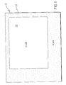
- the coverglass 10 includes a clear central portion 20 in which light is transmitted therethrough and a light-shielded outer portion 30 in which light is not transmitted therethrough.
- the secondary light-shield outer portion 30 is formed by opaque material such as epoxy, paints, glues; metal; or oxides. This opaque material serves two purposes. The first purpose is to attach the coverglass 10 to the imager package and the second purpose is to shield the black pixels from the incoming light. It is instructive to note that the coverglass 10 and glue are one assembly. It is possible to accomplish the same result by using a separate secondary light shield and coverglass as is well known in the art.
- the secondary light shield 30 may also be formed from an opaque material which is coated directly onto a surface of the image sensor.
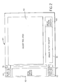
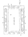
- the image sensor 40 includes an array of active picture pixels 50 arranged in a rectangular shape. As is well-known in the art, the active pixels 50 receive incident light which is converted into electrons and eventually a voltage for permitting capture of a digital representation of an image.
- Black reference pixels 60 are also shown a plurality of black reference pixels 60 and corresponding output multiplexing circuitry sections 70 both located at a predetermined significant distance from the active pixel area. The magnitude of the significant distance is established by the cone angle of the light of the focused image.
- the black pixels 60 are placed "far enough" under the secondary light shield such that image light can not illuminate the black pixels.
- Black reference pixels 60 are created by using active picture pixels with typically one or more metal layers deposited over them. The one or more metal layers are considered the primary light shield for the black pixels 60. Positioning the black reference pixels 60 at a significant distance from the active pixel area permits the opaque glue 30, on the coverglass 10, shown in Fig. 1, to shield light from the black pixels.
- the magnitude of the significant distance is determined by the optical design such that the black pixel signals aren't affected by either lateral diffusion or light sensitivity due to inter-leaved light shielding layers. This is accomplished by physically separating the black pixels 60 from the active image sensitive pixels 50 so no light illuminates the black pixels 60. Additional distance can be added such that the overall design is insensitive to inaccuracy of coverglass 10 positioning.
- black reference pixel sections 60 and corresponding output multiplexing circuitry sections may be used depending on the design.
- Multiple black reference pixel sections 60 provide additional black pixel information. For example, due to processing variation and temperature differences across the imager die, the dark reference signal can vary across the area of the imager. This is compensated for by the having multiple black reference pixel areas 60 located at various locations on the imager die. In summary, these multiple black reference pixel areas 60 allow more accurate measurement of the black signal for the total image. It is also instructive to note that additional black reference pixel areas 60 may be used, as the illustrated locations are for example only.
- the digital control circuitry 80, analog output circuitry 90 and analog to digital converter 100 are shown for reference purposes as is typical for the current state of the art. Such components are well known and will not be discussed in detail herein.
- the black reference pixel sections 60 are located at a plurality of positions. One location for the black reference pixel section 60 is between wire bond pads 110, and another location is on either side of the bond pads 110. These locations are in general located on any or all sides of the image area 50, separated a significant distance from the image area 50.
Landscapes
- Engineering & Computer Science (AREA)
- Multimedia (AREA)
- Signal Processing (AREA)
- Solid State Image Pick-Up Elements (AREA)
- Transforming Light Signals Into Electric Signals (AREA)
- Facsimile Heads (AREA)
Applications Claiming Priority (4)
| Application Number | Priority Date | Filing Date | Title |
|---|---|---|---|
| US26784901P | 2001-02-09 | 2001-02-09 | |
| US267849P | 2001-02-09 | ||
| US09/953,846 US6744526B2 (en) | 2001-02-09 | 2001-09-17 | Image sensor having black pixels disposed in a spaced-apart relationship from the active pixels |
| US953846 | 2001-09-17 |
Publications (1)
| Publication Number | Publication Date |
|---|---|
| EP1237353A1 true EP1237353A1 (de) | 2002-09-04 |
Family
ID=26952688
Family Applications (1)
| Application Number | Title | Priority Date | Filing Date |
|---|---|---|---|
| EP02075345A Withdrawn EP1237353A1 (de) | 2001-02-09 | 2002-01-28 | Bildsensor mit schwarzen Pixeln, die räumlich verteilt zu den aktiven Bildpunkten angeordnet sind |
Country Status (3)
| Country | Link |
|---|---|
| US (1) | US6744526B2 (de) |
| EP (1) | EP1237353A1 (de) |
| JP (1) | JP4053296B2 (de) |
Cited By (6)
| Publication number | Priority date | Publication date | Assignee | Title |
|---|---|---|---|---|
| US6744526B2 (en) * | 2001-02-09 | 2004-06-01 | Eastman Kodak Company | Image sensor having black pixels disposed in a spaced-apart relationship from the active pixels |
| WO2008027306A3 (en) * | 2006-08-31 | 2008-11-20 | Micron Technology Inc | Method, apparatus and system providing suppression of noise in a digital imager |
| GB2453544A (en) * | 2007-10-08 | 2009-04-15 | Keymed | Black level processing using independent black level sensor |
| US7969494B2 (en) | 2007-05-21 | 2011-06-28 | Aptina Imaging Corporation | Imager and system utilizing pixel with internal reset control and method of operating same |
| US8427542B2 (en) | 2009-04-20 | 2013-04-23 | Pixart Imaging Inc. | Image calibration method and image processing system utilizing the method |
| CN101883219B (zh) * | 2009-05-07 | 2014-02-19 | 原相科技股份有限公司 | 图像校正方法及使用此方法的图像处理系统 |
Families Citing this family (33)
| Publication number | Priority date | Publication date | Assignee | Title |
|---|---|---|---|---|
| US6786420B1 (en) | 1997-07-15 | 2004-09-07 | Silverbrook Research Pty. Ltd. | Data distribution mechanism in the form of ink dots on cards |
| US6618117B2 (en) | 1997-07-12 | 2003-09-09 | Silverbrook Research Pty Ltd | Image sensing apparatus including a microcontroller |
| US6985207B2 (en) | 1997-07-15 | 2006-01-10 | Silverbrook Research Pty Ltd | Photographic prints having magnetically recordable media |
| US6879341B1 (en) | 1997-07-15 | 2005-04-12 | Silverbrook Research Pty Ltd | Digital camera system containing a VLIW vector processor |
| AUPO802797A0 (en) | 1997-07-15 | 1997-08-07 | Silverbrook Research Pty Ltd | Image processing method and apparatus (ART54) |
| US7110024B1 (en) | 1997-07-15 | 2006-09-19 | Silverbrook Research Pty Ltd | Digital camera system having motion deblurring means |
| AUPO850597A0 (en) | 1997-08-11 | 1997-09-04 | Silverbrook Research Pty Ltd | Image processing method and apparatus (art01a) |
| US6690419B1 (en) | 1997-07-15 | 2004-02-10 | Silverbrook Research Pty Ltd | Utilising eye detection methods for image processing in a digital image camera |
| US20040119829A1 (en) | 1997-07-15 | 2004-06-24 | Silverbrook Research Pty Ltd | Printhead assembly for a print on demand digital camera system |
| US6624848B1 (en) | 1997-07-15 | 2003-09-23 | Silverbrook Research Pty Ltd | Cascading image modification using multiple digital cameras incorporating image processing |
| AUPP702098A0 (en) | 1998-11-09 | 1998-12-03 | Silverbrook Research Pty Ltd | Image creation method and apparatus (ART73) |
| AUPQ056099A0 (en) | 1999-05-25 | 1999-06-17 | Silverbrook Research Pty Ltd | A method and apparatus (pprint01) |
| US7084912B2 (en) * | 2001-09-20 | 2006-08-01 | Yuen-Shung Chieh | Method for reducing coherent row-wise and column-wise fixed pattern noise in CMOS image sensors |
| KR100448244B1 (ko) * | 2002-03-29 | 2004-09-13 | 주식회사 하이닉스반도체 | 이미지센서의 화소배열부 및 그를 포함하는 이미지센서 및이미지센서의 자동 블랙 레벨 보상 방법 |
| US7053458B2 (en) * | 2002-04-30 | 2006-05-30 | Ess Technology, Inc. | Suppressing radiation charges from reaching dark signal sensor |
| JP4246964B2 (ja) * | 2002-05-27 | 2009-04-02 | 浜松ホトニクス株式会社 | 固体撮像装置及び固体撮像装置アレイ |
| JP4018456B2 (ja) * | 2002-06-03 | 2007-12-05 | 富士フイルム株式会社 | 撮像装置 |
| US20050243193A1 (en) * | 2004-04-30 | 2005-11-03 | Bob Gove | Suppression of row-wise noise in an imager |
| JP4625685B2 (ja) * | 2004-11-26 | 2011-02-02 | 株式会社東芝 | 固体撮像装置 |
| KR100654342B1 (ko) * | 2005-02-07 | 2006-12-08 | 삼성전자주식회사 | 이미지 센서 |
| US7247829B2 (en) * | 2005-04-20 | 2007-07-24 | Fujifilm Corporation | Solid-state image sensor with an optical black area having pixels for detecting black level |
| KR100734272B1 (ko) * | 2005-08-30 | 2007-07-02 | 삼성전자주식회사 | 옵티컬 블랙 영역의 크기를 줄인 cmos 이미지 센서 |
| US20080239111A1 (en) * | 2007-03-26 | 2008-10-02 | Micron Technology, Inc. | Method and appratus for dark current compensation of imaging sensors |
| KR100881200B1 (ko) * | 2007-07-30 | 2009-02-05 | 삼성전자주식회사 | 씨모스 이미지 센서 및 그 제조방법 |
| JP5172362B2 (ja) * | 2008-01-10 | 2013-03-27 | シャープ株式会社 | 固体撮像装置および固体撮像装置の製造方法 |
| JP2010093753A (ja) * | 2008-10-10 | 2010-04-22 | Sony Corp | 固体撮像素子及び信号処理システム |
| DE102009004409A1 (de) * | 2009-01-13 | 2010-07-15 | Arnold & Richter Cine Technik Gmbh & Co. Betriebs Kg | Bildsensor |
| US8836835B2 (en) | 2010-10-04 | 2014-09-16 | International Business Machines Corporation | Pixel sensor cell with hold node for leakage cancellation and methods of manufacture and design structure |
| US8492214B2 (en) | 2011-03-18 | 2013-07-23 | International Business Machines Corporation | Damascene metal gate and shield structure, methods of manufacture and design structures |
| KR101442962B1 (ko) * | 2013-03-04 | 2014-09-23 | 주식회사 동부하이텍 | 이미지 센서 |
| US9526468B2 (en) | 2014-09-09 | 2016-12-27 | General Electric Company | Multiple frame acquisition for exposure control in X-ray medical imagers |
| US9560294B2 (en) | 2014-12-10 | 2017-01-31 | Semiconductor Components Industries, Llc | Systems and methods for pixel-level dark current compensation in image sensors |
| US9628730B2 (en) | 2015-01-27 | 2017-04-18 | Semiconductor Components Industries, Llc | Dark current gradient estimation using optically black pixels |
Citations (2)
| Publication number | Priority date | Publication date | Assignee | Title |
|---|---|---|---|---|
| EP0541332A1 (de) | 1991-11-04 | 1993-05-12 | Xerox Corporation | Architektur für analoge und digitale Bildsensoranordnungen |
| US5521639A (en) | 1992-04-30 | 1996-05-28 | Sony Corporation | Solid-state imaging apparatus including a reference pixel in the optically-black region |
Family Cites Families (2)
| Publication number | Priority date | Publication date | Assignee | Title |
|---|---|---|---|---|
| US6445413B1 (en) * | 1998-08-24 | 2002-09-03 | Xerox Corporation | System for determining a video offset from dark photosensors in an image sensor array |
| US6744526B2 (en) * | 2001-02-09 | 2004-06-01 | Eastman Kodak Company | Image sensor having black pixels disposed in a spaced-apart relationship from the active pixels |
-
2001
- 2001-09-17 US US09/953,846 patent/US6744526B2/en not_active Expired - Lifetime
-
2002
- 2002-01-25 JP JP2002017131A patent/JP4053296B2/ja not_active Expired - Lifetime
- 2002-01-28 EP EP02075345A patent/EP1237353A1/de not_active Withdrawn
Patent Citations (2)
| Publication number | Priority date | Publication date | Assignee | Title |
|---|---|---|---|---|
| EP0541332A1 (de) | 1991-11-04 | 1993-05-12 | Xerox Corporation | Architektur für analoge und digitale Bildsensoranordnungen |
| US5521639A (en) | 1992-04-30 | 1996-05-28 | Sony Corporation | Solid-state imaging apparatus including a reference pixel in the optically-black region |
Cited By (9)
| Publication number | Priority date | Publication date | Assignee | Title |
|---|---|---|---|---|
| US6744526B2 (en) * | 2001-02-09 | 2004-06-01 | Eastman Kodak Company | Image sensor having black pixels disposed in a spaced-apart relationship from the active pixels |
| WO2008027306A3 (en) * | 2006-08-31 | 2008-11-20 | Micron Technology Inc | Method, apparatus and system providing suppression of noise in a digital imager |
| US7969494B2 (en) | 2007-05-21 | 2011-06-28 | Aptina Imaging Corporation | Imager and system utilizing pixel with internal reset control and method of operating same |
| GB2453544A (en) * | 2007-10-08 | 2009-04-15 | Keymed | Black level processing using independent black level sensor |
| EP2048872A2 (de) | 2007-10-08 | 2009-04-15 | KeyMed (Medical & Industrial EqupmentT) Ltd | Vorrichtung und Verfahren zum Steuern des Schwarzanteils |
| GB2453544B (en) * | 2007-10-08 | 2012-02-29 | Keymed Medicals & Ind Equip | Black level control apparatus and method |
| US8384806B2 (en) | 2007-10-08 | 2013-02-26 | Keymed (Medical & Industrial Equipment) Ltd. | Black level control apparatus and method |
| US8427542B2 (en) | 2009-04-20 | 2013-04-23 | Pixart Imaging Inc. | Image calibration method and image processing system utilizing the method |
| CN101883219B (zh) * | 2009-05-07 | 2014-02-19 | 原相科技股份有限公司 | 图像校正方法及使用此方法的图像处理系统 |
Also Published As
| Publication number | Publication date |
|---|---|
| JP4053296B2 (ja) | 2008-02-27 |
| US6744526B2 (en) | 2004-06-01 |
| JP2002314758A (ja) | 2002-10-25 |
| US20020140997A1 (en) | 2002-10-03 |
Similar Documents
| Publication | Publication Date | Title |
|---|---|---|
| US6744526B2 (en) | Image sensor having black pixels disposed in a spaced-apart relationship from the active pixels | |
| US7508431B2 (en) | Solid state imaging device | |
| JP4786035B2 (ja) | 半導体装置 | |
| EP0559138B1 (de) | Festkörper-Bildaufnahmevorrichtung | |
| EP0893915A2 (de) | Kompakter Bildsensor mit daran befestigter Bildanzeigevorrichtung | |
| US5221848A (en) | High dynamic range film digitizer and method of operating the same | |
| US20220232184A1 (en) | Image sensing device | |
| US20120193549A1 (en) | Image pickup apparatus, radiation image pickup apparatus and radiation image pickup system | |
| US6753915B1 (en) | Photoelectric Conversion Apparatus and Image Pickup Apparatus having an Optimally Positioned Driving Wire | |
| KR930022571A (ko) | 전하 전송장치 및 고체 촬상장치 | |
| JPH07226495A (ja) | 減少されたフォトダイオード間のクロストークを有するccd画像センサー | |
| US5724094A (en) | Contact image sensor utilizing differential voltage pickoff | |
| US6127670A (en) | Solid-state color image sensor having an arrangement to compensate for dependence of light sensing characteristics upon color | |
| US6744032B1 (en) | Arrangement of microlenses in a solid-state image sensor for improving signal to noise ratio | |
| US20040173754A1 (en) | X-ray imager | |
| JPS61154283A (ja) | 固体撮像素子 | |
| GB2326525A (en) | Concentrators for light sensor arrays | |
| JPH0211193B2 (de) | ||
| JP4212447B2 (ja) | 固体撮像装置および電子カメラ | |
| JPS5736877A (en) | Solid state color photosensor | |
| JPH033269A (ja) | Ccd撮像素子 | |
| JPH03165568A (ja) | 固体撮像素子用パッケージ | |
| JPH11177073A (ja) | オンチップマイクロレンズ付固体撮像素子及びその製造方法 | |
| JP2546380B2 (ja) | 固体撮像素子 | |
| JP4370867B2 (ja) | 固体撮像装置 |
Legal Events
| Date | Code | Title | Description |
|---|---|---|---|
| PUAI | Public reference made under article 153(3) epc to a published international application that has entered the european phase |
Free format text: ORIGINAL CODE: 0009012 |
|
| AK | Designated contracting states |
Kind code of ref document: A1 Designated state(s): AT BE CH CY DE DK ES FI FR GB GR IE IT LI LU MC NL PT SE TR |
|
| AX | Request for extension of the european patent |
Free format text: AL;LT;LV;MK;RO;SI |
|
| 17P | Request for examination filed |
Effective date: 20021108 |
|
| 17Q | First examination report despatched |
Effective date: 20030331 |
|
| AKX | Designation fees paid |
Designated state(s): DE FR GB |
|
| RAP1 | Party data changed (applicant data changed or rights of an application transferred) |
Owner name: OMNIVISION TECHNOLOGIES, INC. |
|
| STAA | Information on the status of an ep patent application or granted ep patent |
Free format text: STATUS: THE APPLICATION IS DEEMED TO BE WITHDRAWN |
|
| 18D | Application deemed to be withdrawn |
Effective date: 20130801 |