EP1237239B1 - Circuit d'alimentation pour éléments à l'émission de lumière - Google Patents
Circuit d'alimentation pour éléments à l'émission de lumière Download PDFInfo
- Publication number
- EP1237239B1 EP1237239B1 EP02251424.4A EP02251424A EP1237239B1 EP 1237239 B1 EP1237239 B1 EP 1237239B1 EP 02251424 A EP02251424 A EP 02251424A EP 1237239 B1 EP1237239 B1 EP 1237239B1
- Authority
- EP
- European Patent Office
- Prior art keywords
- current
- light
- circuit
- emitting element
- frequency
- Prior art date
- Legal status (The legal status is an assumption and is not a legal conclusion. Google has not performed a legal analysis and makes no representation as to the accuracy of the status listed.)
- Expired - Lifetime
Links
- 238000001514 detection method Methods 0.000 claims description 8
- 230000003287 optical effect Effects 0.000 description 16
- 238000010586 diagram Methods 0.000 description 6
- 230000005669 field effect Effects 0.000 description 6
- 230000007423 decrease Effects 0.000 description 3
- 238000001816 cooling Methods 0.000 description 2
- 230000003292 diminished effect Effects 0.000 description 2
- 238000010438 heat treatment Methods 0.000 description 2
- 238000000034 method Methods 0.000 description 2
- 238000012986 modification Methods 0.000 description 2
- 230000004048 modification Effects 0.000 description 2
- 230000001360 synchronised effect Effects 0.000 description 2
- 230000009286 beneficial effect Effects 0.000 description 1
- 230000000295 complement effect Effects 0.000 description 1
- 230000003247 decreasing effect Effects 0.000 description 1
- 230000006866 deterioration Effects 0.000 description 1
- 238000012544 monitoring process Methods 0.000 description 1
- 230000010355 oscillation Effects 0.000 description 1
- 230000001172 regenerating effect Effects 0.000 description 1
- 230000000087 stabilizing effect Effects 0.000 description 1
Images


Classifications
-
- H—ELECTRICITY
- H01—ELECTRIC ELEMENTS
- H01S—DEVICES USING THE PROCESS OF LIGHT AMPLIFICATION BY STIMULATED EMISSION OF RADIATION [LASER] TO AMPLIFY OR GENERATE LIGHT; DEVICES USING STIMULATED EMISSION OF ELECTROMAGNETIC RADIATION IN WAVE RANGES OTHER THAN OPTICAL
- H01S5/00—Semiconductor lasers
- H01S5/04—Processes or apparatus for excitation, e.g. pumping, e.g. by electron beams
- H01S5/042—Electrical excitation ; Circuits therefor
- H01S5/0427—Electrical excitation ; Circuits therefor for applying modulation to the laser
Definitions
- the present invention relates to a light-emitting element drive circuit.
- An optical pickup is a device that is capable of reading information stored on the recording medium by monitoring the reflected light therefrom.
- a laser diode is also employed for writing information on to a recording medium. Drive circuits for such laser diodes have previously been developed.
- noise is also caused by instability of the light emission of the light-emitting element when light reflected by the storage medium returns to and enters the light-emitting element.
- High-frequency current is superimposed on the DC current component which is supplied to the light-emitting diode as the drive current.
- a suitable frequency for the high-frequency capable of being employed in current CD players is 300 to 500 MHz.
- the possibility of not supplying such high-frequency current to the light-emitting element has also been considered.
- the average value of the high-frequency current itself also varies with temperature and deterioration over a period of years.
- the level of the drive current varies.
- the decline of the light intensity increases the likelihood of occurrence of spurious detection being produced by small level variations. It is therefore preferable that level variation should be small.
- EP-A-0704948 describes a drive circuit pertaining to the features of the preamble of claim 1.
- JP-A-8288818 describes a drive circuit pertaining to the technological background of the invention.
- an object of the present invention is to provide a light-emitting element drive circuit in which drive current is produced by superimposing a high-frequency current component on a DC current component and supplying this to the light-emitting element but wherein level variation of this drive current can be suppressed.
- a light-emitting element drive circuit wherein, in first and second current mirror circuits having respective parallel lines, the respective one side of the lines is connected to the light-emitting element and respectively DC current and high-frequency current are passed to the respective other side of the lines in the first and second current mirror circuits, drive current resulting from the superposition of the high-frequency current on the DC current being supplied to the light-emitting element through the node of the connection, wherein the DC current component of the high-frequency current flowing through the second current mirror circuit is detected and the detected DC current component is arranged to be subtracted from the DC current flowing through the respective other side of the lines of the first current mirror circuit.
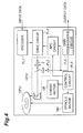
- Figure 4 is a circuit diagram of optical disk player using the circuit shown in figure 1 .
- a light-emitting element drive circuit according to an embodiment is described below. Identical elements are given the same reference symbols to avoid duplicated-description.
- This light-emitting element drive circuit comprises a main circuit wherein high-frequency current is superimposed on a DC current component and an auxiliary circuit for stabilizing the drive current. First of all, the main circuit will be described.
- Figure 1 is a circuit diagram of a main circuit in the light-emitting element drive circuit.
- Figures 3A, 3B, 3C, 3D, 3E, 3F, 3G, 3H, 3I and 3J are graphs illustrating current waveforms. The respective Figures indicating the waveforms of currents I1, I2, I3, I4, I5, I6, I7, I3', IL, IL' in the following description.
- This main circuit is a circuit wherein one each of lines (1A, 2A) in first and second current mirror circuits 1, 2 respectively having parallel lines (1A and 1B, 2A and 2B) is connected to a light-emitting element Z (the node is designated as X), while respectively DC current I1 and high-frequency current I4 (pulse current) are passed through the other ones (1B, 2B) of the aforesaid lines in these first and second current mirror circuits 1, 2.
- Current mirror circuits 1 and 2 respectively comprise two transistors (1QA and 1QB, 2QA and 2QB) and have two parallel lines (1A and 1B, 2A and 2B).
- the currents I3, I5 flowing through the lines on the one side 1A, 2A are respectively equal to or proportional to the currents I1, I4 flowing through the lines on the other side 1B, 2B.
- the pulse form drive current IL is the sum of the DC current I3 and the high-frequency current (pulse current) I5. However, these currents are equal to or proportional to the currents I1, I4 flowing in the lines 1B, 2B that are paired with the lines 1A, 2A through which these respectively flow, so the drive current IL is the sum or a value proportional to this sum of the DC current I1 and high-frequency current I4.
- the main circuit of this light-emitting element drive circuit supplies drive current IL obtained by superimposing high-frequency current I5 on DC current I3 through node X of the connection described above to light-emitting element Z.
- Transistor 1QB in this example is a p-channel field-effect transistor whose gate and drain are short-circuited.
- transistor 2QB is a p-channel field-effect transistor whose gate and drain are short-circuited, this high-frequency voltage will be applied thereto if the potential of the drain varies periodically. This drain potential is made to vary by a high-frequency generating circuit 3 connected with this drain.
- High-frequency generating circuit 3 is a current chopper circuit comprising n-channel field-effect transistors M5, M6; the drain of transistor M5 is connected with the drain of transistor 2QB. The total of the currents flowing through the two channels of these transistors M5, M6 is kept fixed by a constant current source 56.
- undesirable light reflected within the device enters the photodetector and becomes noise contained in the necessary information.
- Noise is also caused by instability of the light emission of the light-emitting element when light reflected by the storage medium returns to and enters the light-emitting element. Consequently, in order to suppress the noise, DC current is superimposed on the high-frequency current in the main circuit, and this is supplied to light-emitting element Z as drive current.
- a suitable frequency for the high-frequency capable of being employed in current CD players is 300 to 500 MHz.
- an auxiliary circuit is provided in the main circuit.
- FIG. 2 is a circuit diagram of a light-emitting element drive circuit wherein an auxiliary circuit is provided in addition to the main circuit.
- the auxiliary circuit comprises a detection circuit 4 that detects the DC current component I6' of the high-frequency current I4 (I5) flowing through second current mirror circuits 2 and an adjustment circuit 5 wherein the DC current component I6' detected by detection circuit 4 is subtracted from the DC current I1 (current I7 in Figure 2 ) flowing through the other side line 1B of the aforesaid lines of first current mirror circuit 1. This is described in detail below.
- Detection circuit 4 comprises a transistor M7 provided with a capacitative element (for AC removal) C interposed between the power source potential and ground.
- the gate of transistor M7 is connected with the gate of transistor 2QB in the second current mirror circuit 2, so that a voltage synchronized with and proportional to the high-frequency current I4 is applied between the gate of transistor M7 and the power source potential. That is, a high-frequency current I6 whose repetition frequency coincides with that of the high-frequency current I4 and whose amplitude is proportional thereto therefore flows between the source and drain of transistor M7.
- Transistor 2QB and transistor M7 constitute a current mirror circuit.
- Detection circuit 4 therefore indirectly detects the DC current component I6' of high-frequency current I4 (I5) flowing through the second current mirror circuit 2.
- Capacitative element C could be substituted by the gate capacitances of transistors 1QA and 1QB.
- Adjustment circuit 5 comprises a current superposition section Y in which DC current component I6' is superimposed on current I7 and a constant current source 45 that inputs the output current of current superposition section Y. That is, since a constant current I1 flows in constant current power source 45, when the detected DC current component I6' is increased, the current I7 flowing through the other-side line 1B of first current mirror 1 is decreased.
- (current I7) (current I1) - (current I6').
- adjustment circuit 5 subtracts the DC current-component I6' detected by detection circuit 4 from the DC current I7 flowing through the other side 1B of the aforesaid lines of first current mirror circuit 1.
- the drive current IL (IL') is the result of superimposition on the high-frequency current I5 of DC current I3' equal to or proportional to the DC current I7 flowing through the other-side line 1B of the first current mirror circuit 1, variation of the average value (level) of drive current IL' can be suppressed, by the amount of this increase (I6') being subtracted from drive current IL.
- transistors 1QA, 1QB, 2QA, 2QB and M7 were employed as transistors 1QA, 1QB, 2QA, 2QB and M7, their respective sources being connected with the power source potential, these could be substituted by for example PNP bipolar transistors.
- n-channel field-effect transistors were employed for transistors M5 and M6, their drains being connected with the power source potential, these could be substituted by for example NPN bipolar transistors.
- the source, gate and drain referred to in the case of the field-effect transistors should be regarded as emitter, base and collector in the case of bipolar transistors.
- the direction of current flow may be opposite to that described above.
- a suitable circuit with no external input may be provided between transistor 1QB and the node (current superposition section) Y.
- Figure 4 is a circuit diagram of optical disk player using the drive circuit shown in figure 1 .
- the input data for writing is encoded by an encoder PL1 such as EFM circuit.
- the encoded data is applied to for example a control terminal that controls the current flow of the current source 45.
- the light-emitting element Z, laser diode emits laser light in response to the encoded data.
- a recording layer of the optical disk OPD changes its physical structure and the data is recorded in the optical disk OPD.
- the reflected laser light beam by the optical disk OPD is detected by a photodiode PL3.
- the electric output from the photodiode PL3 is inputted into a data regenerative circuit PL4 and the recorded data is extracted.
- the electric output is also applied to an auto power control (APC) circuit PL5 that controls the power applied to the light-emitting element Z.
- the APC circuit PL5 is controlled by a control circuit PL6. Note that such an APC control is used during writing, too.
- the control circuit PL6 also controls a spindle motor SM for rotating the optical disk OPD and a linear motor LM for moving the optical pick-up unit OPU including light-emitting element Z.
- the electrical output from the photodiode PL3 may be used for focusing the laser light beam. This focusing technique is conventional.
- the control circuit PL6 decides the laser power by the required physical status of the recording layer when the optical disk is CD-RW. For example, a middle power heating by laser light beam and gradual cooling causes the recording layer to become a crystalline. High power heating and rapid cooling causes the recording layer to become amorphous.
- the control circuit PL6 may decide the laser power by the kind of the optical disk OPD because the required laser power differs by the kind of the optical disk.
- level variation of the drive current can be suppressed with the light-emitting element drive circuit of the present invention.
Landscapes
- Physics & Mathematics (AREA)
- Condensed Matter Physics & Semiconductors (AREA)
- General Physics & Mathematics (AREA)
- Electromagnetism (AREA)
- Optics & Photonics (AREA)
- Optical Head (AREA)
- Semiconductor Lasers (AREA)
- Electronic Switches (AREA)
Claims (1)
- Circuit d'attaque d'un élément électroluminescent comprenant :un premier circuit (1) à miroir de courant ayant des lignes parallèles (1A, 1B), l'une des lignes (1A, 1B) étant reliée à un élément électroluminescent (Z) via un noeud (X), et l'autre des lignes (1A, 1B) étant reliée à une source (45) de courant constant,un deuxième circuit (2) à miroir de courant ayant des lignes parallèles (2A, 2B), l'une des lignes (2A, 2B) étant reliée audit élément électroluminescent (2) via ledit noeud (X), et l'autre des lignes (2A, 2B) étant reliée à un circuit (3) de génération haute fréquence,caractérisé en ce que ledit circuit d'attaque d'un élément électroluminescent comprend en outre :un circuit de détection (4) pour détecter la composante de courant continu d'un courant haute fréquence circulant à travers ledit deuxième circuit (2) à miroir de courant ; etun moyen de soustraction pour soustraire la composante de courant continu détectée du courant continu circulant à travers l'autre des lignes (1A, 1B) dudit premier circuit (1) à miroir de courant.
Applications Claiming Priority (2)
| Application Number | Priority Date | Filing Date | Title |
|---|---|---|---|
| JP2001055284A JP4659235B2 (ja) | 2001-02-28 | 2001-02-28 | 発光素子駆動回路 |
| JP2001055284 | 2001-02-28 |
Publications (3)
| Publication Number | Publication Date |
|---|---|
| EP1237239A2 EP1237239A2 (fr) | 2002-09-04 |
| EP1237239A3 EP1237239A3 (fr) | 2004-12-01 |
| EP1237239B1 true EP1237239B1 (fr) | 2013-08-14 |
Family
ID=18915487
Family Applications (1)
| Application Number | Title | Priority Date | Filing Date |
|---|---|---|---|
| EP02251424.4A Expired - Lifetime EP1237239B1 (fr) | 2001-02-28 | 2002-02-28 | Circuit d'alimentation pour éléments à l'émission de lumière |
Country Status (3)
| Country | Link |
|---|---|
| US (1) | US6563274B2 (fr) |
| EP (1) | EP1237239B1 (fr) |
| JP (1) | JP4659235B2 (fr) |
Families Citing this family (6)
| Publication number | Priority date | Publication date | Assignee | Title |
|---|---|---|---|---|
| US6775529B1 (en) | 2000-07-31 | 2004-08-10 | Marvell International Ltd. | Active resistive summer for a transformer hybrid |
| US7606547B1 (en) | 2000-07-31 | 2009-10-20 | Marvell International Ltd. | Active resistance summer for a transformer hybrid |
| JP4444686B2 (ja) * | 2004-02-19 | 2010-03-31 | パナソニック株式会社 | レーザ光出射方法とその装置 |
| US7372882B2 (en) * | 2004-04-28 | 2008-05-13 | Renesas Technology Corp. | Driving circuit for and semiconductor device for driving laser diode |
| US7898185B2 (en) * | 2007-07-05 | 2011-03-01 | Mojarradi Mohammad M | Current controlled driver |
| DE602009000366D1 (de) * | 2008-04-25 | 2010-12-30 | Jds Uniphase Corp | Gleichstromgekoppelter Antrieb mit aktiver Terminierung |
Family Cites Families (16)
| Publication number | Priority date | Publication date | Assignee | Title |
|---|---|---|---|---|
| JPS59130494A (ja) * | 1983-08-08 | 1984-07-27 | Hitachi Ltd | 半導体レ−ザの駆動方法 |
| JPS60264130A (ja) * | 1984-06-12 | 1985-12-27 | Mitsubishi Electric Corp | レ−ザダイオ−ド駆動回路 |
| US4599494A (en) * | 1984-10-10 | 1986-07-08 | Motorola, Inc. | Ring sense telephone tone ringer circuit |
| GB2206010A (en) * | 1987-06-08 | 1988-12-21 | Philips Electronic Associated | Differential amplifier and current sensing circuit including such an amplifier |
| JP3061923B2 (ja) * | 1992-02-28 | 2000-07-10 | キヤノン株式会社 | 半導体発光素子の駆動回路 |
| JP3143887B2 (ja) * | 1992-07-24 | 2001-03-07 | ソニー株式会社 | レーザダイオード駆動回路および光ディスク装置 |
| JP2885120B2 (ja) * | 1995-01-27 | 1999-04-19 | 日本電気株式会社 | 演算増幅器 |
| JP3457763B2 (ja) * | 1995-04-13 | 2003-10-20 | アルプス電気株式会社 | 発光素子駆動回路 |
| JPH0974340A (ja) * | 1995-09-04 | 1997-03-18 | Toshiba Corp | コンパレータ回路 |
| JP2907140B2 (ja) * | 1996-08-23 | 1999-06-21 | 日本電気株式会社 | 変調歪測定装置 |
| JP3881079B2 (ja) * | 1997-03-14 | 2007-02-14 | 株式会社アドバンテスト | 半導体集積回路素子 |
| US5898334A (en) | 1997-05-12 | 1999-04-27 | Elantec Semiconductor, Inc. | Reduced output capacitance circuit for driving a grounded load in response to a stepped input |
| US6188059B1 (en) * | 1998-01-30 | 2001-02-13 | Sumitomo Electric Industries, Ltd. | Photocurrent monitor circuit and optical receiver |
| US6272160B1 (en) * | 1998-02-03 | 2001-08-07 | Applied Micro Circuits Corporation | High-speed CMOS driver for vertical-cavity surface-emitting lasers |
| JP4183310B2 (ja) * | 1998-10-08 | 2008-11-19 | 株式会社沖データ | 駆動回路ならびにこれを用いたプリンタおよびledヘッド |
| US6166530A (en) * | 2000-02-11 | 2000-12-26 | Advanced Analogic Technologies, Inc. | Current-Limited switch with fast transient response |
-
2001
- 2001-02-28 JP JP2001055284A patent/JP4659235B2/ja not_active Expired - Fee Related
-
2002
- 2002-02-28 EP EP02251424.4A patent/EP1237239B1/fr not_active Expired - Lifetime
- 2002-02-28 US US10/084,340 patent/US6563274B2/en not_active Expired - Fee Related
Also Published As
| Publication number | Publication date |
|---|---|
| JP4659235B2 (ja) | 2011-03-30 |
| US20020117974A1 (en) | 2002-08-29 |
| JP2002261382A (ja) | 2002-09-13 |
| EP1237239A2 (fr) | 2002-09-04 |
| EP1237239A3 (fr) | 2004-12-01 |
| US6563274B2 (en) | 2003-05-13 |
Similar Documents
| Publication | Publication Date | Title |
|---|---|---|
| EP0262713B1 (fr) | Méthode de commande par impulsions d'un laser à semi-conducteur, dispositif de commande pour un laser à semi-conducteur et appareil d'enregistrement à laser comprenant un tel dispositif de commande | |
| JP2605577B2 (ja) | 光ディスク記録装置 | |
| EP1237239B1 (fr) | Circuit d'alimentation pour éléments à l'émission de lumière | |
| KR100398752B1 (ko) | 레이저 구동회로 및 이를 이용한 기록장치 | |
| KR19980079877A (ko) | 반도체장치와 이를 포함하는 광픽업 광학계 유니트 및 이를 포함하는 광픽업장치 | |
| US20030099178A1 (en) | Optical disc drive and laser beam drive power supply voltage control method | |
| US7046612B2 (en) | Drive current supply circuit with current mirror | |
| JPS58158051A (ja) | 光学的記録再生装置 | |
| JPH0963093A (ja) | レーザ光出力制御回路 | |
| US7142485B2 (en) | Information storage apparatus | |
| JP5128655B2 (ja) | 電流駆動回路及びこれを含んだ光ストレージシステム | |
| JPH0737265A (ja) | 光情報記録装置 | |
| JP3440497B2 (ja) | レーザダイオード駆動回路 | |
| KR20070027936A (ko) | 레이저 다이오드 구동회로 및 그 제어방법과 레이저다이오드 구동용 반도체 집적회로 | |
| JP2000163782A (ja) | レーザ出力安定化装置 | |
| JP4083961B2 (ja) | 記録装置 | |
| JP3856804B2 (ja) | 光記録装置 | |
| KR870000697Y1 (ko) | 광 재생 장치의 포커스 서보회로 | |
| JP2007280464A (ja) | 光学的情報記録再生方法及び装置 | |
| JP2007272939A (ja) | 光ピックアップ | |
| JP2004172387A (ja) | 半導体レーザー駆動回路 | |
| WO2003088230A1 (fr) | Circuit de commande de laser a semi-conducteur et tete optique | |
| JPH09288839A (ja) | 光学式情報記録再生装置 | |
| JPH01296439A (ja) | 半導体レーザ制御回路 | |
| JPH08102078A (ja) | レーザ駆動回路 |
Legal Events
| Date | Code | Title | Description |
|---|---|---|---|
| PUAI | Public reference made under article 153(3) epc to a published international application that has entered the european phase |
Free format text: ORIGINAL CODE: 0009012 |
|
| AK | Designated contracting states |
Kind code of ref document: A2 Designated state(s): AT BE CH CY DE DK ES FI FR GB GR IE IT LI LU MC NL PT SE TR |
|
| AX | Request for extension of the european patent |
Free format text: AL;LT;LV;MK;RO;SI |
|
| PUAL | Search report despatched |
Free format text: ORIGINAL CODE: 0009013 |
|
| AK | Designated contracting states |
Kind code of ref document: A3 Designated state(s): AT BE CH CY DE DK ES FI FR GB GR IE IT LI LU MC NL PT SE TR |
|
| AX | Request for extension of the european patent |
Extension state: AL LT LV MK RO SI |
|
| 17P | Request for examination filed |
Effective date: 20050113 |
|
| 17Q | First examination report despatched |
Effective date: 20050518 |
|
| AKX | Designation fees paid |
Designated state(s): DE FR GB NL |
|
| RAP1 | Party data changed (applicant data changed or rights of an application transferred) |
Owner name: HAMAMATSU PHOTONICS K.K. |
|
| GRAP | Despatch of communication of intention to grant a patent |
Free format text: ORIGINAL CODE: EPIDOSNIGR1 |
|
| GRAS | Grant fee paid |
Free format text: ORIGINAL CODE: EPIDOSNIGR3 |
|
| GRAA | (expected) grant |
Free format text: ORIGINAL CODE: 0009210 |
|
| AK | Designated contracting states |
Kind code of ref document: B1 Designated state(s): DE FR GB NL |
|
| REG | Reference to a national code |
Ref country code: GB Ref legal event code: FG4D |
|
| REG | Reference to a national code |
Ref country code: NL Ref legal event code: T3 |
|
| REG | Reference to a national code |
Ref country code: DE Ref legal event code: R096 Ref document number: 60245369 Country of ref document: DE Effective date: 20131010 |
|
| PGFP | Annual fee paid to national office [announced via postgrant information from national office to epo] |
Ref country code: NL Payment date: 20140208 Year of fee payment: 13 |
|
| PGFP | Annual fee paid to national office [announced via postgrant information from national office to epo] |
Ref country code: FR Payment date: 20140211 Year of fee payment: 13 |
|
| PLBE | No opposition filed within time limit |
Free format text: ORIGINAL CODE: 0009261 |
|
| STAA | Information on the status of an ep patent application or granted ep patent |
Free format text: STATUS: NO OPPOSITION FILED WITHIN TIME LIMIT |
|
| PGFP | Annual fee paid to national office [announced via postgrant information from national office to epo] |
Ref country code: GB Payment date: 20140226 Year of fee payment: 13 |
|
| 26N | No opposition filed |
Effective date: 20140515 |
|
| REG | Reference to a national code |
Ref country code: DE Ref legal event code: R097 Ref document number: 60245369 Country of ref document: DE Effective date: 20140515 |
|
| PGFP | Annual fee paid to national office [announced via postgrant information from national office to epo] |
Ref country code: DE Payment date: 20140417 Year of fee payment: 13 |
|
| REG | Reference to a national code |
Ref country code: DE Ref legal event code: R119 Ref document number: 60245369 Country of ref document: DE |
|
| REG | Reference to a national code |
Ref country code: NL Ref legal event code: V1 Effective date: 20150901 |
|
| PG25 | Lapsed in a contracting state [announced via postgrant information from national office to epo] |
Ref country code: NL Free format text: LAPSE BECAUSE OF NON-PAYMENT OF DUE FEES Effective date: 20150901 |
|
| GBPC | Gb: european patent ceased through non-payment of renewal fee |
Effective date: 20150228 |
|
| REG | Reference to a national code |
Ref country code: FR Ref legal event code: ST Effective date: 20151030 |
|
| PG25 | Lapsed in a contracting state [announced via postgrant information from national office to epo] |
Ref country code: DE Free format text: LAPSE BECAUSE OF NON-PAYMENT OF DUE FEES Effective date: 20150901 Ref country code: GB Free format text: LAPSE BECAUSE OF NON-PAYMENT OF DUE FEES Effective date: 20150228 |
|
| PG25 | Lapsed in a contracting state [announced via postgrant information from national office to epo] |
Ref country code: FR Free format text: LAPSE BECAUSE OF NON-PAYMENT OF DUE FEES Effective date: 20150302 |