EP1235264A2 - Direkte Ätzung von dünnschichter Wiederstand mittels einer harten Maske - Google Patents
Direkte Ätzung von dünnschichter Wiederstand mittels einer harten Maske Download PDFInfo
- Publication number
- EP1235264A2 EP1235264A2 EP02010084A EP02010084A EP1235264A2 EP 1235264 A2 EP1235264 A2 EP 1235264A2 EP 02010084 A EP02010084 A EP 02010084A EP 02010084 A EP02010084 A EP 02010084A EP 1235264 A2 EP1235264 A2 EP 1235264A2
- Authority
- EP
- European Patent Office
- Prior art keywords
- hard mask
- thin film
- film resistor
- tiw
- resistor
- Prior art date
- Legal status (The legal status is an assumption and is not a legal conclusion. Google has not performed a legal analysis and makes no representation as to the accuracy of the status listed.)
- Withdrawn
Links
Images

Classifications
-
- H—ELECTRICITY
- H10—SEMICONDUCTOR DEVICES; ELECTRIC SOLID-STATE DEVICES NOT OTHERWISE PROVIDED FOR
- H10P—GENERIC PROCESSES OR APPARATUS FOR THE MANUFACTURE OR TREATMENT OF DEVICES COVERED BY CLASS H10
- H10P76/00—Manufacture or treatment of masks on semiconductor bodies, e.g. by lithography or photolithography
- H10P76/40—Manufacture or treatment of masks on semiconductor bodies, e.g. by lithography or photolithography of masks comprising inorganic materials
- H10P76/405—Manufacture or treatment of masks on semiconductor bodies, e.g. by lithography or photolithography of masks comprising inorganic materials characterised by their composition, e.g. multilayer masks
-
- H—ELECTRICITY
- H10—SEMICONDUCTOR DEVICES; ELECTRIC SOLID-STATE DEVICES NOT OTHERWISE PROVIDED FOR
- H10D—INORGANIC ELECTRIC SEMICONDUCTOR DEVICES
- H10D1/00—Resistors, capacitors or inductors
- H10D1/40—Resistors
- H10D1/47—Resistors having no potential barriers
- H10D1/474—Resistors having no potential barriers comprising refractory metals, transition metals, noble metals, metal compounds or metal alloys, e.g. silicides
-
- H—ELECTRICITY
- H10—SEMICONDUCTOR DEVICES; ELECTRIC SOLID-STATE DEVICES NOT OTHERWISE PROVIDED FOR
- H10P—GENERIC PROCESSES OR APPARATUS FOR THE MANUFACTURE OR TREATMENT OF DEVICES COVERED BY CLASS H10
- H10P50/00—Etching of wafers, substrates or parts of devices
- H10P50/60—Wet etching
- H10P50/66—Wet etching of conductive or resistive materials
- H10P50/663—Wet etching of conductive or resistive materials by chemical means only
- H10P50/667—Wet etching of conductive or resistive materials by chemical means only by liquid etching only
-
- H—ELECTRICITY
- H10—SEMICONDUCTOR DEVICES; ELECTRIC SOLID-STATE DEVICES NOT OTHERWISE PROVIDED FOR
- H10P—GENERIC PROCESSES OR APPARATUS FOR THE MANUFACTURE OR TREATMENT OF DEVICES COVERED BY CLASS H10
- H10P50/00—Etching of wafers, substrates or parts of devices
- H10P50/71—Etching of wafers, substrates or parts of devices using masks for conductive or resistive materials
-
- H—ELECTRICITY
- H10—SEMICONDUCTOR DEVICES; ELECTRIC SOLID-STATE DEVICES NOT OTHERWISE PROVIDED FOR
- H10P—GENERIC PROCESSES OR APPARATUS FOR THE MANUFACTURE OR TREATMENT OF DEVICES COVERED BY CLASS H10
- H10P76/00—Manufacture or treatment of masks on semiconductor bodies, e.g. by lithography or photolithography
- H10P76/40—Manufacture or treatment of masks on semiconductor bodies, e.g. by lithography or photolithography of masks comprising inorganic materials
- H10P76/408—Manufacture or treatment of masks on semiconductor bodies, e.g. by lithography or photolithography of masks comprising inorganic materials characterised by their sizes, orientations, dispositions, behaviours or shapes
- H10P76/4085—Manufacture or treatment of masks on semiconductor bodies, e.g. by lithography or photolithography of masks comprising inorganic materials characterised by their sizes, orientations, dispositions, behaviours or shapes characterised by the processes involved to create the masks
-
- Y—GENERAL TAGGING OF NEW TECHNOLOGICAL DEVELOPMENTS; GENERAL TAGGING OF CROSS-SECTIONAL TECHNOLOGIES SPANNING OVER SEVERAL SECTIONS OF THE IPC; TECHNICAL SUBJECTS COVERED BY FORMER USPC CROSS-REFERENCE ART COLLECTIONS [XRACs] AND DIGESTS
- Y10—TECHNICAL SUBJECTS COVERED BY FORMER USPC
- Y10S—TECHNICAL SUBJECTS COVERED BY FORMER USPC CROSS-REFERENCE ART COLLECTIONS [XRACs] AND DIGESTS
- Y10S148/00—Metal treatment
- Y10S148/136—Resistors
Definitions
- the present invention relates to methods of etching thin film resistor material, by cleanly etching CrSi to form thin film resistors in semiconductor devices.
- Thin film resistors are well known and may comprise a variety of resistive materials, with the chromium-based resistive materials chromium silicide (CrSi) being common.
- Thin film resistors may include an electrical interconnect contacting the resistive material for passing a current therethrough. The efficiency and accuracy of the thin film resistor depends upon the condition of the resistive material and the cleanliness of the portion of the resistor contacting the electrical interconnect. Resistive material that is corroded or contaminated ( e . g . has highly oxidized chromium) is undesirable because such conditions adversely affect the sheet resistance of the resistor. A "dirty" contact between the resistive material and the electrical interconnect adversely affects the contact resistance of the resistor.
- US-A-4035208 describes for a method of patterning platinum over a copper lager without affecting the copper layer the deposition of a tantalum mask in the same pump-down to that used with the deposition of chromeplatinum.
- the tantalum layer is then patterned using a photolithographic masking and a F4 plasma-vapor etch, whereby the chromium layer is left intact due to the plasma-vapor etch.
- US-A-3634159 describes an electrical circuit assembly using plated gold conductors on a substrate having a resistive coating made of nickl chromium (NiCr) to provide resistors in areas where the gold layer is not removed with an etchant.
- US-A-5043295 describes thin film resistors made of silicon chronium (SiCr) which are etched through a delineated titanium-tungsten hard mask (TiW). For etching TiW hydrogen peroxide (H 2 O 2 ) is used.
- US-A-5374569 describes thin film resistors made of SiCr which are delineated with a TiW hard mask without indicating the etching material used.
- US-A-4081315 describes resistors of Cermet which are delineated by use of phosphoric acid (P 2 O 5 ) through a molybdenum (Mo) hard mask.
- US-A-3649945 describes thin film resistors such as NiCr which are delineated by use of Mo.
- the Mo layer is also used as intermediate layer for the aluminium interconnet layer. Due to the desclosure of this prior patent specification titanium and tungsten are difficult or impossible to etch with an etchant that does not also attack the resistive film.
- the present provides a method of making at least one thin film resistor in a semiconductor device as claimed in claim 1.
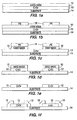
- a thin film resistor material 12 such as CrSi
- a hard mask 10 may be deposited over the resistor material 12 without breaking vacuum over the resistor material 12.
- the hard mask 10 may be deposited on the resistor material 12 in a deposition chamber without breaking the vacuum within the deposition chamber so that no contaminating materials are between the hard mask 10 and the material 12.
- the hard mask 10 is a non-photoresist material that is not affected by the etching effects of an etchant that may be used to etch the resistor material 12, namely a mixture of phosphoric acid, nitric acid and hydrofluoric acid for a CrSi thin film resistor.
- the hard mask 10 is comprised of TiW.
- Figure 1b shows the hard mask 10 delineated by depositing a PR mask 16 on the hard mask 10 and patterning the PR mask 16 so that it remains on the portions of the hard mask 10 overlying the portions of the resistor material 12 that will become the thin film resistors. Thereafter, as shown in Figure 1c, the hard mask 10 is etched with a first etchant to expose the portions of the resistor material 12 that will be etched.
- the first etchant may be any known etchant that does not contaminate or otherwise adversely affect the PR mask 16 and the resistor material 12.
- the first etchant is comprised of hydrogen peroxide.
- Figure 1d shows the PR mask 16 which may then be removed by using, for example, a solvent strip, and thereafter, the resistor material 12 may be etched with a second etchant to remove unwanted thin film resistor material.
- the second etchant may be any known etchant that cleanly and uniformly etches the resistor material 12, that does not leave behind residue or contaminants which adversely affect the resistor material 12, or that does not otherwise adversely affect the resistor material 12.
- the second etchant may be such that it does not have an etching effect on the hard mask 10.
- the second etchant for CrSi is comprised of a mixture of phosphoric acid, nitric acid and hydrofluoric acid.
- An acceptable mixture of the latter second etchant is the known etchant comprised of 97% phosphoric acid, 2% nitric acid and 1% hydrofluoric acid.
- the remaining hard mask portions may be removed with an etchant that does not adversely affect the resistor material 12, such as hydrogen peroxide, thereby leaving behind clean resistor material 12 for contacting electrical interconnects.
- electrical interconnects 18 may be deposited and delineated on the resistor material 12 thereby forming plural resistors on a semiconductor substrate 14.
- the electrical interconnects 18 may be comprised of any electrically conductive material, with aluminum being preferred.
- the thin film resistors thereby formed are free of contamination that may affect contact resistance with the interconnect.
- a photoresist may be used to delineate the interconnects 18.
- the electrical interconnect deposition and delineation may be performed prior to the removal of the delineated hard mask 10 from the resistor material 12 as shown in Figure 2a so that the PR, PR solvent strip and interconnect metalization do not contact and contaminate the surface of the resistor material 12. More specifically, the electrical interconnect 18 is deposited and patterned with a PR mask, the unwanted portions of the electrical interconnect are etched with a suitable etchant, and the remaining PR is then removed with, for example, a solvent strip.
- the portions of the hard mask not underlying the electrical interconnects are etched with an etchant that does not adversely affect the electrical interconnects 18 thereby leaving hard mask portions 20 between the electrical interconnects 18 and the resistor material 12.
- the hard mask is etched with hydrogen peroxide.
- the portions of the hard mask 20 between the resistor material 12 and the electrical interconnects 18 act as barriers and prevent interdiffusion between the resistor material 12 and the electrical interconnects 18 without significant effect on the electrical connection.
- the thin film resistors thereby formed are free of PR contamination and interconnect metalization across their surface.
- portions of the hard mask may be etched leaving behind those portions of the hard mask 22 overlying the portions of the resistor material 12 that are for contacting electrical interconnects.
- the electrical interconnects 18 may be deposited over portions of the remaining hard mask 22 thereby leaving hard mask portions 22 between the electrical interconnect 18 and the resistor material 12.
- the portions of the hard mask 22 between the resistor material 12 and the electrical interconnects 18 act as barriers and prevent interdiffusion between the resistor material 12 and the electrical interconnects 18 without significant effect on the electrical connection.
- the second etchant may be a mixture of phosphoric acid, nitric acid and hydrofluoric acid for CrSi.
- the hard mask preferably comprises TiW.
Landscapes
- Semiconductor Integrated Circuits (AREA)
- Internal Circuitry In Semiconductor Integrated Circuit Devices (AREA)
- ing And Chemical Polishing (AREA)
- Weting (AREA)
- Manufacturing Of Printed Circuit Boards (AREA)
Priority Applications (1)
| Application Number | Priority Date | Filing Date | Title |
|---|---|---|---|
| EP02777144A EP1466264B1 (de) | 1995-12-29 | 2002-09-18 | Verfahren zur konfiguration der verbindung zwischen datenverarbeitungszellen |
Applications Claiming Priority (3)
| Application Number | Priority Date | Filing Date | Title |
|---|---|---|---|
| US08/387,233 US5547896A (en) | 1995-02-13 | 1995-02-13 | Direct etch for thin film resistor using a hard mask |
| US387233 | 1995-02-13 | ||
| EP95120743A EP0726597B1 (de) | 1995-02-13 | 1995-12-29 | Direkte Ätzung von einem Dünnschicht-Widerstand mittels einer harten Maske |
Related Parent Applications (1)
| Application Number | Title | Priority Date | Filing Date |
|---|---|---|---|
| EP95120743A Division EP0726597B1 (de) | 1995-02-13 | 1995-12-29 | Direkte Ätzung von einem Dünnschicht-Widerstand mittels einer harten Maske |
Publications (2)
| Publication Number | Publication Date |
|---|---|
| EP1235264A2 true EP1235264A2 (de) | 2002-08-28 |
| EP1235264A3 EP1235264A3 (de) | 2002-10-02 |
Family
ID=23529041
Family Applications (2)
| Application Number | Title | Priority Date | Filing Date |
|---|---|---|---|
| EP95120743A Expired - Lifetime EP0726597B1 (de) | 1995-02-13 | 1995-12-29 | Direkte Ätzung von einem Dünnschicht-Widerstand mittels einer harten Maske |
| EP02010084A Withdrawn EP1235264A3 (de) | 1995-02-13 | 1995-12-29 | Direkte Ätzung von dünnschicht Wiederstand mittels einer harten Maske |
Family Applications Before (1)
| Application Number | Title | Priority Date | Filing Date |
|---|---|---|---|
| EP95120743A Expired - Lifetime EP0726597B1 (de) | 1995-02-13 | 1995-12-29 | Direkte Ätzung von einem Dünnschicht-Widerstand mittels einer harten Maske |
Country Status (5)
| Country | Link |
|---|---|
| US (1) | US5547896A (de) |
| EP (2) | EP0726597B1 (de) |
| JP (1) | JPH08241883A (de) |
| KR (1) | KR960032101A (de) |
| DE (1) | DE69530668D1 (de) |
Cited By (1)
| Publication number | Priority date | Publication date | Assignee | Title |
|---|---|---|---|---|
| CN113410382A (zh) * | 2021-06-15 | 2021-09-17 | 西安微电子技术研究所 | 一种铬硅系薄膜电阻及其制备方法 |
Families Citing this family (37)
| Publication number | Priority date | Publication date | Assignee | Title |
|---|---|---|---|---|
| US5683928A (en) * | 1994-12-05 | 1997-11-04 | General Electric Company | Method for fabricating a thin film resistor |
| US5675310A (en) * | 1994-12-05 | 1997-10-07 | General Electric Company | Thin film resistors on organic surfaces |
| JP3079027B2 (ja) * | 1995-11-28 | 2000-08-21 | インターナショナル・ビジネス・マシーンズ・コーポレ−ション | ウエットエッチング方法、ウエットエッチング装置 |
| US6262434B1 (en) * | 1996-08-23 | 2001-07-17 | California Micro Devices Corporation | Integrated circuit structures and methods to facilitate accurate measurement of the IC devices |
| CA2193905A1 (en) * | 1996-12-24 | 1998-06-24 | Luc Ouellet | Integrated processing for an etch module |
| US5976944A (en) * | 1997-02-12 | 1999-11-02 | Harris Corporation | Integrated circuit with thin film resistors and a method for co-patterning thin film resistors with different compositions |
| US6040226A (en) * | 1997-05-27 | 2000-03-21 | General Electric Company | Method for fabricating a thin film inductor |
| US6143649A (en) * | 1998-02-05 | 2000-11-07 | Micron Technology, Inc. | Method for making semiconductor devices having gradual slope contacts |
| US6441447B1 (en) * | 1998-02-12 | 2002-08-27 | Intersil Corporation | Co-patterning thin-film resistors of different compositions with a conductive hard mask and method for same |
| US6087269A (en) * | 1998-04-20 | 2000-07-11 | Advanced Micro Devices, Inc. | Method of making an interconnect using a tungsten hard mask |
| US6921962B1 (en) | 1998-12-18 | 2005-07-26 | Texas Instruments Incorporated | Integrated circuit having a thin film resistor located within a multilevel dielectric between an upper and lower metal interconnect layer |
| US6510503B2 (en) * | 1998-07-27 | 2003-01-21 | Mosaid Technologies Incorporated | High bandwidth memory interface |
| US6770564B1 (en) * | 1998-07-29 | 2004-08-03 | Denso Corporation | Method of etching metallic thin film on thin film resistor |
| US6156618A (en) * | 1999-03-29 | 2000-12-05 | United Microelectronics Corp. | Method for fabricating thin film resistor |
| US6984571B1 (en) | 1999-10-01 | 2006-01-10 | Ziptronix, Inc. | Three dimensional device integration method and integrated device |
| US6902987B1 (en) | 2000-02-16 | 2005-06-07 | Ziptronix, Inc. | Method for low temperature bonding and bonded structure |
| US6737326B2 (en) * | 2000-06-01 | 2004-05-18 | Texas Instruments Incorporated | Method of integrating a thin film resistor in a multi-level metal tungsten-plug interconnect |
| US6607962B2 (en) * | 2001-08-09 | 2003-08-19 | Maxim Integrated Products, Inc. | Globally planarized backend compatible thin film resistor contact/interconnect process |
| US6698082B2 (en) * | 2001-08-28 | 2004-03-02 | Texas Instruments Incorporated | Micro-electromechanical switch fabricated by simultaneous formation of a resistor and bottom electrode |
| US20030122987A1 (en) * | 2001-12-28 | 2003-07-03 | Myung-Joon Kim | Array substrate for a liquid crystal display device having multi-layered metal line and fabricating method thereof |
| KR100685953B1 (ko) * | 2002-08-20 | 2007-02-23 | 엘지.필립스 엘시디 주식회사 | 액정표시장치용 배선의 형성방법 |
| US20040070048A1 (en) * | 2002-10-15 | 2004-04-15 | Kwok Siang Ping | Providing high precision resistance in an integrated circuit using a thin film resistor of controlled dimension |
| US7109092B2 (en) | 2003-05-19 | 2006-09-19 | Ziptronix, Inc. | Method of room temperature covalent bonding |
| JP3833189B2 (ja) * | 2003-05-27 | 2006-10-11 | 株式会社リコー | 半導体装置及びその製造方法 |
| US7341958B2 (en) * | 2005-01-21 | 2008-03-11 | Intersil Americas Inc. | Integrated process for thin film resistors with silicides |
| JP4551229B2 (ja) * | 2005-01-31 | 2010-09-22 | ルネサスエレクトロニクス株式会社 | 半導体装置の製造方法およびエッチング液 |
| WO2006137497A1 (ja) | 2005-06-24 | 2006-12-28 | Mitsubishi Gas Chemical Company, Inc. | メタル材料用エッチング剤組成物およびそれを用いた半導体デバイスの製造方法 |
| US7332403B1 (en) | 2005-07-11 | 2008-02-19 | National Semiconductor Corporation | System and method for providing a buried thin film resistor having end caps defined by a dielectric mask |
| US7410879B1 (en) | 2005-07-11 | 2008-08-12 | National Semiconductor Corporation | System and method for providing a dual via architecture for thin film resistors |
| US8183160B2 (en) * | 2007-10-09 | 2012-05-22 | Freescale Semiconductor, Inc. | Method for manufacturing a semiconductor device and semiconductor device obtainable with such a method |
| US7829428B1 (en) | 2008-08-26 | 2010-11-09 | National Semiconductor Corporation | Method for eliminating a mask layer during thin film resistor manufacturing |
| US8334187B2 (en) * | 2010-06-28 | 2012-12-18 | Taiwan Semiconductor Manufacturing Company, Ltd. | Hard mask for thin film resistor manufacture |
| JP2013038195A (ja) * | 2011-08-07 | 2013-02-21 | Denso Corp | 半導体装置の製造方法 |
| CN105039984B (zh) * | 2015-06-30 | 2018-01-26 | 电子科技大学 | 一种改进的NiCr合金湿法刻蚀工艺 |
| CN108598259A (zh) * | 2018-04-09 | 2018-09-28 | 上海集成电路研发中心有限公司 | 一种薄膜电阻的制备方法 |
| KR20230097121A (ko) | 2020-10-29 | 2023-06-30 | 아데이아 세미컨덕터 본딩 테크놀로지스 인코포레이티드 | 직접 접합 방법 및 구조체 |
| CN115458480A (zh) * | 2022-09-28 | 2022-12-09 | 西安微电子技术研究所 | 一种金属互连层腐蚀方法 |
Family Cites Families (16)
| Publication number | Priority date | Publication date | Assignee | Title |
|---|---|---|---|---|
| GB1248142A (en) * | 1969-06-20 | 1971-09-29 | Decca Ltd | Improvements in or relating to electrical circuits assemblies |
| US3649945A (en) * | 1971-01-20 | 1972-03-14 | Fairchild Camera Instr Co | Thin film resistor contact |
| US3904461A (en) * | 1972-10-02 | 1975-09-09 | Bendix Corp | Method of manufacturing solderable thin film microcircuit with stabilized resistive films |
| US4035208A (en) * | 1974-09-03 | 1977-07-12 | Texas Instruments Incorporated | Method of patterning Cr-Pt-Au metallization for silicon devices |
| US4081315A (en) * | 1976-05-25 | 1978-03-28 | Trw Inc. | Cermet etch technique |
| US4226932A (en) * | 1979-07-05 | 1980-10-07 | Gte Automatic Electric Laboratories Incorporated | Titanium nitride as one layer of a multi-layered coating intended to be etched |
| US4682143A (en) * | 1985-10-30 | 1987-07-21 | Advanced Micro Devices, Inc. | Thin film chromium-silicon-carbon resistor |
| US4878770A (en) * | 1987-09-09 | 1989-11-07 | Analog Devices, Inc. | IC chips with self-aligned thin film resistors |
| US4970014A (en) * | 1989-12-22 | 1990-11-13 | Chem Shield, Inc. | Aluminum cleaning and brightening composition and method of manufacture thereof |
| JPH04185693A (ja) * | 1990-11-21 | 1992-07-02 | Hitachi Ltd | 抵抗膜のエッチング液組成物及びそれを使用したエッチング方法 |
| US5102499A (en) * | 1991-01-07 | 1992-04-07 | United Technologies Corporation | Hydrogen embrittlement reduction in chemical milling |
| US5076906A (en) * | 1991-01-31 | 1991-12-31 | Raytheon Company | Method for testing encapsulation integrity |
| US5374569A (en) * | 1992-09-21 | 1994-12-20 | Siliconix Incorporated | Method for forming a BiCDMOS |
| US5407841A (en) * | 1992-10-30 | 1995-04-18 | Hughes Aircraft Company | CBiCMOS fabrication method using sacrificial gate poly |
| US5468672A (en) * | 1993-06-29 | 1995-11-21 | Raytheon Company | Thin film resistor and method of fabrication |
| US5420063A (en) * | 1994-04-11 | 1995-05-30 | National Semiconductor Corporation | Method of producing a resistor in an integrated circuit |
-
1995
- 1995-02-13 US US08/387,233 patent/US5547896A/en not_active Expired - Lifetime
- 1995-12-29 EP EP95120743A patent/EP0726597B1/de not_active Expired - Lifetime
- 1995-12-29 DE DE69530668T patent/DE69530668D1/de not_active Expired - Lifetime
- 1995-12-29 EP EP02010084A patent/EP1235264A3/de not_active Withdrawn
-
1996
- 1996-02-02 JP JP8017264A patent/JPH08241883A/ja active Pending
- 1996-02-10 KR KR1019960003247A patent/KR960032101A/ko not_active Ceased
Cited By (1)
| Publication number | Priority date | Publication date | Assignee | Title |
|---|---|---|---|---|
| CN113410382A (zh) * | 2021-06-15 | 2021-09-17 | 西安微电子技术研究所 | 一种铬硅系薄膜电阻及其制备方法 |
Also Published As
| Publication number | Publication date |
|---|---|
| EP0726597A2 (de) | 1996-08-14 |
| DE69530668D1 (de) | 2003-06-12 |
| JPH08241883A (ja) | 1996-09-17 |
| EP0726597A3 (de) | 1997-12-29 |
| EP0726597B1 (de) | 2003-05-07 |
| KR960032101A (ko) | 1996-09-17 |
| US5547896A (en) | 1996-08-20 |
| EP1235264A3 (de) | 2002-10-02 |
Similar Documents
| Publication | Publication Date | Title |
|---|---|---|
| EP1235264A2 (de) | Direkte Ätzung von dünnschichter Wiederstand mittels einer harten Maske | |
| US6272736B1 (en) | Method for forming a thin-film resistor | |
| US7960240B1 (en) | System and method for providing a dual via architecture for thin film resistors | |
| US6426268B1 (en) | Thin film resistor fabrication method | |
| US5100501A (en) | Process for selectively depositing a metal in vias and contacts by using a sacrificial layer | |
| US5367284A (en) | Thin film resistor and method for manufacturing the same | |
| EP1248287B1 (de) | Herstellungsverfahren für IC Widerstand und Kondensator | |
| EP1463067B1 (de) | Verfahren zur Herstellung eines Dünnschicht-Widerstandes in Integrierten Schaltungen | |
| US5420063A (en) | Method of producing a resistor in an integrated circuit | |
| US6004874A (en) | Method for forming an interconnect | |
| CN107750390B (zh) | 具有增加的掩模层的镶嵌薄膜电阻器 | |
| US5989970A (en) | Method for fabricating semiconductor device having thin-film resistor | |
| US7808048B1 (en) | System and method for providing a buried thin film resistor having end caps defined by a dielectric mask | |
| KR100365173B1 (ko) | 실리콘 카바이드 크롬 박막 저항기를 형성하기 위한 방법 | |
| JP3566203B2 (ja) | 半導体装置及びその製造方法 | |
| EP0388862A2 (de) | Verfahren zum Herstellen einer Halbleitervorrichtung mit einer planarisierten Oberfläche | |
| JPS588579B2 (ja) | ハンドウタイソウチノセイゾウホウホウ | |
| KR20000035077A (ko) | 실리콘 카바이드 크롬 박막 레지스터 | |
| US4855252A (en) | Process for making self-aligned contacts | |
| US5057186A (en) | Method of taper-etching with photoresist adhesion layer | |
| US4184933A (en) | Method of fabricating two level interconnects and fuse on an IC | |
| KR100847365B1 (ko) | 잔류물 제거시 보조하기 위한 등방성 저항기 보호 식각 | |
| US6441447B1 (en) | Co-patterning thin-film resistors of different compositions with a conductive hard mask and method for same | |
| EP0845808A2 (de) | Mehrschichtverdrahtungsstruktur mit Verbindungslöchern | |
| US6548413B1 (en) | Method to reduce microloading in metal etching |
Legal Events
| Date | Code | Title | Description |
|---|---|---|---|
| PUAI | Public reference made under article 153(3) epc to a published international application that has entered the european phase |
Free format text: ORIGINAL CODE: 0009012 |
|
| PUAL | Search report despatched |
Free format text: ORIGINAL CODE: 0009013 |
|
| 17P | Request for examination filed |
Effective date: 20020606 |
|
| AC | Divisional application: reference to earlier application |
Ref document number: 726597 Country of ref document: EP |
|
| AK | Designated contracting states |
Kind code of ref document: A2 Designated state(s): DE FR GB IT SE |
|
| AK | Designated contracting states |
Kind code of ref document: A3 Designated state(s): DE FR GB IT SE |
|
| RIC1 | Information provided on ipc code assigned before grant |
Free format text: 7H 01L 21/02 A, 7H 01L 21/3213 B |
|
| RIN1 | Information on inventor provided before grant (corrected) |
Inventor name: MCCARTY, CHRIS Inventor name: GASNER, JOHN T. Inventor name: GAUL, STEVE Inventor name: LINN, JACK H. |
|
| AKX | Designation fees paid |
Designated state(s): DE FR GB IT SE |
|
| STAA | Information on the status of an ep patent application or granted ep patent |
Free format text: STATUS: THE APPLICATION IS DEEMED TO BE WITHDRAWN |
|
| 18D | Application deemed to be withdrawn |
Effective date: 20030701 |