EP1235070B1 - Electronic odor sensor - Google Patents
Electronic odor sensor Download PDFInfo
- Publication number
- EP1235070B1 EP1235070B1 EP01307701A EP01307701A EP1235070B1 EP 1235070 B1 EP1235070 B1 EP 1235070B1 EP 01307701 A EP01307701 A EP 01307701A EP 01307701 A EP01307701 A EP 01307701A EP 1235070 B1 EP1235070 B1 EP 1235070B1
- Authority
- EP
- European Patent Office
- Prior art keywords
- odor
- organic semiconductor
- voltages
- amplifiers
- transistors
- Prior art date
- Legal status (The legal status is an assumption and is not a legal conclusion. Google has not performed a legal analysis and makes no representation as to the accuracy of the status listed.)
- Expired - Lifetime
Links
- 235000019645 odor Nutrition 0.000 claims description 164
- 239000004065 semiconductor Substances 0.000 claims description 45
- 238000000034 method Methods 0.000 claims description 22
- 230000008569 process Effects 0.000 claims description 22
- 230000004044 response Effects 0.000 claims description 17
- 230000035945 sensitivity Effects 0.000 claims description 13
- 238000010521 absorption reaction Methods 0.000 claims description 5
- 230000005669 field effect Effects 0.000 claims description 4
- KBPLFHHGFOOTCA-UHFFFAOYSA-N 1-Octanol Chemical compound CCCCCCCCO KBPLFHHGFOOTCA-UHFFFAOYSA-N 0.000 description 18
- 239000007789 gas Substances 0.000 description 11
- 239000013598 vector Substances 0.000 description 9
- 239000000203 mixture Substances 0.000 description 7
- 150000002430 hydrocarbons Chemical group 0.000 description 5
- 238000011084 recovery Methods 0.000 description 5
- 239000000126 substance Substances 0.000 description 5
- YTPLMLYBLZKORZ-UHFFFAOYSA-N Thiophene Chemical compound C=1C=CSC=1 YTPLMLYBLZKORZ-UHFFFAOYSA-N 0.000 description 4
- 238000013500 data storage Methods 0.000 description 4
- 230000006870 function Effects 0.000 description 4
- 230000035515 penetration Effects 0.000 description 4
- KUJYDIFFRDAYDH-UHFFFAOYSA-N 2-thiophen-2-yl-5-[5-[5-(5-thiophen-2-ylthiophen-2-yl)thiophen-2-yl]thiophen-2-yl]thiophene Chemical class C1=CSC(C=2SC(=CC=2)C=2SC(=CC=2)C=2SC(=CC=2)C=2SC(=CC=2)C=2SC=CC=2)=C1 KUJYDIFFRDAYDH-UHFFFAOYSA-N 0.000 description 3
- YXFVVABEGXRONW-UHFFFAOYSA-N Toluene Chemical compound CC1=CC=CC=C1 YXFVVABEGXRONW-UHFFFAOYSA-N 0.000 description 3
- XCJYREBRNVKWGJ-UHFFFAOYSA-N copper(II) phthalocyanine Chemical compound [Cu+2].C12=CC=CC=C2C(N=C2[N-]C(C3=CC=CC=C32)=N2)=NC1=NC([C]1C=CC=CC1=1)=NC=1N=C1[C]3C=CC=CC3=C2[N-]1 XCJYREBRNVKWGJ-UHFFFAOYSA-N 0.000 description 3
- 230000000694 effects Effects 0.000 description 3
- 229920000642 polymer Polymers 0.000 description 3
- XEEYBQQBJWHFJM-UHFFFAOYSA-N Iron Chemical compound [Fe] XEEYBQQBJWHFJM-UHFFFAOYSA-N 0.000 description 2
- XUIMIQQOPSSXEZ-UHFFFAOYSA-N Silicon Chemical compound [Si] XUIMIQQOPSSXEZ-UHFFFAOYSA-N 0.000 description 2
- 239000012491 analyte Substances 0.000 description 2
- ULDHMXUKGWMISQ-UHFFFAOYSA-N carvone Chemical compound CC(=C)C1CC=C(C)C(=O)C1 ULDHMXUKGWMISQ-UHFFFAOYSA-N 0.000 description 2
- 230000008859 change Effects 0.000 description 2
- RRAFCDWBNXTKKO-UHFFFAOYSA-N eugenol Chemical compound COC1=CC(CC=C)=CC=C1O RRAFCDWBNXTKKO-UHFFFAOYSA-N 0.000 description 2
- 238000005259 measurement Methods 0.000 description 2
- YTVNOVQHSGMMOV-UHFFFAOYSA-N naphthalenetetracarboxylic dianhydride Chemical compound C1=CC(C(=O)OC2=O)=C3C2=CC=C2C(=O)OC(=O)C1=C32 YTVNOVQHSGMMOV-UHFFFAOYSA-N 0.000 description 2
- 238000010606 normalization Methods 0.000 description 2
- 230000003287 optical effect Effects 0.000 description 2
- 238000003909 pattern recognition Methods 0.000 description 2
- 229910052710 silicon Inorganic materials 0.000 description 2
- 239000010703 silicon Substances 0.000 description 2
- 239000000758 substrate Substances 0.000 description 2
- 229930192474 thiophene Natural products 0.000 description 2
- QZVHYFUVMQIGGM-UHFFFAOYSA-N 2-Hexylthiophene Chemical compound CCCCCCC1=CC=CS1 QZVHYFUVMQIGGM-UHFFFAOYSA-N 0.000 description 1
- NJPMFDNZCLKTHE-UHFFFAOYSA-N 2-dodecylthiophene Chemical compound CCCCCCCCCCCCC1=CC=CS1 NJPMFDNZCLKTHE-UHFFFAOYSA-N 0.000 description 1
- GIFWAJGKWIDXMY-UHFFFAOYSA-N 2-octylthiophene Chemical compound CCCCCCCCC1=CC=CS1 GIFWAJGKWIDXMY-UHFFFAOYSA-N 0.000 description 1
- NPBVQXIMTZKSBA-UHFFFAOYSA-N Chavibetol Natural products COC1=CC=C(CC=C)C=C1O NPBVQXIMTZKSBA-UHFFFAOYSA-N 0.000 description 1
- RYGMFSIKBFXOCR-UHFFFAOYSA-N Copper Chemical compound [Cu] RYGMFSIKBFXOCR-UHFFFAOYSA-N 0.000 description 1
- LFQSCWFLJHTTHZ-UHFFFAOYSA-N Ethanol Chemical compound CCO LFQSCWFLJHTTHZ-UHFFFAOYSA-N 0.000 description 1
- 239000005770 Eugenol Substances 0.000 description 1
- UVMRYBDEERADNV-UHFFFAOYSA-N Pseudoeugenol Natural products COC1=CC(C(C)=C)=CC=C1O UVMRYBDEERADNV-UHFFFAOYSA-N 0.000 description 1
- HCHKCACWOHOZIP-UHFFFAOYSA-N Zinc Chemical compound [Zn] HCHKCACWOHOZIP-UHFFFAOYSA-N 0.000 description 1
- 238000009825 accumulation Methods 0.000 description 1
- 238000004458 analytical method Methods 0.000 description 1
- 239000002800 charge carrier Substances 0.000 description 1
- 229910017052 cobalt Inorganic materials 0.000 description 1
- 239000010941 cobalt Substances 0.000 description 1
- GUTLYIVDDKVIGB-UHFFFAOYSA-N cobalt atom Chemical compound [Co] GUTLYIVDDKVIGB-UHFFFAOYSA-N 0.000 description 1
- 229910052802 copper Inorganic materials 0.000 description 1
- 239000010949 copper Substances 0.000 description 1
- 238000001514 detection method Methods 0.000 description 1
- 238000009792 diffusion process Methods 0.000 description 1
- 239000003814 drug Substances 0.000 description 1
- 230000007613 environmental effect Effects 0.000 description 1
- 229960002217 eugenol Drugs 0.000 description 1
- RBTKNAXYKSUFRK-UHFFFAOYSA-N heliogen blue Chemical compound [Cu].[N-]1C2=C(C=CC=C3)C3=C1N=C([N-]1)C3=CC=CC=C3C1=NC([N-]1)=C(C=CC=C3)C3=C1N=C([N-]1)C3=CC=CC=C3C1=N2 RBTKNAXYKSUFRK-UHFFFAOYSA-N 0.000 description 1
- 230000003993 interaction Effects 0.000 description 1
- 229910052742 iron Inorganic materials 0.000 description 1
- 239000000463 material Substances 0.000 description 1
- 239000002184 metal Substances 0.000 description 1
- 229910052751 metal Inorganic materials 0.000 description 1
- 230000037230 mobility Effects 0.000 description 1
- KZCOBXFFBQJQHH-UHFFFAOYSA-N octane-1-thiol Chemical compound CCCCCCCCS KZCOBXFFBQJQHH-UHFFFAOYSA-N 0.000 description 1
- 230000010399 physical interaction Effects 0.000 description 1
- 230000004043 responsiveness Effects 0.000 description 1
- 230000011664 signaling Effects 0.000 description 1
- 230000002123 temporal effect Effects 0.000 description 1
- 230000036962 time dependent Effects 0.000 description 1
- 238000003949 trap density measurement Methods 0.000 description 1
- MWOOGOJBHIARFG-UHFFFAOYSA-N vanillin Chemical compound COC1=CC(C=O)=CC=C1O MWOOGOJBHIARFG-UHFFFAOYSA-N 0.000 description 1
- FGQOOHJZONJGDT-UHFFFAOYSA-N vanillin Natural products COC1=CC(O)=CC(C=O)=C1 FGQOOHJZONJGDT-UHFFFAOYSA-N 0.000 description 1
- 235000012141 vanillin Nutrition 0.000 description 1
- 229910052725 zinc Inorganic materials 0.000 description 1
- 239000011701 zinc Substances 0.000 description 1
Images


Classifications
-
- G—PHYSICS
- G01—MEASURING; TESTING
- G01N—INVESTIGATING OR ANALYSING MATERIALS BY DETERMINING THEIR CHEMICAL OR PHYSICAL PROPERTIES
- G01N33/00—Investigating or analysing materials by specific methods not covered by groups G01N1/00 - G01N31/00
- G01N33/0004—Gaseous mixtures, e.g. polluted air
- G01N33/0009—General constructional details of gas analysers, e.g. portable test equipment
- G01N33/0027—General constructional details of gas analysers, e.g. portable test equipment concerning the detector
- G01N33/0031—General constructional details of gas analysers, e.g. portable test equipment concerning the detector comprising two or more sensors, e.g. a sensor array
-
- G—PHYSICS
- G01—MEASURING; TESTING
- G01N—INVESTIGATING OR ANALYSING MATERIALS BY DETERMINING THEIR CHEMICAL OR PHYSICAL PROPERTIES
- G01N27/00—Investigating or analysing materials by the use of electric, electrochemical, or magnetic means
- G01N27/26—Investigating or analysing materials by the use of electric, electrochemical, or magnetic means by investigating electrochemical variables; by using electrolysis or electrophoresis
- G01N27/403—Cells and electrode assemblies
- G01N27/414—Ion-sensitive or chemical field-effect transistors, i.e. ISFETS or CHEMFETS
- G01N27/4148—Integrated circuits therefor, e.g. fabricated by CMOS processing
-
- G—PHYSICS
- G01—MEASURING; TESTING
- G01N—INVESTIGATING OR ANALYSING MATERIALS BY DETERMINING THEIR CHEMICAL OR PHYSICAL PROPERTIES
- G01N33/00—Investigating or analysing materials by specific methods not covered by groups G01N1/00 - G01N31/00
- G01N33/0004—Gaseous mixtures, e.g. polluted air
- G01N33/0009—General constructional details of gas analysers, e.g. portable test equipment
- G01N33/0027—General constructional details of gas analysers, e.g. portable test equipment concerning the detector
- G01N33/0036—General constructional details of gas analysers, e.g. portable test equipment concerning the detector specially adapted to detect a particular component
- G01N33/0047—Organic compounds
Definitions
- This invention relates to electronic odor sensors, and to processes for detecting odors.
- Sensors for gases and chemicals have applications in food processing, agriculture, medicine, and environmental surveillance.
- gases and chemicals that sensors detect as odors.
- the applications of odor sensors depend on the sensors' selectivities, sensitivities, reproducibilities, and reliabilities.
- Some odor sensors have selectivities and sensitivities that enable both identifying odors and determining the concentrations of identified odor molecules.
- Some odor sensors use resistors with resistances that are sensitive to the presence of specific odor molecules.
- array-type resistance sensors the resistances of individual ones of the sensitive resistors react differently to the presence of different types of odors.
- the resistors generate an array of resistance values that function as fingerprints for identifying various odors.
- WO 98/41853 discloses a sensor with a pair of FETs in which the polymer(s) of one FET are exposed to the gas of interest.
- the outputs of the two FETs are connected to the inputs of a differential amplifier so that the non-odour-sensitive FET eliminates responses due to temperature drifts for example.
- an electronic odor sensor as claimed in claim 1.
- an electronic odor sensor as claimed in claim 5.
- an electronic odor sensor in one embodiment includes first and second amplifiers, a biasing network, and a device connected to receive the output signals from the first and second amplifiers.
- the device is configured to correlate the received output signals to the presence or absence of an odor.
- the first and second amplifiers have respective first and second organic semiconductor layers and are configured to produce output signals responsive to the conductivities of their respective organic semiconductor layers.
- the conductivities of the organic semiconductor layers are responsive to voltages applied to associated ones of the amplifiers and to the presence of the odor.
- the biasing network applies the voltages to the amplifiers.
- an electronic odor sensor in another embodiment includes first and second organic field-effect-transistors, a biasing network to cause voltages to be applied to gates of the first and second organic field-effect transistors, and a device connected to receive signals responsive to the drain currents in the transistors.
- the drain currents of the transistors have values responsive to the presence of two odors when voltages are applied to the transistors.
- the device is also configured to distinguish between the presence of the first odor and the presence of the second odor based on values of the received signals.
- a process for detecting odors includes absorbing an odor into organic semiconductor layers of an array of amplifiers and measuring output signals produced by the array of amplifiers in response to the act of absorbing.
- the layers have conductivities that respond differently to absorbing an odor, and the output signals are responsive to the conductivities of the layers.
- the process also includes determining the identity of the absorbed odor based on the measured set of output signals.
- amplifiers include solid-state devices with active semiconductor layers, e.g., organic field-effect-transistors (OFETs) and/or bipolar transistors.
- OFETs organic field-effect-transistors
- bipolar transistors e.g., bipolar transistors
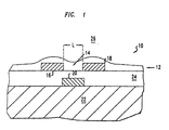
- FIG. 1 is a cross-sectional view of an organic field-effect-transistor (OFET) 10 whose electrical properties are sensitive to the presence of odors.
- the OFET 10 has an organic semiconductor layer 12 with a thickness of about 10-100 nanometers (nm).
- the organic semiconductor layer 12 forms an outer covering of the OFET 10 and includes an active channel 14.
- the OFET 10 also includes source 16, drain 18, and gate 20.
- the gate 20 rests on a silicon substrate 22 and is insulated from the organic semiconductor layer 12, source 16, and drain 18 by a dielectric layer 24.
- the active channel 14 refers to the portion of layer 12 located between the source 16 and drain 18.
- a voltage applied to gate 20 controls the conductivity of the active channel 14.
- the voltage on the gate 20 controls the conductivity of an active portion of the channel 14 adjacent to the dielectric layer 24, e.g., a few molecules thick.
- the silicon substrate 22 also functions as the gate.
- the channel 14 formed in the layer 12 is able to absorb odor molecules from ambient gas 26. Absorption of certain odor molecules changes the conductivity of active channel 14 by changing carrier densities, trap densities, mobilities, or another property of the organic semiconductor layer 12. Changing the channel's conductivity changes the drain current in the channel 14. Thus, changes in the drain current are electrical responses to the presence of odor molecules in ambient gas 26 above the unprotected layer 12 and characterize OFET 10 as an electronic odor sensor.
- the odor-sensitivity of OFET 10 depends on both the physical structure and the chemical composition of active layer 12.
- Organic semiconductor layer 12 has a polycrystalline structure in which grains have diameters of about 10-100 nm. These small grain sizes facilitate penetration of odor molecules into the layer 12 by making a high surface area available for odor penetration. These effects of small grain sizes facilitate chemical and/or physical interaction between odor molecules and molecules of active channel 14 and ordinarily increase the odor-sensitivity of the OFET 10.
- the active layer 12 includes a stable organic semiconductor such as a material made of organic molecules with conjugated double bonds.
- exemplary organic semiconductors include hydrocarbon-end-substituted ⁇ -sexithiophene ( ⁇ -6T), hydrocarbon-substituted polymers of thiophene, 1,4,5,8-naphthalene tetracarboxylic dianhydride (NTCDA), copper phthalocyanine (CuPc), and a metal-hexadecafluoro-phthalocyanine (F 16 MPc).
- Exemplary semiconductors based on ⁇ -6T include di-hexyl- ⁇ -6T (dH ⁇ 6T), di-butyl- ⁇ -6T(dB ⁇ 6T), di-dodecyl- ⁇ -6T (dDD ⁇ 6T), and di-octadecyl- ⁇ -6T (dOD ⁇ 6T).
- Exemplary semiconductors based on polymers of thiophene include regioregular poly-hexyl-thiophene (pHT), poly-dodecyl-thiophene (pDDT), and poly-octyl-thiophene (pOT).
- the semiconductors based on F 16 MPc include molecules in which the metal atom "M" is copper, zinc, iron, or cobalt.
- the odor-sensitivity of OFET 10 also depends on the types of hydrocarbon end-groups on molecules of organic semiconductor layer 12 and on the sizes of the odor molecules. Both of these properties affect penetration depths of the odor molecules into the active channel 14. If the active channel 14 is composed of molecules with larger hydrocarbon end-groups, the corresponding OFET 10 ordinarily has a higher sensitivity due to higher penetration of the odor molecules.
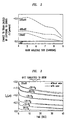
- Figure 2 graphs the change to the drain current, i.e., ⁇ I on , which results from exposure to an odor, for OFETs 10 that have semiconductor layers 12 of different molecular compositions.
- the molecules of the different organic semiconductor layers 12 have different hydrocarbon end-groups.
- the responsiveness of the change to the drain current ⁇ I on to presence of the alcohol odor molecules increases as lengths of the hydrocarbon end-groups of the molecules increase.
- an OFET 10 is more sensitive to odor molecules if its organic semiconductor layer 12 includes molecules with larger hydrocarbon end-groups.
- FIG. 3 illustrates the time-dependence of the drain current I d as a function of time for various gate-source voltages V g .
- the drain current I d depends on time even when odor molecules are not present.
- Figure 3 shows the drain current I d both for calibration periods in which odor molecules are absent and for test periods in which odor molecules are present.
- odor molecules of 1-octanol are present in ambient gas 26 and diffuse into the active channel 14 of dD ⁇ 6T.
- ambient gas 26 carries 1-octanol molecules during a 10 second period that starts about ten seconds after OFET 10 is powered to produce a drain current.
- the value of the drain current I d starts to deviate from the value of the drain current for corresponding times in the calibration periods in which 1-octanol odor molecules are absent.
- the size of the deviation between the drain currents I d of the test and calibration periods depends on both the biasing voltage V g and the time that the OFET's semiconductor channel is exposed to the 1-octanol odor. For Vg more negative than -1.0 volts, the deviation ⁇ I d between the drain currents is measurable after about 5 seconds of exposure to the 1-octanol odor molecules. This delay is caused by the time it takes for 1-octanol molecules to diffuse into the organic semiconductor channel 14.
- the deviation ⁇ I d in drain current is an electrical response to the presence of odor molecules, i.e., presence of the odor molecules has altered the electrical properties of the OFET 10.
- the size of the response also depends on the gate-source voltage V g .
- Figure 4 shows how the drain current of OFET 10 with an uncovered semiconductor layer 12 of dDD ⁇ T deviates in response to the presence of various odor molecules for different values of the gate-source voltages V g .
- the deviations are measured through the difference I t-d 1 ⁇ 2 - I c-d 1 ⁇ 2 where I t-d and I c-d are values of the drain current I d during equivalent temporal intervals of the respective calibration and test periods.
- the OFET 10 is not exposed to the odor.
- the OFET 10 is exposed to the odor, and the drain current is measured after a 5-second exposure of the OFET 10 to the odor.
- the difference I t-d 1 ⁇ 2 - I c-d 1 ⁇ 2 vanishes for odors that do not produce a response in electrical properties of the OFET 10.
- the measurements of Figure 4 illustrate that relative responses of the drain current to various odors are also affected by gate-source voltage V g .
- V g gate-source voltage
- the set of values of I t-d 1 ⁇ 2 - I c-d 1 ⁇ 2 that corresponds to a set of values of the gate-source voltages, e.g., for ⁇ V g ⁇ (-0, -1.0, -2.0, -3.0, -4.0), provides a vector-valued "fingerprint".
- the set values of I t- d 1 ⁇ 2 - I c-d 1 ⁇ 2 is a fingerprint, because the set of values is usable to identify and distinguish between the presence of the different odor molecules listed in Figure 4.
- the set of values of I t-d 1 ⁇ 2 - I c-d 1 ⁇ 2 are different for different odor molecules, because sensitivities of organic semiconductor layer 12 to odors vary when biased by different gate voltages V g .
- This type of normalization produces a vector-object that identifies an odor in a manner that does not depend on the concentration of the odor molecules. For such a vector, the pattern formed by the magnitudes of the components distinguishes between different types of odor molecules.
- the various odor molecules cause different deviations in the drain currents I d for OFETs 10 with active layers of different compositions.
- an array of OFETs 10 with active layers 12 of different compositions respond to exposure to odors by a set of drain current deviations ⁇ I d , and the set of ⁇ I d 's identify and distinguish between the odors.
- the array of drain current deviations ⁇ I d for OFETs 10 whose active layers 12 comprise dH ⁇ 6T, dDD ⁇ 6T, dOD ⁇ 6T, and CuPc provides a vector-like set of current deviations that identifies and distinguishes between toluene, 1-carvone, eugenol, and vanillin.
- an object identifies and distinguishes between the presence of first and second odors if the object has a value associated with the first odor and a value associated with the second odor and the two values are different.
- one such object is the orientation of the 5-dimensional vector of values of ⁇ I d produced by OFETs with dH ⁇ 6T, dDD ⁇ 6T, dOD ⁇ 6T, and CuPc active channels 14.
- Figure 6 shows an electronic array-type odor sensor 40.
- the array-type sensor 40 includes N odor-sensitive voltage amplifiers 42 1 - 42 N having respective input terminals 44 1 - 44 N , output terminals 46 1 - 46 N , and power terminals 48 1 - 48 N , 50 1 -50 N .
- the input terminals 46 1 - 46 N connect to voltage divider circuits 52 1 - 52 N that apply input voltages to the amplifiers 42 1 - 42 N . These input voltages may be DC or pulsed.
- the output terminals 46 1 - 46 N connect to input terminals 54 1 - 54 N of a comparator device 56, which measures the output voltages V out-1 - V out-N and determines the identity of an odor from the measured values of the output voltages V out-1 - V out-N .
- the array-type sensor 40 performs parallel accumulation and analysis of the set of output voltages V out-1 - V out-N , which are used to identify and distinguish between odors. Accumulating the set of output voltages in parallel speeds up odor detection, because the measurement process for individual output voltages involves test periods that are from about 1 to about 40 seconds long.
- the different amplifiers 42 1 - 42 N have organic semiconductor layers 53 1 -53 N with field-induced conductivities that respond differently to the presence of odors.
- the set of output voltages V out-1 - V out-N from the amplifiers 42 1 - 42 N also responds to the conductivities of the layers 53 1 - 53 N . Due to differences between responses of the conductivities of the layers 53 1 -53 N to different odors, the set of output voltages V out-1 - V out-N takes different values for different odors.
- the conductivities of the layers 53 1 - 53 N also respond to the values of the input voltages applied to input terminals 44 1 - 44 N .
- the set of output voltages V out-1 -V out-N forms an N-dimensional vector whose direction in N-dimensional space identifies and distinguishes between different odors due to the differences in the responses of the conductivities of layers 53 1 - 53 N to the odors.
- the comparator device 56 compares the set of N output voltages V out-1 -V out-N to reference sets of output voltages for matches.
- the values of the reference sets correspond to the output voltages V out-1 -V out-N generated by the amplifiers 42 1 - 42 N in response to the presence of known odors.
- a data storage device 58 connected to the comparator device 56 stores the values of the reference sets.
- Exemplary data storage devices 58 include an active memory, a magnetic disk, or an optical disk.
- Exemplary comparator devices 56 include a computer that executes a software program, e.g., a computer executable program stored on an optical or magnetic disk.
- the program performs a process for measuring the set of output voltages V out-1 - V out-N at terminals 54 1 - 54 N , comparing the measured set of output voltages to reference sets stored in the data storage device 58, and determining the identity of an odor molecule from the comparison.
- FIG. 7A shows an exemplary voltage amplifier 42A for use as odor-sensitive amplifiers 42 1 - 42 N of Figure 1.
- odor-sensitive OFET 10 of Figure 1 and load resistor 60 form a series circuit between V D and ground voltage sources.
- the OFET's gate 20 and drain 18 connect to respective input and output terminals 44, 46.
- the input voltage V IN biases the OFET 10
- the OFET's drain voltage is the output voltage V OUT of the amplifier 42A.
- the output voltage V OUT is responsive to the conductivity of the OFET's active channel, i.e., channel 14 of Figure 1.
- the conductivity is responsive both to the presence of odors in ambient gas 26 and to the voltage V IN at input terminal 44.
- the value of the drain voltage V OUT and drain current of the OFET 10 are responsive to the presence of odors.
- Figure 7B shows an alternate voltage amplifier 42B for use as odor sensitive amplifiers 42 1 - 42 N of Figure 6.
- the amplifier 42B has two cascaded stages. Each stage includes a load resistor 60A, 60B connected in series with a drain or source of an odor-sensitive OFET 10A, 10B. The stages connect between V D and ground voltage sources.
- the OFET 10B of the first stage has a gate 20B biased by voltage V IN at input terminal 44, i.e., input terminals 44 1 - 44 N in Figure 6, and a drain 18B that biases the gate 20A of the OFET 10A of the second stage in a cascade-like configuration.
- the drain 18A of the OFET 10A of the second stage connects to output terminal 46 of the amplifier 42B.
- Both OFETs 10A, 10B have organic semiconductor channels with conductivities that are responsive to the input voltage V IN and to the presence of odors in ambient gas.
- the cascaded arrangement of the odor-sensitive OFETs 10A, 10B makes the output voltage V OUT more sensitive to odors, because the output voltage of the odor-sensitive first stage is amplified by the odor-sensitive second stage.
- the voltage gain of the odor sensitive amplifiers are not essential. Some exemplary amplifiers have voltage gains greater than 1 and other exemplary amplifiers have voltage gains less than or equal to 1.
- the odor-sensitive amplifiers 42 1 - 42 N have different sensitivities to various odors so that the output voltages V out-1 -Vout-N provide a pattern of voltage values for distinguishing between different odors.
- the different sensitivities of the amplifiers 42 1 - 42 N result from different biasing voltages applied at input terminals 44 1 - 44 N .
- the N voltage divider circuits 52 1 -52 N have resistors R 1 -R N with different values.
- the different sensitivities of the amplifiers 42 1 -42 N result from using OFETs 10 in different ones of the amplifiers 42 1 - 42 N .
- the different OFETs 10 have active channels 14 with either different organic semiconductors, different grain sizes, or different channel depths, i.e., different thicknesses of organic semiconductor layer 12 of Figure 1.
- Figure 8A is a flow chart for a process 70 that identifies odor molecules using an electronic array-type odor sensor 40 of Figure 6.
- the process 70 has a calibration phase and a test phase.
- the process 70 includes applying selected input voltages to and powering the odor-sensitive amplifiers 42 1 -42 N that generate sets of output voltages V OUT-1 - V OUT-N responsive to small changes in the input voltages (step 71).
- the selected input voltages applied to the odor-sensitive amplifiers 42 1 - 42 N have different values so that the individual amplifiers 42 1 - 42 N have different sensitivities to odor molecules.
- the process 70 includes measuring the output voltages without subjecting the odor-sensitive amplifiers 42 1 - 42 N to odor molecules (step 72). After measuring the output voltages, the process 70 includes reversing the input voltages so that the output voltages from odor-sensitive amplifiers 42 1 - 42 N are freed of effects of the previous input voltages (step 73). For the odor-sensitive amplifiers 42A, 42B of Figures 7A and 7B, reversing the input voltages causes the conductivities of active channels 14 of the OFETs 10, 10A, 10B to recover to pretest initial values for a given bias condition.
- the process 70 includes again powering the odor-sensitive amplifiers 42 1 - 42 N and reapplying the same selected input voltages to the amplifiers 42 1 - 42 N (step 74). At a preselected time thereafter, the process 70 includes passing gas, which carries odor molecules, over the odor-sensitive amplifiers 42 1 - 42 N so that the odor molecules are absorbed into active layers 14 therein (step 75).
- the process 70 includes measuring the output voltages produced by the odor-sensitive amplifiers 42 1 - 42 N (step 76).
- the process 70 includes using differences between the output voltages measured during the test and calibration phases to identify the odor molecules present and to determine concentrations of the odor molecules (step 77). By basing odor sensing on the differences between the output voltages measured in the calibration and test phases, background effects such as the drain current drift shown in Figure 3 are eliminated.
- the process 70 includes performing a recovery operation that reinitializes the odor-sensitive amplifiers for another sensing cycle with a new odor (step 78).
- the recovery operation includes passing odor-free gas over the amplifiers 42 1 - 42 N to outgas odor molecules bound in the organic semiconductor channels 14 and reversing input voltages to the odor-sensitive amplifiers 42 1 - 42 N during the outgasing as previously described. Some embodiments heat amplifiers 42 1 - 42 N to about 100°C to outgas odor molecules during the recovery operation.
- the carrier densities and chemical composition of the odor-sensitive organic semiconductor layers of the amplifiers 42 1 - 42 N are returned to their initial state. Then, the odor sensor 40 is ready to perform another sensing cycle for a new odor.
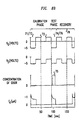
- Figure 8A illustrates an exemplary operation cycle of process 70 of Figure 8A.
- the cycle includes a calibration phase, a test phase, and a recovery operation.
- gate-source voltages V g gate-source voltages V D , drain-source voltages V D , drain currents I d , and concentrations of odor molecules are shown.
- Figure 9 is a flow chart for the step 77 in which odor molecules are identified based on the measured output voltages.
- comparator device 56 performs the identification step.
- the comparator device 56 forms a vector-like set of measured difference voltages by subtracting the set of output voltages measured in the calibration phase from the set of output voltages measured in the test phase (step 82).
- the components of the vector of measured difference voltages are indicative of changes to the array of amplifiers 42 1 - 42 N , which are caused by the presence of odors.
- the comparator device 56 looks for a match between the vector of measured difference voltages and reference vectors of difference voltages that correspond to known odor molecules (step 84).
- the values of the reference vectors of difference voltages are stored in data storage device 58 of Figure 6.
- the comparator device 56 performs a pattern recognition algorithm that signals a match in response to two compared N-component vectors pointing in the same direction in N-dimensional space, i.e., up to a preselected error.
- the pattern recognition algorithm is capable of signaling a match between vectors with different lengths.
- the comparator device 56 identifies the odor detected by the array-type sensor 40 as the known odor corresponding to the matching reference set (step 86).
- the comparator device 56 also determines the concentration of the odor by comparing values of one component of the set of measured difference voltages and to the same component of the matching reference set. Since the measured voltage differences are proportional to the concentration of odor molecules, the ratio of the value of one measured component to the value of the same component for the matching reference set measures the concentration of odor molecules.
- OFET 10 have active channels 14 whose physical dimensions, i.e., wide and length, have widely different sizes.
- some OFETs 10 have a channel 14 whose length L that is less than 20 nanometers.
- the response of the OFET can be more directly related to interactions between the organic semiconductor and analyte molecules. This may improve the sensitivity of an analyte sensor that uses such OFETs 10 as compared to a sensor that uses OFETs 10 with much longer channels.
Landscapes
- Chemical & Material Sciences (AREA)
- Life Sciences & Earth Sciences (AREA)
- Engineering & Computer Science (AREA)
- Health & Medical Sciences (AREA)
- Microelectronics & Electronic Packaging (AREA)
- Pathology (AREA)
- Immunology (AREA)
- Physics & Mathematics (AREA)
- Analytical Chemistry (AREA)
- Biochemistry (AREA)
- General Health & Medical Sciences (AREA)
- General Physics & Mathematics (AREA)
- Medicinal Chemistry (AREA)
- Food Science & Technology (AREA)
- Computer Hardware Design (AREA)
- Combustion & Propulsion (AREA)
- Molecular Biology (AREA)
- Chemical Kinetics & Catalysis (AREA)
- Electrochemistry (AREA)
- Investigating Or Analyzing Materials By The Use Of Electric Means (AREA)
- Investigating Or Analyzing Materials By The Use Of Fluid Adsorption Or Reactions (AREA)
Applications Claiming Priority (2)
| Application Number | Priority Date | Filing Date | Title |
|---|---|---|---|
| US09/793,642 US6575013B2 (en) | 2001-02-26 | 2001-02-26 | Electronic odor sensor |
| US793642 | 2001-02-26 |
Publications (2)
| Publication Number | Publication Date |
|---|---|
| EP1235070A1 EP1235070A1 (en) | 2002-08-28 |
| EP1235070B1 true EP1235070B1 (en) | 2004-05-26 |
Family
ID=25160436
Family Applications (1)
| Application Number | Title | Priority Date | Filing Date |
|---|---|---|---|
| EP01307701A Expired - Lifetime EP1235070B1 (en) | 2001-02-26 | 2001-09-11 | Electronic odor sensor |
Country Status (4)
| Country | Link |
|---|---|
| US (1) | US6575013B2 (enExample) |
| EP (1) | EP1235070B1 (enExample) |
| JP (1) | JP4104343B2 (enExample) |
| DE (1) | DE60103493T2 (enExample) |
Families Citing this family (40)
| Publication number | Priority date | Publication date | Assignee | Title |
|---|---|---|---|---|
| US6852996B2 (en) * | 2002-09-25 | 2005-02-08 | Stmicroelectronics, Inc. | Organic semiconductor sensor device |
| US6862917B2 (en) * | 2002-09-30 | 2005-03-08 | Bae Systems Information And Electronic Systems Integration Inc. | Apparatus for detecting chemical agents including olfactory interferometric lens and method of use |
| JP2006090983A (ja) * | 2004-09-27 | 2006-04-06 | Univ Of Tokyo | 面状素子モジュールおよびその製造方法並びに面状素子装置 |
| US7333604B2 (en) * | 2005-01-10 | 2008-02-19 | Infone Tech, Ltd. | Adaptive notification of an incoming call in a mobile phone |
| WO2006105077A2 (en) * | 2005-03-28 | 2006-10-05 | Massachusetts Institute Of Technology | Low voltage thin film transistor with high-k dielectric material |
| WO2007010425A1 (en) * | 2005-07-19 | 2007-01-25 | Koninklijke Philips Electronics N.V. | Fluid analyser |
| US7397072B2 (en) * | 2005-12-01 | 2008-07-08 | Board Of Regents, The University Of Texas System | Structure for and method of using a four terminal hybrid silicon/organic field effect sensor device |
| US20070215863A1 (en) * | 2006-03-15 | 2007-09-20 | Lucent Technologies Inc. | Fabricating apparatus with doped organic semiconductors |
| US8384409B2 (en) * | 2007-05-03 | 2013-02-26 | The Regents Of The University Of California | Ultra-thin organic TFT chemical sensor, making thereof, and sensing method |
| DE102007029153A1 (de) | 2007-06-25 | 2009-01-08 | Robert Bosch Gmbh | Halbleitergassensor mit zusätzlichen Funktionalitäten der signalbildenden Elektrode |
| DE102007034331A1 (de) | 2007-07-24 | 2009-01-29 | Robert Bosch Gmbh | Vorrichtung und Verfahren zur Detektierung von Substanzen |
| US8178357B2 (en) * | 2007-07-26 | 2012-05-15 | The Regents Of The University Of California | Peroxide chemical sensor and sensing method |
| FR2922310B1 (fr) * | 2007-10-15 | 2012-05-11 | Univ Pierre Et Marie Curie Paris Vi | Transducteur a semi conducteurs,et son utilisation dans un capteur d'especes donneuses ou acceptrices d'electrons. |
| JP5056398B2 (ja) * | 2007-12-19 | 2012-10-24 | 株式会社豊田中央研究所 | センサの使用方法及びセンサ装置 |
| US7821000B2 (en) | 2008-02-01 | 2010-10-26 | Alcatel-Lucent Usa Inc. | Method of doping organic semiconductors |
| US8955765B2 (en) * | 2008-08-20 | 2015-02-17 | S.C. Johnson & Son, Inc. | Diffusion device with odor sensor |
| AT14040U1 (de) * | 2009-04-09 | 2015-03-15 | Ullstein Hanns Jun | Reinigungsgerät für pferdeställe |
| US8438904B2 (en) | 2010-05-03 | 2013-05-14 | Sensorbit Systems, Inc. | Method and apparatus for vapor signature with heat differential |
| US8816149B2 (en) | 2011-10-28 | 2014-08-26 | Kimberly-Clark Worldwide, Inc. | System for detection and monitoring of body exudates using a gas emitting substance for use in interactive toilet training |
| US9119748B2 (en) * | 2011-10-28 | 2015-09-01 | Kimberly-Clark Worldwide, Inc. | Electronic discriminating device for body exudate detection |
| US8933292B2 (en) | 2011-10-28 | 2015-01-13 | Kimberly-Clark Worldwide, Inc. | Absorbent article with sensor array for body exudate detection |
| CN109071212A (zh) * | 2016-01-28 | 2018-12-21 | 罗斯韦尔生物技术股份有限公司 | 使用大规模分子电子传感器阵列测量分析物的方法和装置 |
| KR102609959B1 (ko) * | 2016-10-05 | 2023-12-06 | 엘지전자 주식회사 | 가스 센서 |
| US10816519B1 (en) * | 2017-07-18 | 2020-10-27 | Volatile Analysis Corporation | Systems and methods for analyzing odors |
| EP3962407A4 (en) | 2019-04-30 | 2023-04-19 | Smylio Inc. | BUCCAL APPLIANCE SUPPORT |
| GB201915639D0 (en) * | 2019-10-29 | 2019-12-11 | P E S Tech Limited | A sensor |
| WO2021199893A1 (ja) | 2020-04-02 | 2021-10-07 | I-Pex株式会社 | 匂い検出システム、匂い検出方法及びプログラム |
| US11932080B2 (en) | 2020-08-20 | 2024-03-19 | Denso International America, Inc. | Diagnostic and recirculation control systems and methods |
| US11828210B2 (en) | 2020-08-20 | 2023-11-28 | Denso International America, Inc. | Diagnostic systems and methods of vehicles using olfaction |
| US11881093B2 (en) | 2020-08-20 | 2024-01-23 | Denso International America, Inc. | Systems and methods for identifying smoking in vehicles |
| US11760169B2 (en) | 2020-08-20 | 2023-09-19 | Denso International America, Inc. | Particulate control systems and methods for olfaction sensors |
| US12269315B2 (en) | 2020-08-20 | 2025-04-08 | Denso International America, Inc. | Systems and methods for measuring and managing odor brought into rental vehicles |
| US11760170B2 (en) | 2020-08-20 | 2023-09-19 | Denso International America, Inc. | Olfaction sensor preservation systems and methods |
| US12251991B2 (en) | 2020-08-20 | 2025-03-18 | Denso International America, Inc. | Humidity control for olfaction sensors |
| US12017506B2 (en) | 2020-08-20 | 2024-06-25 | Denso International America, Inc. | Passenger cabin air control systems and methods |
| US11636870B2 (en) | 2020-08-20 | 2023-04-25 | Denso International America, Inc. | Smoking cessation systems and methods |
| US12377711B2 (en) | 2020-08-20 | 2025-08-05 | Denso International America, Inc. | Vehicle feature control systems and methods based on smoking |
| US11813926B2 (en) | 2020-08-20 | 2023-11-14 | Denso International America, Inc. | Binding agent and olfaction sensor |
| US12467913B2 (en) * | 2022-01-26 | 2025-11-11 | Clifford B. Zlotnik | Portable odor detection system |
| CN115326887B (zh) * | 2022-07-25 | 2025-07-25 | 武汉轻工大学 | 有机场效应晶体管气敏传感器、气味测量电路以及方法 |
Citations (1)
| Publication number | Priority date | Publication date | Assignee | Title |
|---|---|---|---|---|
| US6085576A (en) * | 1998-03-20 | 2000-07-11 | Cyrano Sciences, Inc. | Handheld sensing apparatus |
Family Cites Families (28)
| Publication number | Priority date | Publication date | Assignee | Title |
|---|---|---|---|---|
| US3831432A (en) | 1972-09-05 | 1974-08-27 | Texas Instruments Inc | Environment monitoring device and system |
| DE2407110C3 (de) * | 1974-02-14 | 1981-04-23 | Siemens AG, 1000 Berlin und 8000 München | Sensor zum Nachweis einer in einem Gas oder einer Flüssigkeit einthaltenen Substanz |
| DE2947050C2 (de) | 1979-11-22 | 1992-11-26 | Karoly Dr. 4600 Dortmund Dobos | Anordnung zum Nachweis von Ionen, Atomen und Molekülen in Gasen oder Lösungen |
| JPS619288A (ja) * | 1984-06-21 | 1986-01-16 | Dai Ichi Seiyaku Co Ltd | ペプチド類の製法 |
| US4730479A (en) | 1986-06-23 | 1988-03-15 | The Standard Oil Company | Temperature and humidity compensation for gas detection apparatus |
| DE3642891A1 (de) | 1986-12-16 | 1988-06-30 | Fraunhofer Ges Forschung | Sensoranordnung zum nachweis der konzentration einer oder mehrerer komponenten in einem gasgemisch durch reihenschaltung zweier oder mehrerer gasempfindlicher feldeffekttransistoren |
| GB8708201D0 (en) * | 1987-04-06 | 1987-05-13 | Cogent Ltd | Gas sensor |
| US5200634A (en) * | 1988-09-30 | 1993-04-06 | Hitachi, Ltd. | Thin film phototransistor and photosensor array using the same |
| DE4028062C2 (de) | 1990-09-05 | 1994-09-22 | Winter Gaswarnanlagen Gmbh U | Gassensoranordnung mit FET mit unterbrochenem Gate |
| US5159661A (en) | 1990-10-05 | 1992-10-27 | Energy Conversion Devices, Inc. | Vertically interconnected parallel distributed processor |
| JPH04181150A (ja) * | 1990-11-15 | 1992-06-29 | Kaoru Santo | 脂質膜型匂いセンサ |
| JPH05312746A (ja) * | 1992-05-06 | 1993-11-22 | Mitsubishi Electric Corp | 臭気センサー |
| GB9412633D0 (en) * | 1994-06-23 | 1994-08-10 | Aromascan Plc | Semiconducting organic polymers |
| GB9412632D0 (en) * | 1994-06-23 | 1994-08-10 | Aromascan Plc | Semiconducting organic polymers |
| GB9425207D0 (en) * | 1994-12-14 | 1995-02-15 | Aromascan Plc | Semi-conducting organic polymers |
| GB9523406D0 (en) | 1995-11-16 | 1996-01-17 | Aromascan Plc | Sensor transduction |
| JPH1071323A (ja) * | 1996-08-30 | 1998-03-17 | Aqueous Res:Kk | 空気浄化フィルタ及び自動車用空気浄化装置 |
| GB9705278D0 (en) | 1997-03-14 | 1997-04-30 | Aromascan Plc | Gas sensor |
| EP0878711A1 (en) * | 1997-05-15 | 1998-11-18 | Interuniversitair Micro-Elektronica Centrum Vzw | Chemically sensitive sensor comprising arylene alkenylene oligomers |
| JPH1119454A (ja) * | 1997-06-30 | 1999-01-26 | Sanyo Electric Co Ltd | 脱臭装置 |
| WO1999008105A1 (en) | 1997-08-08 | 1999-02-18 | California Institute Of Technology | Techniques and systems for analyte detection |
| DE19753300A1 (de) * | 1997-12-01 | 1999-06-02 | Basf Ag | Verfahren zur Herstellung von festen Dosierungsformen |
| WO1999061902A1 (en) | 1998-05-27 | 1999-12-02 | California Institute Of Technology | Method of resolving analytes in a fluid |
| JP2002518668A (ja) * | 1998-06-19 | 2002-06-25 | カリフォルニア インスティチュート オブ テクノロジー | 人工の嗅覚検査を用いた極微量の分析物の検出 |
| US6207472B1 (en) * | 1999-03-09 | 2001-03-27 | International Business Machines Corporation | Low temperature thin film transistor fabrication |
| US6284562B1 (en) * | 1999-11-17 | 2001-09-04 | Agere Systems Guardian Corp. | Thin film transistors |
| JP2001284592A (ja) * | 2000-03-29 | 2001-10-12 | Sony Corp | 薄膜半導体装置及びその駆動方法 |
| GB0008019D0 (en) * | 2000-03-31 | 2000-05-17 | Koninkl Philips Electronics Nv | Display device having current-addressed pixels |
-
2001
- 2001-02-26 US US09/793,642 patent/US6575013B2/en not_active Expired - Lifetime
- 2001-09-11 DE DE60103493T patent/DE60103493T2/de not_active Expired - Lifetime
- 2001-09-11 EP EP01307701A patent/EP1235070B1/en not_active Expired - Lifetime
-
2002
- 2002-02-20 JP JP2002042898A patent/JP4104343B2/ja not_active Expired - Fee Related
Patent Citations (1)
| Publication number | Priority date | Publication date | Assignee | Title |
|---|---|---|---|---|
| US6085576A (en) * | 1998-03-20 | 2000-07-11 | Cyrano Sciences, Inc. | Handheld sensing apparatus |
Also Published As
| Publication number | Publication date |
|---|---|
| DE60103493T2 (de) | 2005-06-23 |
| US20020116983A1 (en) | 2002-08-29 |
| US6575013B2 (en) | 2003-06-10 |
| DE60103493D1 (de) | 2004-07-01 |
| EP1235070A1 (en) | 2002-08-28 |
| JP4104343B2 (ja) | 2008-06-18 |
| JP2002310969A (ja) | 2002-10-23 |
Similar Documents
| Publication | Publication Date | Title |
|---|---|---|
| EP1235070B1 (en) | Electronic odor sensor | |
| US6521109B1 (en) | Device for detecting an analyte in a sample based on organic materials | |
| US10132773B2 (en) | Using floating gate field effect transistors for chemical and/or biological sensing | |
| EP1085319B1 (en) | A device for detecting an analyte in a sample based on organic materials | |
| Gusain et al. | Flexible NO gas sensor based on conducting polymer poly [N-9′-heptadecanyl-2, 7-carbazole-alt-5, 5-(4′, 7′-di-2-thienyl-2′, 1′, 3′-benzothiadiazole)](PCDTBT) | |
| Tanese et al. | Interface and gate bias dependence responses of sensing organic thin-film transistors | |
| Kumar et al. | Flexible poly (3, 3′′′-dialkylquaterthiophene) based interdigitated metal-semiconductor-metal ammonia gas sensor | |
| Rahmanudin et al. | Robust high‐capacitance polymer gate dielectrics for stable low‐voltage organic field‐effect transistor sensors | |
| Janata et al. | Organic semiconductors in potentiometric gas sensors | |
| JP2002310969A5 (enExample) | ||
| US10481126B2 (en) | Electrolyte-gated transistors for detection of molecules | |
| Shkodra et al. | Optimization of the spray-deposited carbon nanotube semiconducting channel for electrolyte-gated field-effect transistor-based biosensing applications | |
| Janata | Electrochemical microsensors | |
| Barker et al. | A polyaniline/sllicon hybrid field effect transistor humidity sensor | |
| Li et al. | Subthreshold-operated low-voltage organic field-effect transistor for ion-sensing system of high transduction sensitivity | |
| Bausells et al. | On the impedance spectroscopy of field‐effect biosensors | |
| Massey et al. | Label-free detection of dopamine using aptamer enhanced organic-electrolyte gated FET sensor | |
| An et al. | Study on the Effect of the Electrode Structure of an ITO Nanoparticle Film Sensor On Operating Performance | |
| Minami et al. | Chemical sensing based on water-gated polythiophene thin-film transistors | |
| Liangyan et al. | A gas sensor fabricated with field-effect transistors and Langmuir-Blodgett film of porphyrin | |
| CN118348093A (zh) | 一种基于多通道场效应晶体管的生物传感器及制备方法 | |
| KR100918025B1 (ko) | 검출 소자 | |
| Barker et al. | Electrical characteristics of a polyaniline/silicon hybrid field-effect transistor gas sensor | |
| Diallo et al. | Influence of temperature and pentacene thickness on the electrical parameters in top gate organic thin film transistor | |
| Cheng et al. | Improved performance of highly sensitive room-temperature ammonia gas sensor with P-type doping carbazole-triazine derivative |
Legal Events
| Date | Code | Title | Description |
|---|---|---|---|
| PUAI | Public reference made under article 153(3) epc to a published international application that has entered the european phase |
Free format text: ORIGINAL CODE: 0009012 |
|
| 17P | Request for examination filed |
Effective date: 20010920 |
|
| AK | Designated contracting states |
Kind code of ref document: A1 Designated state(s): AT BE CH CY DE DK ES FI FR GB GR IE IT LI LU MC NL PT SE TR |
|
| AX | Request for extension of the european patent |
Free format text: AL;LT;LV;MK;RO;SI |
|
| 17Q | First examination report despatched |
Effective date: 20021022 |
|
| AKX | Designation fees paid |
Designated state(s): DE FR GB |
|
| GRAP | Despatch of communication of intention to grant a patent |
Free format text: ORIGINAL CODE: EPIDOSNIGR1 |
|
| GRAS | Grant fee paid |
Free format text: ORIGINAL CODE: EPIDOSNIGR3 |
|
| GRAA | (expected) grant |
Free format text: ORIGINAL CODE: 0009210 |
|
| AK | Designated contracting states |
Kind code of ref document: B1 Designated state(s): DE FR GB |
|
| REG | Reference to a national code |
Ref country code: GB Ref legal event code: FG4D |
|
| REG | Reference to a national code |
Ref country code: IE Ref legal event code: FG4D |
|
| REF | Corresponds to: |
Ref document number: 60103493 Country of ref document: DE Date of ref document: 20040701 Kind code of ref document: P |
|
| ET | Fr: translation filed | ||
| PLBE | No opposition filed within time limit |
Free format text: ORIGINAL CODE: 0009261 |
|
| STAA | Information on the status of an ep patent application or granted ep patent |
Free format text: STATUS: NO OPPOSITION FILED WITHIN TIME LIMIT |
|
| 26N | No opposition filed |
Effective date: 20050301 |
|
| REG | Reference to a national code |
Ref country code: IE Ref legal event code: MM4A |
|
| REG | Reference to a national code |
Ref country code: GB Ref legal event code: 732E Free format text: REGISTERED BETWEEN 20131031 AND 20131106 |
|
| REG | Reference to a national code |
Ref country code: FR Ref legal event code: CD Owner name: ALCATEL-LUCENT USA INC. Effective date: 20131122 |
|
| REG | Reference to a national code |
Ref country code: FR Ref legal event code: GC Effective date: 20140410 |
|
| REG | Reference to a national code |
Ref country code: FR Ref legal event code: RG Effective date: 20141015 |
|
| REG | Reference to a national code |
Ref country code: FR Ref legal event code: PLFP Year of fee payment: 15 |
|
| REG | Reference to a national code |
Ref country code: FR Ref legal event code: PLFP Year of fee payment: 16 |
|
| REG | Reference to a national code |
Ref country code: FR Ref legal event code: PLFP Year of fee payment: 17 |
|
| REG | Reference to a national code |
Ref country code: FR Ref legal event code: PLFP Year of fee payment: 18 |
|
| PGFP | Annual fee paid to national office [announced via postgrant information from national office to epo] |
Ref country code: FR Payment date: 20180924 Year of fee payment: 18 Ref country code: DE Payment date: 20180920 Year of fee payment: 18 |
|
| PGFP | Annual fee paid to national office [announced via postgrant information from national office to epo] |
Ref country code: GB Payment date: 20180919 Year of fee payment: 18 |
|
| REG | Reference to a national code |
Ref country code: DE Ref legal event code: R119 Ref document number: 60103493 Country of ref document: DE |
|
| PG25 | Lapsed in a contracting state [announced via postgrant information from national office to epo] |
Ref country code: DE Free format text: LAPSE BECAUSE OF NON-PAYMENT OF DUE FEES Effective date: 20200401 |
|
| GBPC | Gb: european patent ceased through non-payment of renewal fee |
Effective date: 20190911 |
|
| PG25 | Lapsed in a contracting state [announced via postgrant information from national office to epo] |
Ref country code: FR Free format text: LAPSE BECAUSE OF NON-PAYMENT OF DUE FEES Effective date: 20190930 Ref country code: GB Free format text: LAPSE BECAUSE OF NON-PAYMENT OF DUE FEES Effective date: 20190911 |