EP1213827A2 - Überstrom-Erfassungseinrichtung - Google Patents
Überstrom-Erfassungseinrichtung Download PDFInfo
- Publication number
- EP1213827A2 EP1213827A2 EP01250429A EP01250429A EP1213827A2 EP 1213827 A2 EP1213827 A2 EP 1213827A2 EP 01250429 A EP01250429 A EP 01250429A EP 01250429 A EP01250429 A EP 01250429A EP 1213827 A2 EP1213827 A2 EP 1213827A2
- Authority
- EP
- European Patent Office
- Prior art keywords
- semiconductor component
- switched
- resistor
- emitter
- load
- Prior art date
- Legal status (The legal status is an assumption and is not a legal conclusion. Google has not performed a legal analysis and makes no representation as to the accuracy of the status listed.)
- Withdrawn
Links
- 238000001514 detection method Methods 0.000 title claims abstract description 18
- 239000004065 semiconductor Substances 0.000 claims abstract description 61
- 238000005259 measurement Methods 0.000 claims abstract description 33
- 230000006378 damage Effects 0.000 abstract description 5
- 230000003068 static effect Effects 0.000 description 5
- 238000010586 diagram Methods 0.000 description 4
- 230000005856 abnormality Effects 0.000 description 3
- 238000004458 analytical method Methods 0.000 description 3
- 230000000694 effects Effects 0.000 description 2
- 230000001681 protective effect Effects 0.000 description 2
- 238000010276 construction Methods 0.000 description 1
- 230000001419 dependent effect Effects 0.000 description 1
- 238000013461 design Methods 0.000 description 1
- 238000011161 development Methods 0.000 description 1
- 230000018109 developmental process Effects 0.000 description 1
- 238000004880 explosion Methods 0.000 description 1
- 238000003780 insertion Methods 0.000 description 1
- 230000037431 insertion Effects 0.000 description 1
- 230000002427 irreversible effect Effects 0.000 description 1
- 238000000691 measurement method Methods 0.000 description 1
- 239000000155 melt Substances 0.000 description 1
- 229920006395 saturated elastomer Polymers 0.000 description 1
- 238000009738 saturating Methods 0.000 description 1
Images






Classifications
-
- H—ELECTRICITY
- H02—GENERATION; CONVERSION OR DISTRIBUTION OF ELECTRIC POWER
- H02M—APPARATUS FOR CONVERSION BETWEEN AC AND AC, BETWEEN AC AND DC, OR BETWEEN DC AND DC, AND FOR USE WITH MAINS OR SIMILAR POWER SUPPLY SYSTEMS; CONVERSION OF DC OR AC INPUT POWER INTO SURGE OUTPUT POWER; CONTROL OR REGULATION THEREOF
- H02M7/00—Conversion of AC power input into DC power output; Conversion of DC power input into AC power output
- H02M7/42—Conversion of DC power input into AC power output without possibility of reversal
- H02M7/44—Conversion of DC power input into AC power output without possibility of reversal by static converters
- H02M7/48—Conversion of DC power input into AC power output without possibility of reversal by static converters using discharge tubes with control electrode or semiconductor devices with control electrode
- H02M7/53—Conversion of DC power input into AC power output without possibility of reversal by static converters using discharge tubes with control electrode or semiconductor devices with control electrode using devices of a triode or transistor type requiring continuous application of a control signal
- H02M7/537—Conversion of DC power input into AC power output without possibility of reversal by static converters using discharge tubes with control electrode or semiconductor devices with control electrode using devices of a triode or transistor type requiring continuous application of a control signal using semiconductor devices only, e.g. single switched pulse inverters
- H02M7/538—Conversion of DC power input into AC power output without possibility of reversal by static converters using discharge tubes with control electrode or semiconductor devices with control electrode using devices of a triode or transistor type requiring continuous application of a control signal using semiconductor devices only, e.g. single switched pulse inverters in a push-pull configuration
-
- H—ELECTRICITY
- H02—GENERATION; CONVERSION OR DISTRIBUTION OF ELECTRIC POWER
- H02M—APPARATUS FOR CONVERSION BETWEEN AC AND AC, BETWEEN AC AND DC, OR BETWEEN DC AND DC, AND FOR USE WITH MAINS OR SIMILAR POWER SUPPLY SYSTEMS; CONVERSION OF DC OR AC INPUT POWER INTO SURGE OUTPUT POWER; CONTROL OR REGULATION THEREOF
- H02M1/00—Details of apparatus for conversion
- H02M1/32—Means for protecting converters other than automatic disconnection
-
- H—ELECTRICITY
- H03—ELECTRONIC CIRCUITRY
- H03K—PULSE TECHNIQUE
- H03K17/00—Electronic switching or gating, i.e. not by contact-making and –breaking
- H03K17/08—Modifications for protecting switching circuit against overcurrent or overvoltage
- H03K17/082—Modifications for protecting switching circuit against overcurrent or overvoltage by feedback from the output to the control circuit
- H03K17/0828—Modifications for protecting switching circuit against overcurrent or overvoltage by feedback from the output to the control circuit in composite switches
Definitions
- the invention relates to the field of power electronics, in particular to the field of high current modules and an overcurrent detector, in particular for high-current modules with semiconductor components that can be switched off.
- a current sensor as an integral part contains.
- the current sensor consists of a resistor in series with an IGBT (insulated gate bipolar transistor or bipolar transistor with an insulated Gate electrode).
- JP 8195411 A1 It is also known from JP 8195411 A1 to use securing (melt) strips, to open a current current path in the event of a short circuit.
- EP 0 833 422 A2 discloses a protective circuit for a switchable Semiconductor device in which between each semiconductor device and an output terminal an irreversible short-circuit current limiter is formed which In the event of a short circuit, it melts. By breaking through the collector gate and emitter-gate junctions then lie both the gate of the semiconductor device in the path with melted short-circuit current limiter as well the associated gate of at least one semiconductor component lying in parallel for example on the full positive supply voltage. This will the intact semiconductor component is switched through and the in an intermediate circuit stored energy is derived from it. This is usually due to the still high currents also destroy the parallel semiconductor component result, however, an explosion of the entire circuit is prevented.
- JP 10257779 A1 it is known from JP 10257779 A1 to design an integrated power module, that with a gate electronics or a gate drive and a control device is integrated to detect abnormalities.
- This control device detects the presence of an abnormality from the output signals of a first comparator circuit that judges whether a detected voltage is close to that of a positive electrode, and a second comparator circuit that judges whether the detected voltage is close to that of a negative electrode, and the output of a Ignition signal, the switching on and off of a semiconductor element for switching controls.
- a switch-off circuit off.
- the present invention is therefore intended to provide an overcurrent detection device places where no measurement of the total current is required and still reliable results are achieved.
- the overcurrent detection device uses a current distribution between semiconductor components which can be switched off in parallel, for example IGBT components, in order to reduce the maximum current to be measured.
- a basic circuit with such a current distribution is shown in FIG. 9.
- five semiconductor components T 11 to T 15 which can be switched off for example transistors with an insulated gate (IGBT) are each arranged with a resistor R 11 to R 15 in front of the insulated gate connection.
- the collector connections of these transistors T 11 to T 15 are electrically connected to one another.
- One of the transistors with an insulated gate T 15 is used as a measuring transistor, behind whose emitter connection a protective device 11 is arranged.
- the current to be measured is significantly reduced.
- additional elements are always arranged in the emission path, so that they are at the same potential as the gate electronics or the gate drive.
- the following is a rapid overcurrent detection device according to the invention in the worst case, using only two Parallel semiconductor components that can be switched off using the example of IGBT components per branch, one of which is used for current measurement, described in more detail.
- FIG. 1 shows a circuit for current measurement in which a measuring IGBT T M1 , T M2 is connected in parallel to a load-carrying or load IGBT T L1 , T L2 .
- a measuring IGBT T M1 , T M2 is connected in parallel to a load-carrying or load IGBT T L1 , T L2 .
- T L1 , T M1 the upper branch of the circuit is described in more detail by way of example, although the description also applies to the lower branch (T L2 , T M2 ) (only index 1 to 2 being set here)
- This circuit for current measurement which has only two IBGT modules T L1 , T M1 , is considered the worst case since it has the highest possible value for the current to be measured. The effect is reduced when using multiple load IGBTs; the explanation of the invention is therefore given below using this extreme example.
- a shunt resistor R S with values from 0.01 ⁇ to 10 ⁇ was selected for an analysis.
- the two interconnections for the IGBT modules T M1 and T L1 are identical, except for the difference that a sensor or a current measuring device 1 is additionally formed in the path in which the current measurement is carried out.
- a bit stream 2 is fed to a gate electronics or a gate drive 3, which then generates a voltage output signal V AusM , V AusL , which is transmitted via a resistor R, for example 10 ⁇ , is applied to the gate of the IGBT T M1 or T L1 .
- a free-wheeling diode D L1 is formed in parallel with the IGBT T L1 .
- a voltage source U is formed, which outputs a voltage of 2800 V, for example.
- the voltage output signal V AusM , V AusL of the gate drive 3 is fed via a further resistor R (for example 10 ⁇ ) to a gate of a measurement IGBT T M1 , the emitter connection of which is connected to the emitter connection of the load IGBT T L1 via a shunt resistor R S connected is.
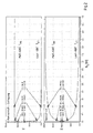
- FIG. 2 shows a relative static current imbalance for a given shunt resistor R S in an emitter path for the case of a load-carrying or load IGBT T L1 and a measurement IGBT T M1 .
- this shows the deviation from the nominal current or from the evenly distributed saturation current.
- FIG. 2 shows the current distribution between load IGBT T L1 and measurement IGBT T M1 .
- the upper half of the figure relates to a short-circuit condition, ie saturation, while the lower half of the figure illustrates the situation at nominal current, plotted against the size of the shunt resistance R S , which was chosen between 0.01 ⁇ and 10 ⁇ .
- the current imbalance becomes essential for shunt resistors R S above 1 ⁇ .
- this can also be used to break down the current for the shunt resistor R S , thereby reducing its power rating. It must of course be guaranteed that the shunt resistor R S still sees a proportional current that allows it to detect a short circuit.
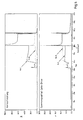
- FIG 3 shows in the top diagram a voltage difference across the shunt resistor R S for the nominal operation and for saturation.
- R S 1 ⁇
- the voltage across the shunt resistor R S for a short circuit is 2.6885V higher than in nominal operation. This would be sufficient for an entry.
- the two other graphs show the assumed peak power in the shunt resistor R S and the average power loss in the shunt resistor R S.
- FIG. 4 shows a power loss (upper curve) or a measured voltage drop in the gate drive (lower curve) for the shunt resistor R S in the event of a switch-on to 50% of the rated current and then a short circuit after 80 ⁇ s, in each case for two different shunt resistors R S of 1 ⁇ or 10 ⁇ .
- the use of a shunt resistor with an emitter follower is proposed.
- the voltage across the shunt resistor is relatively small and can easily be affected by noise. It is therefore very important to route the signal to a low resistance path.
- the first exemplary embodiment of the invention consists in an emitter follower integrated in a module, as shown in FIG. 5.
- the circuit is constructed as follows: The measurement IGBT T M1 is connected in parallel to a load-carrying or load IGBT T L1 .
- the two interconnections for the IGBT modules T M1 and T L1 are identical, with the difference that a sensor or a current measuring device 1 is additionally formed in the path in which the current measurement is carried out.
- a bit stream 2 is supplied to a gate electronics or a gate drive 3, which then generates a voltage output signal V AusM , V AusL , which is transmitted via a resistor R (for example 10 ⁇ ) is applied to the gate of the load IGBT T L1 .
- a free-wheeling diode D L1 is formed parallel to the load IGBT T L1 .
- a voltage source U 1 is formed, which outputs a voltage of 2800 V, for example.
- the voltage output signal V AusM or V AusL of the gate drive 3 is fed via a further resistor R (for example 10 ⁇ ) to a gate of a measurement IGBT T M1 , the emitter connection of which is connected to the load IGBT T L1 via a shunt resistor R S is.
- a base of a PNP transistor T 3 or T 4 is connected between the emitter and the shunt resistor R S , whose emitter is connected via a resistor R 2 (for example 100 k ⁇ ) to the positive output of a voltage source U 2 (for example 22.5 V ) is connected, while the collector is connected via a resistor R 1 (eg 1 k ⁇ ) both to the negative output of the voltage source U 2 and to the emitter of the load IGBT T L1 .
- the response voltage at the connection is advantageously always 0.7 V higher than the base voltage of the NPN transistor, so that negative effects of noise are reduced become. For this reason, a regular bipolar small signal transistor can be used as transistor T 3 or T 4 .
- a shunt resistor R S with a saturation transistor is used as the basic amplifier.
- This circuit is shown in Fig. 6.
- the measurement IGBT T M1 is connected in parallel to a load-carrying or load IGBT T L1 .
- the two interconnections for the IGBT modules T M1 and T L1 are identical, with the difference that a sensor or a current measuring device 1 is additionally formed in the path in which the current measurement is carried out.
- a bit stream 2 is fed to a gate electronics or a gate drive 3, which then generates a voltage output signal V AusM , V AusL , which is transmitted via a resistor R (for example 10 ⁇ ) is applied to the gate of the load IGBT T L1 .
- a free-wheeling diode D L1 is formed parallel to the load IGBT T L1 .
- a voltage source U 1 is formed, which outputs a voltage of 2800 V, for example.
- the voltage output signal V AusM or V AusL of the gate drive 3 is fed via a further resistor R (for example 10 ⁇ ) to a gate of a measurement IGBT T M1 , the emitter connection of which is connected to the emitter connection of the load IGBT T via a shunt resistor R S L1 is connected.
- a PNP transistor T 5 or T 6 is connected between the emitter and the shunt resistor R S , the base of which is connected to an emitter of the load IGBT T L and a positive output of a voltage source U 3 or U 4 (gate Drive supply voltage) is connected.
- these voltages can, however, be selected independently of the detection device described here in order to enable loss-optimized normal operation of the IGBTs.
- the shunt resistor voltage is amplified by a PNP transistor T 5 or T 6 , which is operated in a basic circuit.
- the circuit is designed such that the bipolar (small signal) transistor T 5 or T 6 is saturated whenever the load IGBT T L1 carries too much current. This gives a very sharp voltage response.
- the voltage response against the negative gate drive supply voltage must be measured.
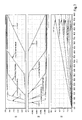
- FIG. 7 shows the static behavior of this shunt resistor arrangement with a saturating base amplifier according to FIG. 6.
- the top graph shows the response voltage at the output (collector) of the amplifier T 5 .
- the second graph shows the current flowing in the module, which actually flows out of the module towards the negative gate drive supply voltage U 3 .
- the bottom graph shows the voltage across the shunt resistor R S.
- the parameter is the total shunt resistance R S , the contribution of transistor T 5 not being taken into account.
- the upper graph shows the current distribution between load-bearing or load IGBT T L1 and measurement IGBT T M1 . It can be seen from this that at nominal current, that is to say under normal conditions, both IGBTs have approximately the same current as current, while in the case of saturation the measurement IGBT T M1 draws less current (shown in dashed lines in FIG. 8), with the worst case always here the use of only one load IGBT T L1 and one measurement IGBT T M1 is considered.
- the lower graph shows the measurement response, ie the voltage across a measurement resistor R 3 , this voltage being measured against the negative gate drive supply voltage U 3 of -7.5V. The response is essentially instantaneous and depends only on the level to which it was adjusted.
- the present invention discloses an overcurrent detector, with the overcurrents that lead to destruction of shutdown Semiconductor components could lead, measured quickly and reliably and thereby the destruction of the semiconductor device can be prevented without that total currents in the kA range must be measured. This is done in a Parallel connection of a measuring semiconductor component that can be switched off and at least a load-bearing semiconductor component that can be switched off in the current measurement path a current measuring device is formed. It is also anti-parallel to the switchable load-bearing semiconductor component formed a free-wheeling diode.
- Embodiments include the overcurrent detection device according to the invention either a shunt resistor with a saturation transistor as a basic amplifier or a shunt resistor with a Emitter follower.
- at least one load branch is parallel to the one that can be switched off load-bearing semiconductor component, the switchable measurement semiconductor component trained, with the emitter of a shunt resistor connected is.
- Between the emitter of the measuring semiconductor component that can be switched off and the shunt resistance is either the basis of one Bipolar transistor or the emitter of a bipolar transistor connected.
Landscapes
- Engineering & Computer Science (AREA)
- Power Engineering (AREA)
- Power Conversion In General (AREA)
- Electronic Switches (AREA)
- Measurement Of Current Or Voltage (AREA)
Abstract
Description
Claims (8)
- Überstromerfassungseinrichtung mit mindestens einem Schaltungszweig mit:wobei zwischen dem Emitter des abschaltbaren Mess-Halbleiterbauelements (TM1, TM2) und dem Nebenschlusswiderstand (RS) die Basis eines Transistors (T3, T4) angeschlossen ist, dessen Kollektor über einen dritten Widerstand (R1) mit einem negativen Anschluss einer Spannungsquelle (U2) und dem Emitter des abschaltbaren Last-Halbleiterbauelements (TL1, TL2) verbunden ist, während der Emitter über einen vierten Widerstand (R2) mit einem positiven Anschluss der Spannungsquelle (U2) verbunden ist.einem abschaltbaren Mess-Halbleiterbauelement (TM1, TM2) parallel zu mindestens einem abschaltbaren Last-Halbleiterbauelement (TL1, TL2),einer Strommesseinrichtung (1) im Pfad des abschaltbaren Mess-Halbleiterbauelements (TM1),sowohl im Pfad des abschaltbaren Mess-Halbleiterbauelements (TM1, TM2) als auch im mindestens einen Pfad des abschaltbaren Last-Halbleiterbauelements (TL1, TL2):einer gemeinsamen Einrichtung (2) zur Erzeugung eines Bitstroms, der einem gemeinsamen Gate-Drive (3) zugeführt wird, zur Ausgabe eines Spannungsausgangssignals (VAusM, VAusL) ansprechend auf den Bitstrom über einen ersten Widerstand (R) an das Gate des abschaltbaren Last-Halbleiterbauelements (TL1, TL2) und über einen zweiten Widerstand (R) an das Gate des abschaltbaren Mess-Halbleiterbauelements (TM1, TM2), dessen Emitteranschluss über einen Nebenschlusswiderstand (RS) mit dem Emitteranschluss des abschaltbaren Last-Halbleiterbauelements (TL1, TL2) verbunden ist,
- Überstrom-Erfassungseinrichtung nach Anspruch 1, wobei
der erste und der zweite Widerstand (R) jeweils einen Wert von 10Ω aufweisen, während der dritte Widerstand (R1) einen Wert von 1kΩ und der vierte Widerstand (R2) einen Wert von 100 kΩ aufweisen. - Überstrom-Erfassungseinrichtung, mit mindestens einem Schaltungszweig mit:wobei zwischen dem Emitter des abschaltbaren Mess-Halbleiterbauelements (TM1, TM2) und dem Nebenschlusswiderstand (RS) der Emitter eines Transistors (T5, T6) angeschlossen ist, dessen Kollektor über einen fünften Widerstand (R3) mit einem negativen Anschluss der Spannungsquelle (U3, U4) verbunden ist, während die Basis des Transistors (T5, T6) sowohl mit dem positiven Anschluss der Spannungsquelle (U3, U4) als auch mit dem Emitter des abschaltbaren Last-Halbleiterbauelements (TL1, TL2) verbunden ist.einem abschaltbaren Mess-Halbleiterbauelement (TM1, TM2) parallel zu mindestens einem abschaltbaren Last-Halbleiterbauelement (TL1, TL2),einer Strommesseinrichtung (1) im Pfad des abschaltbaren Mess-Halbleiterbauelements (TM1),sowohl im Pfad des abschaltbaren Mess-Halbleiterbauelements (TM1, TM2) als auch im mindestens einen Pfad des abschaltbaren Last-Halbleiterbauelements (TL1, TL2):einer gemeinsamen Einrichtung (2) zur Erzeugung eines Bitstroms, der einem gemeinsamen Gate-Drive (3) zugeführt wird, zur Ausgabe eines Spannungsausgangssignals (VAusM, VAusL) ansprechend auf den Bitstrom über einen ersten Widerstand (R) an das Gate des abschaltbaren Last-Halbleiterbauelements (TL1, TL2) und über einen zweiten Widerstand (R) an das Gate des abschaltbaren Mess-Halbleiterbauelements (TM1, TM2), dessen Emitteranschluss über einen Nebenschlusswiderstand (RS) sowohl mit einem positiven Anschluss einer Spannungsquelle (U3, U4) als auch mit dem Emitter des abschaltbaren Last-Halbleiterbauelementes (TL1, TL2) verbunden ist,
- Überstrom-Erfassungseinrichtung nach Anspruch 3, wobei
der erste und der zweite Widerstand (R) jeweils einen Wert von 10Ω aufweisen, während der fünfte Widerstand (R3) einen Wert von 1kΩ aufweist. - Überstrom-Erfassungseinrichtung nach einem der vorhergehenden Ansprüche 1 bis 4, wobei
der Nebenschlusswiderstand (RS) einen Wert im Bereich zwischen 0,01Ω und 10Ω aufweist. - Überstrom-Erfassungseinrichtung nach einem der vorhergehenden Ansprüche 1 bis 5, wobei
als abschaltbare Halbleiterbauelemente Bipolartransistoren (TL1, TM1, TL2, TM2) mit isoliert angeordneter Gate-Elektrode verwendet werden. - Überstrom-Erfassungseinrichtung nach einem der vorhergehenden Ansprüche 1 bis 6, wobei
als Transistoren (T3, T4; T5, T6) Bipolar-Kleinsignaltransistoren verwendet werden. - Überstrom-Erfassungseinrichtung nach Anspruch 7, wobei
die Transistoren (T3, T4; T5, T6) PNP-Transistoren sind.
Applications Claiming Priority (2)
| Application Number | Priority Date | Filing Date | Title |
|---|---|---|---|
| DE10060553 | 2000-12-06 | ||
| DE2000160553 DE10060553A1 (de) | 2000-12-06 | 2000-12-06 | Überstrom-Erfassungseinrichtung |
Publications (2)
| Publication Number | Publication Date |
|---|---|
| EP1213827A2 true EP1213827A2 (de) | 2002-06-12 |
| EP1213827A3 EP1213827A3 (de) | 2004-06-16 |
Family
ID=7665962
Family Applications (1)
| Application Number | Title | Priority Date | Filing Date |
|---|---|---|---|
| EP01250429A Withdrawn EP1213827A3 (de) | 2000-12-06 | 2001-12-06 | Überstrom-Erfassungseinrichtung |
Country Status (2)
| Country | Link |
|---|---|
| EP (1) | EP1213827A3 (de) |
| DE (1) | DE10060553A1 (de) |
Family Cites Families (4)
| Publication number | Priority date | Publication date | Assignee | Title |
|---|---|---|---|---|
| JPH0479758A (ja) * | 1990-07-19 | 1992-03-13 | Fuji Electric Co Ltd | 電流センスigbtの駆動回路 |
| JPH07146722A (ja) * | 1993-10-01 | 1995-06-06 | Fuji Electric Co Ltd | トランジスタ用過電流保護装置 |
| JP3414859B2 (ja) * | 1993-09-09 | 2003-06-09 | シーメンス アクチエンゲゼルシヤフト | 半導体デバイスの過電流時のターンオフ回路装置 |
| JPH11112313A (ja) * | 1997-10-02 | 1999-04-23 | Mitsubishi Electric Corp | 半導体回路及びパワートランジスタ保護回路 |
-
2000
- 2000-12-06 DE DE2000160553 patent/DE10060553A1/de not_active Withdrawn
-
2001
- 2001-12-06 EP EP01250429A patent/EP1213827A3/de not_active Withdrawn
Also Published As
| Publication number | Publication date |
|---|---|
| EP1213827A3 (de) | 2004-06-16 |
| DE10060553A1 (de) | 2002-06-13 |
Similar Documents
| Publication | Publication Date | Title |
|---|---|---|
| DE3685733T2 (de) | Stromdetektorschaltung fuer eine leistungshalbleitervorrichtung, insbesondere einen integrierten leistungshalbleiterschalter, speziell zur verwendung in motorfahrzeugen. | |
| DE19614354C2 (de) | Steuerschaltung für eine MOS-Gate-gesteuerte Leistungshalbleiterschaltung | |
| DE19533103B4 (de) | Schaltungsanordnung zum Betrieb einer Entladungslampe | |
| DE4207568C2 (de) | Überstrom-Detektorschaltung für eine Leistungshalbleiteranordnung | |
| DE3622268C1 (de) | Sicherheitsbarriere | |
| DE68925163T2 (de) | Treiberschaltung für Transistor mit isoliertem Gate; und deren Verwendung in einem Schalterkreis, einer Stromschalteinrichtung, und einem Induktionsmotorsystem | |
| DE2754409B2 (de) | Schaltungsanordnung zum Schützen von Fernsprechleitungen | |
| DE69500031T2 (de) | Steuerungsschaltung und Anordnung für eine Niederdruckleuchtstofflampe | |
| DE69112908T2 (de) | Verfahren und Vorrichtung zum Schutz von Thyristoren. | |
| DE2851461A1 (de) | Schaltverstaerker, schutzschaltung und verfahren zum schutz eines schalttransistors | |
| DE2646171A1 (de) | Stromstoss-schutzschaltung | |
| DE102012024728A1 (de) | Verfahren und Vorrichtung zur Überwachung einer elektrischen Anlage auf einen Rückstrom | |
| DE2263867A1 (de) | Steuerschaltung fuer thyristoren | |
| DE69614659T2 (de) | Schaltung mit Überstromschutz für Leistungstransistoren | |
| DE102006008292B4 (de) | Überlastschutz für steuerbare Stromverbraucher | |
| DE69220732T2 (de) | Schutz von Halbleitern vor Transienten hoher Energie | |
| DE2938344A1 (de) | Sicherheitsschaltung zur uebewachung von magnetventilen von fahrzeugen | |
| DE2814021A1 (de) | Transistorschalteinrichtung | |
| EP2132851A1 (de) | Schaltungsanordnung zur spannungsbegrenzung | |
| DE3402341C2 (de) | ||
| DE4142666C2 (de) | Schaltungsanordnung mit einem Halbleiterschalter zum Schalten einer Last | |
| AT404414B (de) | Thyristorschutz durch wechselrichterkipperkennung | |
| DE10060553A1 (de) | Überstrom-Erfassungseinrichtung | |
| DE10006526A1 (de) | Temperaturgeschützte Halbleiterschaltungsanordnung | |
| DE19546132C2 (de) | Schaltungsanordnung zum Schutz vor eingangsseitigem Überstrom bei Spannungszwischenkreisumrichtern |
Legal Events
| Date | Code | Title | Description |
|---|---|---|---|
| PUAI | Public reference made under article 153(3) epc to a published international application that has entered the european phase |
Free format text: ORIGINAL CODE: 0009012 |
|
| AK | Designated contracting states |
Kind code of ref document: A2 Designated state(s): AT BE CH CY DE DK ES FI FR GB GR IE IT LI LU MC NL PT SE TR |
|
| AX | Request for extension of the european patent |
Free format text: AL;LT;LV;MK;RO;SI |
|
| PUAL | Search report despatched |
Free format text: ORIGINAL CODE: 0009013 |
|
| AK | Designated contracting states |
Kind code of ref document: A3 Designated state(s): AT BE CH CY DE DK ES FI FR GB GR IE IT LI LU MC NL PT SE TR |
|
| AX | Request for extension of the european patent |
Extension state: AL LT LV MK RO SI |
|
| RIC1 | Information provided on ipc code assigned before grant |
Ipc: 7H 01L 27/02 B Ipc: 7H 03K 17/082 A |
|
| AKX | Designation fees paid | ||
| REG | Reference to a national code |
Ref country code: DE Ref legal event code: 8566 |
|
| STAA | Information on the status of an ep patent application or granted ep patent |
Free format text: STATUS: THE APPLICATION IS DEEMED TO BE WITHDRAWN |
|
| 18D | Application deemed to be withdrawn |
Effective date: 20041217 |