EP1212583B1 - Einrichtung zur inspektion einer dreidimensionalen oberflächenstruktur - Google Patents
Einrichtung zur inspektion einer dreidimensionalen oberflächenstruktur Download PDFInfo
- Publication number
- EP1212583B1 EP1212583B1 EP00962234A EP00962234A EP1212583B1 EP 1212583 B1 EP1212583 B1 EP 1212583B1 EP 00962234 A EP00962234 A EP 00962234A EP 00962234 A EP00962234 A EP 00962234A EP 1212583 B1 EP1212583 B1 EP 1212583B1
- Authority
- EP
- European Patent Office
- Prior art keywords
- values
- tolerance range
- surface structure
- solder paste
- inspected
- Prior art date
- Legal status (The legal status is an assumption and is not a legal conclusion. Google has not performed a legal analysis and makes no representation as to the accuracy of the status listed.)
- Expired - Lifetime
Links
Images
Classifications
-
- G—PHYSICS
- G01—MEASURING; TESTING
- G01N—INVESTIGATING OR ANALYSING MATERIALS BY DETERMINING THEIR CHEMICAL OR PHYSICAL PROPERTIES
- G01N21/00—Investigating or analysing materials by the use of optical means, i.e. using sub-millimetre waves, infrared, visible or ultraviolet light
-
- G—PHYSICS
- G01—MEASURING; TESTING
- G01B—MEASURING LENGTH, THICKNESS OR SIMILAR LINEAR DIMENSIONS; MEASURING ANGLES; MEASURING AREAS; MEASURING IRREGULARITIES OF SURFACES OR CONTOURS
- G01B11/00—Measuring arrangements characterised by the use of optical techniques
- G01B11/24—Measuring arrangements characterised by the use of optical techniques for measuring contours or curvatures
-
- G—PHYSICS
- G01—MEASURING; TESTING
- G01B—MEASURING LENGTH, THICKNESS OR SIMILAR LINEAR DIMENSIONS; MEASURING ANGLES; MEASURING AREAS; MEASURING IRREGULARITIES OF SURFACES OR CONTOURS
- G01B11/00—Measuring arrangements characterised by the use of optical techniques
- G01B11/30—Measuring arrangements characterised by the use of optical techniques for measuring roughness or irregularity of surfaces
- G01B11/306—Measuring arrangements characterised by the use of optical techniques for measuring roughness or irregularity of surfaces for measuring evenness
-
- G—PHYSICS
- G01—MEASURING; TESTING
- G01N—INVESTIGATING OR ANALYSING MATERIALS BY DETERMINING THEIR CHEMICAL OR PHYSICAL PROPERTIES
- G01N21/00—Investigating or analysing materials by the use of optical means, i.e. using sub-millimetre waves, infrared, visible or ultraviolet light
- G01N21/84—Systems specially adapted for particular applications
- G01N21/88—Investigating the presence of flaws or contamination
-
- H—ELECTRICITY
- H05—ELECTRIC TECHNIQUES NOT OTHERWISE PROVIDED FOR
- H05K—PRINTED CIRCUITS; CASINGS OR CONSTRUCTIONAL DETAILS OF ELECTRIC APPARATUS; MANUFACTURE OF ASSEMBLAGES OF ELECTRICAL COMPONENTS
- H05K13/00—Apparatus or processes specially adapted for manufacturing or adjusting assemblages of electric components
- H05K13/08—Monitoring manufacture of assemblages
- H05K13/081—Integration of optical monitoring devices in assembly lines; Processes using optical monitoring devices specially adapted for controlling devices or machines in assembly lines
- H05K13/0817—Monitoring of soldering processes
-
- H—ELECTRICITY
- H05—ELECTRIC TECHNIQUES NOT OTHERWISE PROVIDED FOR
- H05K—PRINTED CIRCUITS; CASINGS OR CONSTRUCTIONAL DETAILS OF ELECTRIC APPARATUS; MANUFACTURE OF ASSEMBLAGES OF ELECTRICAL COMPONENTS
- H05K3/00—Apparatus or processes for manufacturing printed circuits
- H05K3/30—Assembling printed circuits with electric components, e.g. with resistors
- H05K3/32—Assembling printed circuits with electric components, e.g. with resistors electrically connecting electric components or wires to printed circuits
- H05K3/34—Assembling printed circuits with electric components, e.g. with resistors electrically connecting electric components or wires to printed circuits by soldering
- H05K3/3465—Application of solder
- H05K3/3485—Application of solder paste, slurry or powder
Definitions
- the invention relates to a device for inspecting a three-dimensional surface structure according to the generic term of claim 1.
- Such a device for inspecting a three-dimensional Surface structure is already out of the DE 196 08 468 C2 known. It is suitable for inspection a three-dimensional surface structure essentially one level specimen, especially for inspection of solder paste printing on circuit boards. With an optical sensor a part of the surface of the test object becomes three-dimensional detected. A positioning device is used for relative positioning of the optical sensor to the test object, thus different parts of the surface one after the other can be inspected.
- the inspection can be used to advantage of solder paste printing on printed circuit boards.
- constant monitoring of the solder paste pressure is required. Errors caused by screen printing can so before assembling the circuit board with components recognized and faulty circuit boards even before they are created additional costs can be eliminated.
- Printed circuit boards for surface mountable Components so-called circuit boards in Surface mount technology (SMT) are used in large quantities and produced many variants. The surface mountable Components are soldered onto the circuit board Connections on metallized surfaces, so-called pads, mechanically held and electrically with conductor tracks on the PCB connected.
- Patterns of metallic pads are provided to help position the Connections of the component correspond.
- solder paste is applied to the pads. After that the surface-mountable component is on the circuit board stocked. First, the component is through the Adhesive property of the solder paste kept on the circuit board. After heating the assembled printed circuit board the connections of the component with the pads are fixed soldered.
- Fine pitch range is the distance between two adjacent Connections of a component about 0.0635 cm (1/40 inch). This also applies to the pads on the circuit boards smaller and denser. About 80% of soldering errors are in the fine pitch range caused by the solder paste printing. Examples solder paste application is too low for such errors or short circuits between adjacent pads due to inaccurate Placement of the screen printing stencil during solder paste printing. Around to find these defects and weak points in the manufacturing process an optical inspection after the solder paste application made of the circuit board.
- the invention has for its object a device for the inspection of a three-dimensional surface structure create, in which the setting of the limit values, on compliance with measured values of geometric properties an inspected surface structure are checked for the operator is simplified.
- the invention has the advantage that the limit values are defined requires considerably less time and thus an inspection of the solder paste printing on printed circuit boards causes lower costs.
- the calculation of the limit values geometric properties of the solder paste application through a program in the control computer of the inspection facility can be integrated. The user does not have to do more manual calculations.
- the invention is particularly useful when testing the solder paste application can advantageously be used on a printed circuit board because to test many different geometric properties here and thus many different limit values have to be calculated.
- Tracking the test program sequence is advantageous and the results of the individual test steps for the Operator allows if means to output the measured Values of the geometric properties of an inspected Surface structure available on the inspection facility are.
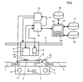
- An inspection facility the basic structure of which is in The figure shown can be used in a printed circuit board production line be incorporated.
- the untested circuit boards the inspection facility with a conveyor belt 1 fed.
- a tiltable stopper 2 With a tiltable stopper 2, the hidden parts are drawn with broken lines, is a circuit board 3 to be inspected in each case Inspection position held. After the inspection is completed the stopper 2 sunk down and the circuit board 3 is with a conveyor belt 4 from the inspection device out and with a conveyor belt 5 to further, in the Drawing not shown processing stations transported.
- circuit boards are usually used summarized a benefit and together with a means of transport moved in the production line.
- the better clarity is due to the illustration in the figure a means of transport with a printed circuit board benefit Service.
- the axes of the machine coordinates of the inspection device are indicated by arrows X and Y.
- the arrow Y stands at right angles to the arrow X and points vertically into the Drawing level.
- a sensor unit 6 in which an optical sensor 7, the is designed as a confocal microscope, and a CCD camera 8 are summarized. So that the sensor unit 6 over any Set the circuit board 3 for inspection of the Inspectable features can be positioned, they can be positioned on a guide axis 9 can be moved in the X direction.
- the Printed circuit board holder is arranged on a carriage 12 which mounted on two axes 10 and 11 movable in the Y direction is.
- the upper circular area of the calibration mark 16 is blackened for a better contrast of the gray values.
- the optical sensor 7th and the CCD camera 8 exactly after calibration the features to be inspected and the geometric Measure the dimensions and the location of the features become.
- a surface structure to be inspected is a solder deposit 19 on the printed circuit board 3 shown that on a metallic solder pad 20 when applying solder paste has been applied.
- a computing unit 29 the one with an on-screen display 33 and an input keyboard 34 is provided, serves to operate the inspection device during calibration, during fine adjustment as well as during the actual inspection process. On the Screen display 33 can states of the inspection device as well as inspection results are displayed and with the input keyboard 34 required operator inputs have been made become.
- Setpoints for geometrical values are stored in a first memory 30 Properties of the surface structure to be inspected filed. This is the case in this exemplary embodiment among other things, data from the pads, for example the pad 20, by means of a CAD converter from the CAD data of the circuit board 3 can be won. Because the thickness of the for Solder paste application usually used screen printing stencil cannot be extracted from CAD data, Operator entered as parameters via the input keyboard 34. Likewise, any necessary reduction factors entered for the template openings. additionally is used for the parameterization of the image processing algorithms an indication of the thickness of the solder mask is required. Based This information can be used, for example, by an edge search algorithm between an edge of a pad and an edge of the Differentiate solder resists. Using the pad data and the Manually entered values become the theoretical parameters for area, height, volume and coverage of the solder paste application calculated on the pads as target values.
- a second memory 31 there are values for specifying the Relative tolerance range for the geometric properties stored. These values are individual theoretical Assigned parameters. From the setpoints in the memory 30 and the values of the relative tolerance ranges in the memory 31 the computing unit calculates 29 limit values of absolute tolerance ranges, which are stored in a third memory 32 become.
- the memories 30, 31 and 32 are for better clarity shown separately. You can take it for granted in practice are on the same storage medium.
- a mask is output, the input fields for the template thickness in micrometers, the thickness of the solder resist in micrometers, a reduction factor of Stencil breakthroughs in the X direction, a reduction factor the stencil openings in the Y direction, a center offset the perforations in the X direction in the unit Micrometers and a center offset of the stencil openings contains micrometers in the Y direction in the unit.
- the manually entered template data are used for the calculation the theoretical parameters of the solder paste application used.
- An auxiliary variable used here is the pad area, which is, for example, a rectangular pad as the product of pad width and pad length.
- the area of the Solder paste application on a pad is calculated as the product from pad width, reduction factor in Y direction, pad length and reduction factor in the X direction.
- the volume of the Solder paste application is calculated as the product of the area and the template thickness.
- An absolute offset of the solder paste application in the X direction is equal to the amount entered Center offset of the template openings in the X direction absolute offset in the Y direction corresponds to the entered Amount of the center offset in the Y direction.
- a relative offset in the X direction calculated, which is the quotient of the amount entered the center offset in the X direction and the pad length.
- a relative offset in the Y direction is the quotient of the entered amount of the center offset in the Y direction and the Pad width calculated.
- a degree of coverage of the pad is called Quotient from the area of the solder paste application and the pad area calculated.
- An upper limit for the absolute Offset in the X direction is the sum of the setpoint of the absolute offset in the X direction and the product of the Pad length and a relative tolerance value of the offset calculated. Accordingly, an upper limit for the absolute Offset in the Y direction as the sum of the setpoint of the absolute offset in the Y direction and the product of the pad width and a relative tolerance value of the offset.
- An upper and a lower limit of the degree of coverage is determined from the target value of the degree of coverage and the assigned relative tolerance ranges.
- the circuit board 3 must - as described above - theoretically calculated limit values of the absolute tolerance ranges, that have been stored in memory 32 for inspection of the solder paste application can still be fine-tuned.
- the individual surface structures to be inspected approached and measured.
- an operator can press a "Show errors" button cause the measured Values of the geometric properties and the recorded Height image and the gray value image of the solder paste application on the screen display 33 are shown.
- the measured Values representing the limit values of the absolute tolerance range are shown with a red color highlighted against the otherwise green values, so that the operator's attention directly on these values is drawn. Based on the displayed measured Values and images allow the operator to decide whether it is the detected error is a pseudo error or a actual error.
- An error is called a pseudo error referred to when the measured values of the geometric Property outside the limits of the absolute Tolerance range, but due to the spread of the manufacturing process must nevertheless be described as good.
Landscapes
- Physics & Mathematics (AREA)
- General Physics & Mathematics (AREA)
- Engineering & Computer Science (AREA)
- Biochemistry (AREA)
- Immunology (AREA)
- Microelectronics & Electronic Packaging (AREA)
- Health & Medical Sciences (AREA)
- Life Sciences & Earth Sciences (AREA)
- Chemical & Material Sciences (AREA)
- Analytical Chemistry (AREA)
- Operations Research (AREA)
- General Health & Medical Sciences (AREA)
- Manufacturing & Machinery (AREA)
- Pathology (AREA)
- Investigating Materials By The Use Of Optical Means Adapted For Particular Applications (AREA)
- Electric Connection Of Electric Components To Printed Circuits (AREA)
- Length Measuring Devices By Optical Means (AREA)
- Length Measuring Devices With Unspecified Measuring Means (AREA)
- Analysing Materials By The Use Of Radiation (AREA)
- Image Input (AREA)
Description
Claims (6)
- Einrichtung zur Inspektion einer dreidimensionalen Oberflächenstruktur eines im wesentlichen ebenen Prüflings, insbesondere zur Inspektion des Lotpastendrucks auf Leiterplatten,dadurch gekennzeichnet,mit einem optischen Sensor (7) zur dreidimensionalen Erfassung zumindest eines Teilbereichs der Oberfläche des Prüflings (3) undmit einer Positioniereinrichtung (9 ... 13), mit welcher der optische Sensor (7) und der Prüfling (3) relativ zueinander positionierbar sind,daß in einem ersten Speicher (30) Sollwerte für geometrische Eigenschaften der zu inspizierenden Oberflächenstruktur abgelegt sind,daß in einem zweiten Speicher (31) Werte zur Angabe des relativen Toleranzbereichs für die geometrischen Eigenschaften abgelegt sind,daß eine Recheneinheit (29) vorhanden ist zur Berechnung von Grenzwerten eines absoluten Toleranzbereichs unddaß Mittel zur Anzeige eines Fehlers vorhanden sind, wenn ein gemessener Wert einer geometrischen Eigenschaft einer inspizierten Oberflächenstruktur nicht innerhalb ihres absoluten Toleranzbereichs liegt.
- Einrichtung nach Anspruch 1, dadurch gekennzeichnet,daß die zu inspizierende Oberflächenstruktur ein Lotpastenauftrag (19) auf einer Anschlußfläche (20), einem sogenannten Pad, für einen Bauelementeanschluß auf einer Leiterplatte (3) ist unddaß die geometrischen Eigenschaften die Fläche, die Höhe, das Volumen des Lotpastenauftrags (19) und/oder der Versatz des Lotpastenauftrags (19) gegenüber dem Pad (20) sind.
- Einrichtung nach Anspruch 1 oder 2, dadurch gekennzeichnet,daß Mittel (33) zur Ausgabe der gemessenen Werte der geometrischen Eigenschaften einer inspizierten Oberflächenstruktur vorhanden sind.
- Einrichtung nach Anspruch 3, dadurch gekennzeichnet,daß ein Ausgabemittel (33) ein Bildschirm ist, auf welchem gemessene Werte einer geometrischen Eigenschaft, die außerhalb ihres absoluten Toleranzbereichs liegen, durch die Art der Darstellung, insbesondere durch die Farbe, gegenüber gemessenen Werten anderer geometrischer Eigenschaften, die innerhalb ihres absoluten Toleranzbereichs liegen, hervorgehoben sind.
- Einrichtung nach Anspruch 3 oder 4, dadurch gekennzeichnet,daß ein Eingabemittel (34) vorgesehen ist, mit welchem von einem Bediener vorgebbar ist, ob ein gemessener Wert einer geometrischen Eigenschaft, der außerhalb des absoluten Toleranzbereichs liegt, als Fehler bewertet werden soll oder nicht, unddaß die Recheneinheit (29) derart ausgestaltet ist, daß im Falle einer Bewertung als kein Fehler der absolute Toleranzbereich der Werte der geometrischen Eigenschaft entsprechend dem gemessenen Wert angepaßt wird.
- Einrichtung nach einem der vorhergehenden Ansprüche,
dadurch gekennzeichnet,daß der optische Sensor (7) ein Höhenbild der zu inspizierenden Oberflächenstruktur aufnimmt unddaß auf der Bildschirmanzeige (33) das Höhenbild und/oder ein Grauwertbild darstellbar ist.
Applications Claiming Priority (3)
| Application Number | Priority Date | Filing Date | Title |
|---|---|---|---|
| DE29916075U DE29916075U1 (de) | 1999-09-13 | 1999-09-13 | Einrichtung zur Inspektion einer dreidimensionalen Oberflächenstruktur |
| DE29916075U | 1999-09-13 | ||
| PCT/DE2000/002855 WO2001020255A1 (de) | 1999-09-13 | 2000-08-22 | Einrichtung zur inspektion einer dreidimensionalen oberflächenstruktur |
Publications (2)
| Publication Number | Publication Date |
|---|---|
| EP1212583A1 EP1212583A1 (de) | 2002-06-12 |
| EP1212583B1 true EP1212583B1 (de) | 2003-05-28 |
Family
ID=8078839
Family Applications (1)
| Application Number | Title | Priority Date | Filing Date |
|---|---|---|---|
| EP00962234A Expired - Lifetime EP1212583B1 (de) | 1999-09-13 | 2000-08-22 | Einrichtung zur inspektion einer dreidimensionalen oberflächenstruktur |
Country Status (6)
| Country | Link |
|---|---|
| US (1) | US6710867B2 (de) |
| EP (1) | EP1212583B1 (de) |
| JP (1) | JP2003509668A (de) |
| AT (1) | ATE241798T1 (de) |
| DE (2) | DE29916075U1 (de) |
| WO (1) | WO2001020255A1 (de) |
Cited By (1)
| Publication number | Priority date | Publication date | Assignee | Title |
|---|---|---|---|---|
| DE102008041135A1 (de) * | 2008-08-08 | 2010-02-11 | Nanophotonics Ag | Inspektionsvorrichtung- und Verfahren für die optische Untersuchung von Objektoberflächen, insbesondere einer Wafernotch |
Families Citing this family (21)
| Publication number | Priority date | Publication date | Assignee | Title |
|---|---|---|---|---|
| JP3656543B2 (ja) * | 2000-10-25 | 2005-06-08 | 松下電器産業株式会社 | 電子部品実装方法 |
| US7324664B1 (en) * | 2003-10-28 | 2008-01-29 | Hewlett-Packard Development Company, L.P. | Method of and system for determining angular orientation of an object |
| JP3893132B2 (ja) * | 2004-01-22 | 2007-03-14 | アンリツ株式会社 | 印刷はんだ検査装置 |
| JP4997740B2 (ja) * | 2005-11-02 | 2012-08-08 | オムロン株式会社 | 生産管理装置、生産管理方法、生産管理システム、生産管理プログラム、および記録媒体 |
| US7545512B2 (en) * | 2006-01-26 | 2009-06-09 | Koh Young Technology Inc. | Method for automated measurement of three-dimensional shape of circuit boards |
| DE102008014742A1 (de) * | 2008-03-18 | 2009-09-24 | Qimonda Ag | Anordnung in Flip-Chip-Montagebauweise, Überprüfungsanordnung zum Überprüfen der Positionierung eines integrierten Schaltkreises relativ zu einem Träger einer Anordnung in Flip-Chip-Montagebauweise und Verfahren zum Überprüfen der Positionierung eines integrierten Schaltkreises relativ zu einem Träger einer Anordnung in Flip-Chip-Montagebauweise |
| JP6005359B2 (ja) * | 2008-08-28 | 2016-10-12 | コーニンクレッカ フィリップス エヌ ヴェKoninklijke Philips N.V. | 対象のサイズの変更を決定する装置 |
| JP5806454B2 (ja) * | 2010-08-25 | 2015-11-10 | アスリートFa株式会社 | オフコンタクト印刷方法、オフコンタクト印刷方法を用いた印刷装置及びオフコンタクト印刷方法を用いたボール搭載装置 |
| EP2764327B1 (de) * | 2011-11-14 | 2017-01-18 | Ev Group E. Thallner GmbH | Ermittlung von formänderungen eines substrats |
| CN107087388B (zh) | 2012-11-06 | 2020-02-28 | 株式会社高永科技 | 基板检查装置系统及基板检查方法 |
| LT2840874T (lt) * | 2013-08-19 | 2019-10-25 | Asm Assembly Sys Gmbh & Co Kg | Spausdinimo parametrų reguliavimas priklausomai nuo išmatuotų lituojamosios pastos liekanų tam tikrose spausdintinės plokštės zonose |
| CN104567664A (zh) * | 2013-10-29 | 2015-04-29 | 鸿富锦精密工业(深圳)有限公司 | 影像量测系统、影像量测系统的使用方法和终端装置 |
| JP2015161680A (ja) * | 2014-02-28 | 2015-09-07 | 株式会社キーエンス | 検査システム、画像処理装置、方法およびプログラム |
| US10081515B2 (en) * | 2014-06-09 | 2018-09-25 | Mitsubishi Electric Corporation | Method for measuring shaft and interference determination system |
| JP2016186982A (ja) * | 2015-03-27 | 2016-10-27 | 日本電気株式会社 | はんだ検査装置およびはんだ検査方法 |
| CN105334223B (zh) * | 2015-11-14 | 2017-11-28 | 苏州光韵达光电科技有限公司 | 一种全自动smt模板及检测系统 |
| CN105334232A (zh) * | 2015-11-20 | 2016-02-17 | 苏州光韵达光电科技有限公司 | 一种可移动的激光模板检测装置 |
| CN105572148A (zh) * | 2015-12-14 | 2016-05-11 | 天津华迈科技有限公司 | 一种贴片质检组件 |
| US11125697B2 (en) * | 2017-05-12 | 2021-09-21 | Fuji Corporation | Transfer state inspection system and component mounter |
| CN109657718B (zh) * | 2018-12-19 | 2023-02-07 | 广东省智能机器人研究院 | 一种数据驱动的smt生产线上spi缺陷类别智能识别方法 |
| CN111899248B (zh) * | 2020-08-05 | 2024-02-02 | 佛山市南海区广工大数控装备协同创新研究院 | 一种基于机器学习的自动pcb焊锡膏缺陷检测方法 |
Family Cites Families (11)
| Publication number | Priority date | Publication date | Assignee | Title |
|---|---|---|---|---|
| US3824387A (en) * | 1972-01-03 | 1974-07-16 | Owens Corning Fiberglass Corp | Method and apparatus for control of conditions in a process |
| US3902811A (en) * | 1973-06-27 | 1975-09-02 | Vsi Corp | Electro-optical scanning system for dimensional gauging of parts |
| DE59008567D1 (de) * | 1989-06-19 | 1995-04-06 | Maier Kg Andreas | Verfahren und Einrichtung zum Messen der Konturen eines Körpers. |
| JPH0794972B2 (ja) * | 1989-12-13 | 1995-10-11 | 松下電器産業株式会社 | 半田の外観検査方法 |
| US5619587A (en) * | 1991-05-10 | 1997-04-08 | Aluminum Company Of America | System and method for contactlessly gauging the thickness of a contoured object, such as a vehicle wheel |
| DE4410603C1 (de) * | 1994-03-26 | 1995-06-14 | Jenoptik Technologie Gmbh | Verfahren zur Erkennung von Fehlern bei der Inspektion von strukturierten Oberflächen |
| DE19608468C2 (de) * | 1996-03-01 | 1998-01-22 | Siemens Ag | Optischer Abstandssensor |
| US6175415B1 (en) * | 1997-02-19 | 2001-01-16 | United Technologies Corporation | Optical profile sensor |
| DE19713521B4 (de) * | 1997-04-02 | 2004-09-23 | Festo Ag & Co | Vorrichtung zur Erkennung falsch orientierter und/oder von einem vorgegebenen Muster abweichender Teile |
| US6181474B1 (en) * | 1999-03-22 | 2001-01-30 | Kovex Corporation | Scanning confocal microscope with objective lens position tracking |
| DE19915052A1 (de) | 1999-04-01 | 2000-10-05 | Siemens Ag | Einrichtung zur Inspektion einer dreidimensionalen Oberflächenstruktur sowie Verfahren zur Kalibrierung einer derartigen Einrichtung |
-
1999
- 1999-09-13 DE DE29916075U patent/DE29916075U1/de not_active Expired - Lifetime
-
2000
- 2000-08-22 EP EP00962234A patent/EP1212583B1/de not_active Expired - Lifetime
- 2000-08-22 WO PCT/DE2000/002855 patent/WO2001020255A1/de not_active Ceased
- 2000-08-22 AT AT00962234T patent/ATE241798T1/de not_active IP Right Cessation
- 2000-08-22 DE DE50002385T patent/DE50002385D1/de not_active Expired - Lifetime
- 2000-08-22 JP JP2001523594A patent/JP2003509668A/ja not_active Abandoned
-
2002
- 2002-03-12 US US10/095,005 patent/US6710867B2/en not_active Expired - Fee Related
Cited By (3)
| Publication number | Priority date | Publication date | Assignee | Title |
|---|---|---|---|---|
| DE102008041135A1 (de) * | 2008-08-08 | 2010-02-11 | Nanophotonics Ag | Inspektionsvorrichtung- und Verfahren für die optische Untersuchung von Objektoberflächen, insbesondere einer Wafernotch |
| WO2010015696A1 (de) * | 2008-08-08 | 2010-02-11 | Nanophotonics Ag | Inspektionsvorrichtung- und verfahren für die optische untersuchung von objektoberflächen, insbesondere einer wafernotch |
| DE102008041135B4 (de) * | 2008-08-08 | 2011-08-25 | NanoPhotonics AG, 55129 | Inspektionsvorrichtung- und Verfahren für die optische Untersuchung von Objektoberflächen, insbesondere einer Wafernotch |
Also Published As
| Publication number | Publication date |
|---|---|
| EP1212583A1 (de) | 2002-06-12 |
| WO2001020255A1 (de) | 2001-03-22 |
| DE50002385D1 (de) | 2003-07-03 |
| US20020180962A1 (en) | 2002-12-05 |
| ATE241798T1 (de) | 2003-06-15 |
| US6710867B2 (en) | 2004-03-23 |
| JP2003509668A (ja) | 2003-03-11 |
| DE29916075U1 (de) | 2000-12-14 |
Similar Documents
| Publication | Publication Date | Title |
|---|---|---|
| DE29916075U1 (de) | Einrichtung zur Inspektion einer dreidimensionalen Oberflächenstruktur | |
| DE69711043T2 (de) | Vorrichtung und verfahren zum siebdrucken | |
| DE112011104725B4 (de) | Lötstelleninspektionsverfahren, Leiterplatteninspektionssystem und Lötstelleninspektionsgerät | |
| DE112017007435B4 (de) | Komponentenbestückungssystem und klebemitteluntersuchungsvorrichtung | |
| DE4222804A1 (de) | Einrichtung und verfahren zur automatischen visuellen pruefung elektrischer und elektronischer baueinheiten | |
| DE102016125642A1 (de) | Prüfung und/oder Justierung einer Kamera, insbesondere einer digitalen Kamera, mittels eines optischen Prüfnormals | |
| DE4201943A1 (de) | Verfahren und vorrichtung zum pruefen einer verbindung eines elektronischen bauelements | |
| DE112006003089T5 (de) | System und Verfahren zum Montieren von elektronischen Bauelementen | |
| WO2001091053A1 (de) | Verfahren zum untersuchen einer leiterplatte an einem vorbestimmten bereich der leiterplatte und vorrichtung zum durchführen des verfahrens | |
| WO2018077356A1 (de) | Referenzplatte und verfahren zur kalibrierung und/oder überprüfung eines deflektometrie-sensorsystems | |
| DE102015201382A1 (de) | Qualitätssicherungssystem und Vorrichtung zur Innenprüfung | |
| DE102020105185B4 (de) | Datenkorrelation zwischen verschiedenen Maschinen einer Fertigungslinie für elektronische Bauelemente | |
| DE102014225987A1 (de) | Steuervorrichtung für eine Innenprüfungsvorrichtung und Verfahren zum Steuern einer Innenprüfungsvorrichtung | |
| DE19711476A1 (de) | Verfahren und Vorrichtung zum Vermessen einer Einrichtung zur Herstellung von elektrischen Baugruppen | |
| DE29823250U1 (de) | Schaltungsanordnung zur Prüfung von Lötstellen | |
| DE102004063488A1 (de) | Anlage zur automatischen Erkennung und Behebung von Lötfehlern an mit elektronischen Bauteilen bestückten Leiterplatten | |
| DE3540100A1 (de) | Verfahren zur optischen pruefung von leiterplatten | |
| WO1997017605A1 (de) | Verfahren und schaltungsanordnung zur prüfung von lötstellen | |
| EP0355377A1 (de) | Verfahren zur optischen Prüfung von Flachbaugruppen | |
| EP2661070B1 (de) | Verfahren und Vorrichtung zur Farbmessung an einem Druckbild | |
| DE10214817B4 (de) | Anordnung zur Höhenmessung des Lotpastenauftrages | |
| DE102016116201B4 (de) | Verfahren zum Auftragen von Pastenmaterial auf ein Substrat und zum ergänzenden Auftragen von Pastenmaterial auf ein Pastendepot des Substrats, Steuergerät, Computerprogrammprodukt und Siebdrucker | |
| DE19915052A1 (de) | Einrichtung zur Inspektion einer dreidimensionalen Oberflächenstruktur sowie Verfahren zur Kalibrierung einer derartigen Einrichtung | |
| DE4027902C2 (de) | Verfahren zur visuellen Prüfung bestückter Flachbaugruppen und Anordnung zur Durchführung des Verfahrens | |
| WO2001088473A1 (de) | Inspektion einer dreidimensionalen oberflächenstruktur sowie kalibrierung der auflösung (lotpastenauftrag) mit kamera und optischem sensor sowie unabhängiger kalibriermarke |
Legal Events
| Date | Code | Title | Description |
|---|---|---|---|
| PUAI | Public reference made under article 153(3) epc to a published international application that has entered the european phase |
Free format text: ORIGINAL CODE: 0009012 |
|
| 17P | Request for examination filed |
Effective date: 20020313 |
|
| AK | Designated contracting states |
Kind code of ref document: A1 Designated state(s): AT BE CH CY DE DK ES FI FR GB GR IE IT LI LU MC NL PT SE |
|
| AX | Request for extension of the european patent |
Free format text: AL;LT;LV;MK;RO;SI |
|
| R17P | Request for examination filed (corrected) |
Effective date: 20020121 |
|
| GRAH | Despatch of communication of intention to grant a patent |
Free format text: ORIGINAL CODE: EPIDOS IGRA |
|
| GRAH | Despatch of communication of intention to grant a patent |
Free format text: ORIGINAL CODE: EPIDOS IGRA |
|
| GRAA | (expected) grant |
Free format text: ORIGINAL CODE: 0009210 |
|
| AK | Designated contracting states |
Designated state(s): AT BE CH CY DE DK ES FI FR GB GR IE IT LI LU MC NL PT SE |
|
| PG25 | Lapsed in a contracting state [announced via postgrant information from national office to epo] |
Ref country code: IE Free format text: LAPSE BECAUSE OF FAILURE TO SUBMIT A TRANSLATION OF THE DESCRIPTION OR TO PAY THE FEE WITHIN THE PRESCRIBED TIME-LIMIT Effective date: 20030528 Ref country code: FI Free format text: LAPSE BECAUSE OF FAILURE TO SUBMIT A TRANSLATION OF THE DESCRIPTION OR TO PAY THE FEE WITHIN THE PRESCRIBED TIME-LIMIT Effective date: 20030528 |
|
| REG | Reference to a national code |
Ref country code: GB Ref legal event code: FG4D Free format text: NOT ENGLISH |
|
| REG | Reference to a national code |
Ref country code: CH Ref legal event code: EP |
|
| REG | Reference to a national code |
Ref country code: IE Ref legal event code: FG4D Free format text: GERMAN |
|
| REF | Corresponds to: |
Ref document number: 50002385 Country of ref document: DE Date of ref document: 20030703 Kind code of ref document: P |
|
| REG | Reference to a national code |
Ref country code: CH Ref legal event code: NV Representative=s name: SERVOPATENT GMBH |
|
| PG25 | Lapsed in a contracting state [announced via postgrant information from national office to epo] |
Ref country code: AT Free format text: LAPSE BECAUSE OF NON-PAYMENT OF DUE FEES Effective date: 20030822 Ref country code: LU Free format text: LAPSE BECAUSE OF NON-PAYMENT OF DUE FEES Effective date: 20030822 Ref country code: CY Free format text: LAPSE BECAUSE OF FAILURE TO SUBMIT A TRANSLATION OF THE DESCRIPTION OR TO PAY THE FEE WITHIN THE PRESCRIBED TIME-LIMIT Effective date: 20030822 |
|
| PG25 | Lapsed in a contracting state [announced via postgrant information from national office to epo] |
Ref country code: DK Free format text: LAPSE BECAUSE OF FAILURE TO SUBMIT A TRANSLATION OF THE DESCRIPTION OR TO PAY THE FEE WITHIN THE PRESCRIBED TIME-LIMIT Effective date: 20030828 Ref country code: SE Free format text: LAPSE BECAUSE OF FAILURE TO SUBMIT A TRANSLATION OF THE DESCRIPTION OR TO PAY THE FEE WITHIN THE PRESCRIBED TIME-LIMIT Effective date: 20030828 Ref country code: PT Free format text: LAPSE BECAUSE OF FAILURE TO SUBMIT A TRANSLATION OF THE DESCRIPTION OR TO PAY THE FEE WITHIN THE PRESCRIBED TIME-LIMIT Effective date: 20030828 Ref country code: GR Free format text: LAPSE BECAUSE OF FAILURE TO SUBMIT A TRANSLATION OF THE DESCRIPTION OR TO PAY THE FEE WITHIN THE PRESCRIBED TIME-LIMIT Effective date: 20030828 |
|
| PG25 | Lapsed in a contracting state [announced via postgrant information from national office to epo] |
Ref country code: MC Free format text: LAPSE BECAUSE OF NON-PAYMENT OF DUE FEES Effective date: 20030831 |
|
| PG25 | Lapsed in a contracting state [announced via postgrant information from national office to epo] |
Ref country code: ES Free format text: LAPSE BECAUSE OF FAILURE TO SUBMIT A TRANSLATION OF THE DESCRIPTION OR TO PAY THE FEE WITHIN THE PRESCRIBED TIME-LIMIT Effective date: 20030908 |
|
| GBT | Gb: translation of ep patent filed (gb section 77(6)(a)/1977) |
Effective date: 20031015 |
|
| LTIE | Lt: invalidation of european patent or patent extension |
Effective date: 20030528 |
|
| REG | Reference to a national code |
Ref country code: IE Ref legal event code: FD4D |
|
| ET | Fr: translation filed | ||
| PLBE | No opposition filed within time limit |
Free format text: ORIGINAL CODE: 0009261 |
|
| STAA | Information on the status of an ep patent application or granted ep patent |
Free format text: STATUS: NO OPPOSITION FILED WITHIN TIME LIMIT |
|
| 26N | No opposition filed |
Effective date: 20040302 |
|
| REG | Reference to a national code |
Ref country code: CH Ref legal event code: PCAR Free format text: SIEMENS SCHWEIZ AG;INTELLECTUAL PROPERTY FREILAGERSTRASSE 40;8047 ZUERICH (CH) |
|
| REG | Reference to a national code |
Ref country code: CH Ref legal event code: PUE Owner name: SIEMENS ELECTRONICS ASSEMBLY SYSTEMS GMBH & CO. K Free format text: SIEMENS AKTIENGESELLSCHAFT#WITTELSBACHERPLATZ 2#80333 MUENCHEN (DE) -TRANSFER TO- SIEMENS ELECTRONICS ASSEMBLY SYSTEMS GMBH & CO. KG#RUPERT-MAYER-STRASSE 44#81379 MUENCHEN (DE) |
|
| REG | Reference to a national code |
Ref country code: GB Ref legal event code: 732E Free format text: REGISTERED BETWEEN 20090716 AND 20090722 |
|
| NLS | Nl: assignments of ep-patents |
Owner name: SIEMENS ELECTRONICS ASSEMBLY SYSTEMS GMBH & CO. KG Effective date: 20090714 |
|
| REG | Reference to a national code |
Ref country code: FR Ref legal event code: TP |
|
| PGFP | Annual fee paid to national office [announced via postgrant information from national office to epo] |
Ref country code: CH Payment date: 20100112 Year of fee payment: 10 |
|
| PGFP | Annual fee paid to national office [announced via postgrant information from national office to epo] |
Ref country code: IT Payment date: 20100127 Year of fee payment: 10 Ref country code: FR Payment date: 20100211 Year of fee payment: 10 |
|
| PGFP | Annual fee paid to national office [announced via postgrant information from national office to epo] |
Ref country code: BE Payment date: 20100204 Year of fee payment: 10 Ref country code: DE Payment date: 20091218 Year of fee payment: 10 Ref country code: GB Payment date: 20100115 Year of fee payment: 10 |
|
| PGFP | Annual fee paid to national office [announced via postgrant information from national office to epo] |
Ref country code: NL Payment date: 20100118 Year of fee payment: 10 |
|
| BERE | Be: lapsed |
Owner name: SIEMENS ELECTRONICS ASSEMBLY SYSTEMS G.M.B.H. & CO Effective date: 20100831 |
|
| REG | Reference to a national code |
Ref country code: NL Ref legal event code: V1 Effective date: 20110301 |
|
| REG | Reference to a national code |
Ref country code: CH Ref legal event code: PL |
|
| GBPC | Gb: european patent ceased through non-payment of renewal fee |
Effective date: 20100822 |
|
| PG25 | Lapsed in a contracting state [announced via postgrant information from national office to epo] |
Ref country code: LI Free format text: LAPSE BECAUSE OF NON-PAYMENT OF DUE FEES Effective date: 20100831 Ref country code: CH Free format text: LAPSE BECAUSE OF NON-PAYMENT OF DUE FEES Effective date: 20100831 |
|
| REG | Reference to a national code |
Ref country code: FR Ref legal event code: ST Effective date: 20110502 |
|
| PG25 | Lapsed in a contracting state [announced via postgrant information from national office to epo] |
Ref country code: NL Free format text: LAPSE BECAUSE OF NON-PAYMENT OF DUE FEES Effective date: 20110301 Ref country code: IT Free format text: LAPSE BECAUSE OF NON-PAYMENT OF DUE FEES Effective date: 20100822 |
|
| REG | Reference to a national code |
Ref country code: DE Ref legal event code: R119 Ref document number: 50002385 Country of ref document: DE Effective date: 20110301 |
|
| PG25 | Lapsed in a contracting state [announced via postgrant information from national office to epo] |
Ref country code: FR Free format text: LAPSE BECAUSE OF NON-PAYMENT OF DUE FEES Effective date: 20100831 Ref country code: DE Free format text: LAPSE BECAUSE OF NON-PAYMENT OF DUE FEES Effective date: 20110301 Ref country code: BE Free format text: LAPSE BECAUSE OF NON-PAYMENT OF DUE FEES Effective date: 20100831 |
|
| PG25 | Lapsed in a contracting state [announced via postgrant information from national office to epo] |
Ref country code: GB Free format text: LAPSE BECAUSE OF NON-PAYMENT OF DUE FEES Effective date: 20100822 |