EP1209507A2 - Optischer Schalter - Google Patents
Optischer Schalter Download PDFInfo
- Publication number
- EP1209507A2 EP1209507A2 EP01126549A EP01126549A EP1209507A2 EP 1209507 A2 EP1209507 A2 EP 1209507A2 EP 01126549 A EP01126549 A EP 01126549A EP 01126549 A EP01126549 A EP 01126549A EP 1209507 A2 EP1209507 A2 EP 1209507A2
- Authority
- EP
- European Patent Office
- Prior art keywords
- diaphragm
- optical switch
- movable electrode
- top surface
- frame
- Prior art date
- Legal status (The legal status is an assumption and is not a legal conclusion. Google has not performed a legal analysis and makes no representation as to the accuracy of the status listed.)
- Granted
Links
Images


Classifications
-
- G—PHYSICS
- G02—OPTICS
- G02B—OPTICAL ELEMENTS, SYSTEMS OR APPARATUS
- G02B6/00—Light guides; Structural details of arrangements comprising light guides and other optical elements, e.g. couplings
- G02B6/24—Coupling light guides
- G02B6/26—Optical coupling means
- G02B6/35—Optical coupling means having switching means
- G02B6/351—Optical coupling means having switching means involving stationary waveguides with moving interposed optical elements
- G02B6/3512—Optical coupling means having switching means involving stationary waveguides with moving interposed optical elements the optical element being reflective, e.g. mirror
- G02B6/3514—Optical coupling means having switching means involving stationary waveguides with moving interposed optical elements the optical element being reflective, e.g. mirror the reflective optical element moving along a line so as to translate into and out of the beam path, i.e. across the beam path
-
- G—PHYSICS
- G02—OPTICS
- G02B—OPTICAL ELEMENTS, SYSTEMS OR APPARATUS
- G02B26/00—Optical devices or arrangements for the control of light using movable or deformable optical elements
- G02B26/08—Optical devices or arrangements for the control of light using movable or deformable optical elements for controlling the direction of light
- G02B26/0816—Optical devices or arrangements for the control of light using movable or deformable optical elements for controlling the direction of light by means of one or more reflecting elements
- G02B26/0833—Optical devices or arrangements for the control of light using movable or deformable optical elements for controlling the direction of light by means of one or more reflecting elements the reflecting element being a micromechanical device, e.g. a MEMS mirror, DMD
- G02B26/0841—Optical devices or arrangements for the control of light using movable or deformable optical elements for controlling the direction of light by means of one or more reflecting elements the reflecting element being a micromechanical device, e.g. a MEMS mirror, DMD the reflecting element being moved or deformed by electrostatic means
-
- G—PHYSICS
- G02—OPTICS
- G02B—OPTICAL ELEMENTS, SYSTEMS OR APPARATUS
- G02B6/00—Light guides; Structural details of arrangements comprising light guides and other optical elements, e.g. couplings
- G02B6/24—Coupling light guides
- G02B6/26—Optical coupling means
- G02B6/35—Optical coupling means having switching means
- G02B6/354—Switching arrangements, i.e. number of input/output ports and interconnection types
- G02B6/3544—2D constellations, i.e. with switching elements and switched beams located in a plane
- G02B6/3546—NxM switch, i.e. a regular array of switches elements of matrix type constellation
-
- G—PHYSICS
- G02—OPTICS
- G02B—OPTICAL ELEMENTS, SYSTEMS OR APPARATUS
- G02B6/00—Light guides; Structural details of arrangements comprising light guides and other optical elements, e.g. couplings
- G02B6/24—Coupling light guides
- G02B6/26—Optical coupling means
- G02B6/35—Optical coupling means having switching means
- G02B6/3564—Mechanical details of the actuation mechanism associated with the moving element or mounting mechanism details
- G02B6/3568—Mechanical details of the actuation mechanism associated with the moving element or mounting mechanism details characterised by the actuating force
- G02B6/357—Electrostatic force
-
- G—PHYSICS
- G02—OPTICS
- G02B—OPTICAL ELEMENTS, SYSTEMS OR APPARATUS
- G02B6/00—Light guides; Structural details of arrangements comprising light guides and other optical elements, e.g. couplings
- G02B6/24—Coupling light guides
- G02B6/26—Optical coupling means
- G02B6/35—Optical coupling means having switching means
- G02B6/3564—Mechanical details of the actuation mechanism associated with the moving element or mounting mechanism details
- G02B6/3584—Mechanical details of the actuation mechanism associated with the moving element or mounting mechanism details constructional details of an associated actuator having a MEMS construction, i.e. constructed using semiconductor technology such as etching
Definitions
- the present invention relates to an optical switch used in changing the path of an optical signal, and more particularly, to an optical switch configured such that even if a vibration or oscillation should be transmitted to the optical switch, the operating or performance characteristic of the optical switch is not deteriorated.
- Fig. 1 is a plan view illustrating a construction of the prior art optical switch
- Fig. 2 is a sectional view taken along the line 2-2 in Fig. 1 and looking in the direction indicated by the arrows.
- the illustrated switch SW comprises: a movable electrode supporting frame 10 of a generally square in plan; a stationary electrode substrate 8 of a generally square in plan that closes the interior space of the movable electrode supporting frame 10; a movable electrode plate 2 of a generally square in plan that is disposed substantially in parallel with the stationary electrode substrate 8 with a space or gap between them generally in the center of the top surface of the stationary electrode substrate 8, that is, generally in the center of the movable electrode supporting frame 10; four elastic and flexible beams 21 for supporting the movable electrode plate 2 for up and down or vertical motion, each beam having a plurality of meanders or sharply turning portions, one end thereof being fixed to corresponding one of the four sides of the movable electrode plate 2 generally in the center of the side and the other end thereof being fixed to
- each of the four sides of the movable electrode supporting frame 10 is formed a post-like connecting portion 211 protruding upwardly and formed integrally with the supporting frame 10.
- the other end of each beam 21 is fixed to corresponding one of these connecting portions 211.
- the movable electrode supporting frame 10 is configured by boring a generally square opening 12 through a silicon substrate of a generally square in plan, the opening 12 being bored concentrically with the silicon substrate.
- the opening 12 is perforated such that the wall surface of the opening 12 has a taper or slant so that the bore (size) of the opening 12 is gradually increased toward the lower portion thereof, and also it is preferable that the outer wall surface of the generally square stationary electrode substrate 8 is formed so as to have the same taper or slant as that of the opening 12. It is needless to say that the thickness of the stationary electrode substrate 8 is set to the same value as that of the silicon substrate (the depth of the opening 12).
- the stationary electrode substrate 8 in the opening 12 of the movable electrode supporting frame 10 in the state that the stationary electrode substrate 8 is electrically insulated from the supporting frame 10 by inserting the stationary electrode substrate 8 into the opening 12 from the bottom side thereof.
- the movable electrode supporting frame 10 and the stationary electrode substrate 8 are integrally coupled and become one plate-like body of a generally square.
- the stationary electrode substrate 8 will be formed out of an n-type silicon semiconductor, for example, and the movable electrode plate 2 will be formed out of a p-type poly-silicon semiconductor, thereby to form the p-n junction therebetween, and a reverse bias voltage or current will be applied to the p-n junction, which results in the electrical insulation between the movable electrode plate 2 and the stationary electrode substrate 8.
- the junction between the movable electrode plate 2 and the stationary electrode substrate 8 may also be electrically insulated by use of other methods.
- the four beams 21, the movable electrode plate 2, the four connecting portions 211, and the movable electrode supporting frame 10 are usually formed integrally with one another. That is, in case of forming the four connecting portions 211 on the movable electrode supporting frame 10 using a semiconductor integrated circuit manufacturing technique, the movable electrode plate 2 and the four beams 21 are formed at the same time. Consequently, the four beams 21, the movable electrode plate 2, the four connecting portions 211 and the movable electrode supporting frame 10 are formed integrally with one another. Since such manufacturing method for the optical switch SW is well known, the explanation thereof will be omitted here.
- Fig. 3 is a plan view for explaining the above-constructed optical switch SW in practical use, wherein the optical switch SW is shown in plan view similar to Fig. 1.
- An input side optical waveguide, namely an optical fiber 4 in this example, for inputting an optical signal L into the optical switch SW is positioned at the left side of the optical switch SW in the drawing.
- An output side optical waveguide, namely an optical fiber 5 in this example, for transmitting the optical signal L supplied from the optical switch SW is aligned with the input side optical fiber 4 along a straight line passing through the mirror 3 at an angle of about 45° with the surface of the mirror 3, and another output side optical waveguide, namely an optical fiber 6 in this example, for transmitting the optical signal L supplied from the optical switch SW is disposed on a straight line passing through the mirror 3 and orthogonal to the aforesaid straight line.
- Fig. 4 is a diagrammatical sectional view illustrating the manner that the optical switch SW shown in Fig. 3 is accommodated in a package 9 which is shown by only a pedestal 91 for putting the optical switch on the top thereof and fixing it thereto, and the peripheral or neighboring portion of the pedestal 91. Further, the optical switch SW is shown by a sectional view taken along the line 4-4 in Fig. 3 and looking in the direction indicated by the arrows. The input side optical fiber 4 and the output side optical fiber 5 are not sectioned.
- the optical signal L that is outputted from the output end of the input side optical fiber 4 and goes right on in a space is incident on the mirror 3 at an angle of about 45° with the surface of the mirror 3.
- the optical signal L is reflected by the mirror 3 in the direction of forming an angle of 90° (forming a right angle) with the incident light (the optical signal L is outputted from the mirror 3 at an angle of about 45° which is the same as the incident angle), and is transmitted to the input end of the output side optical fiber 6.
- the transmission state of the optical signal L in which the optical signal L outputted from the input side optical fiber 4 is reflected by the mirror 3 and transmitted to the output side optical fiber 6 is defined as the steady state.
- the beams 21 are elastic and flexible and the stationary electrode substrate 8 is immovable, and hence the movable electrode plate 2 is driven downwardly toward the stationary electrode substrate 8.
- the optical switch SW can be switched to any one of the two output side optical fibers 5 or 6 for transmission of it therethrough.
- the above-configured optical switch SW is capable of switching in space the path of an optical signal propagating through an optical waveguide or optical transmission line (path) without any intervention of a solid state optical waveguide.
- the bottom surface of the stationary electrode substrate 8 of the optical switch SW is fixed directly to the pedestal 91 of a generally square in plan formed on the package 9 by an appropriate adhesive agent, for example.
- an appropriate adhesive agent for example.
- the vibration is transmitted to the movable electrode plate 2 through the pedestal 91 of the package 9, the stationary electrode substrate 8 of the optical switch SW, the movable electrode supporting frame 10, the connecting portions 211, and the beams 21 in order of the description.
- the movable electrode plate 2 vibrates, and hence the mirror 3 secured to the movable electrode plate 2 vibrates, which results in a drawback that the operating characteristic of the optical switch SW is deteriorated.
- an optical switch which comprises: a stationary electrode; a movable electrode opposed to the stationary electrode with a predetermined space therebetween; and a mirror mounted to said movable electrode, wherein the movable electrode and the mirror are moved together by applying a voltage between the stationary electrode and the movable electrode thereby to switch the path of an incident optical signal to the optical switch, and being characterized in that a buffer member provided with a diaphragm is attached to the bottom of the stationary electrode.
- the aforesaid buffer member comprises: a diaphragm of a predetermined thickness; a peripheral wall formed on and integrally with the periphery of the diaphragm for supporting the diaphragm and including a first frame-like portion protruding upwardly from the top surface of the diaphragm and a second frame-like portion protruding downwardly from the bottom surface of the diaphragm; at least one ventilating cutout formed in the first frame-like portion of the peripheral wall on the top surface side of the diaphragm; and a pedestal mount portion formed on and integrally with substantially the central portion of the bottom surface of the diaphragm and protruding downwardly.
- the first frame-like portion of the peripheral wall of the buffer member on the top surface side of the diaphragm is joined with the bottom surface of the stationary electrode to form a space area communicating with the outside atmosphere through only the cutout between the top surface of the diaphragm and the bottom surface of the stationary electrode, and an external vibration or oscillation is substantially prevented from being transmitted to the movable electrode by the damping effects of the diaphragm and the space area.
- the height of the first frame-like portion of the peripheral wall of the buffer member on the top surface side of the diaphragm is about 5 ⁇ m, and the space area having its thickness of about 5 ⁇ m is formed between the top surface of the diaphragm and the bottom surface of the stationary electrode.
- the diaphragm of the buffer member is formed from a generally square or rectangular silicon substrate, and the peripheral wall of a generally square or rectangle formed on and integrally with the periphery of the diaphragm and the pedestal mount portion formed on and integrally with substantially the central portion of the bottom surface of the diaphragm are also formed from said silicon substrate, and the cutout reaching the top surface of the diaphragm is formed on the generally square or rectangular first frame-like portion of the peripheral wall on the top surface side of the diaphragm at opposed positions thereof.
- a space area communicating with the outer atmosphere through only the cutout. Since the space area acts like an air cushion, its damping effect to a vibration or oscillation is remarkable as well as the diaphragm. Consequently, even if an external mechanical vibration or oscillation should be transmitted to the optical switch, the vibration is decreased by the damping effects of the diaphragm and the space area, and hence is substantially not transmitted to the movable electrode plate.
- Fig. 5 is a plan view showing an embodiment of the optical switch according to the present invention
- Fig. 6 is a sectional view taken along the line 6-6 in Fig. 5 and looking in the direction indicated by the arrows
- Fig. 7 is a rear view of Fig. 5.
- the optical switch SWB in this embodiment comprises: an optical switch part 70 that may have the same construction as that of the prior art optical switch SW shown in Figs. 1 and 2 and discussed above; and a buffer member or shock absorbing member 83 joined with the bottom of the optical switch part 70.
- the optical switch part 70 used in this embodiment may have the same construction as that of the prior art optical switch SW shown in Figs. 1 and 2 and discussed above, and hence portions or elements in Figs. 5 and 6 corresponding to those in Figs. 1 and 2 will be shown by the same reference characters affixed thereto, and the explanation thereof will be omitted unless it is necessary.
- the shock absorbing member 83 in this embodiment comprises: as is clear from Fig. 8, a diaphragm 831 of a generally square in plan; a frame-like peripheral wall 832 of a generally square in plan formed on and integrally with the periphery of the diaphragm 831 for supporting the diaphragm 831; one pair of ventilating cutouts 833 formed on the upper end surface of the frame-like peripheral wall 832 at two spots or places thereof opposed to each other; and a mount portion 834 of a generally square in plan to be mounted to a pedestal (hereinafter referred to as pedestal mount portion) formed on and integrally with substantially the central portion of the lower surface of the diaphragm 831 and protruding downwardly from the lower surface of the diaphragm 831, the pedestal mount portion 834 being mounted on the pedestal 91 of the package 9 as described later.
- pedestal mount portion formed on and integrally with substantially the central portion of the lower surface of the diaphragm 831 and protruding downwardly from
- the outer measurement (size) of the peripheral wall 832 is set, as is apparent from Fig. 6, to the same value as that of the movable electrode supporting frame 10 of the optical switch part 70.
- the peripheral wall 832 is provided with a first frame-like portion protruding upwardly from the top surface of the diaphragm 831 and a second frame-like portion protruding downwardly from the bottom surface of the diaphragm 831.
- the pair of ventilating cutouts 833 are formed by cutting out two opposed spots of the first frame-like portion of the peripheral wall 832 protruding upwardly from the top surface of the diaphragm 831 until they are flush with the top surface of the diaphragm 831.
- the cutouts 833 are formed at two spots of the first frame-like portion that are substantially symmetrical about the center of the diaphragm 831, the number of the cutouts 833 and spots or places where the cutouts 833 are to be formed are not limited to the illustrated example.
- the pedestal mount portion 834 is set such that the height of the downward protrusion thereof becomes equal to the height of the second frame-like portion of the peripheral wall 832 protruding downwardly.
- the height of the first frame-like portion of the peripheral wall 832 protruding upwardly from the top surface of the diaphragm 831 is set to be considerably lower than that of the second frame-like portion of the peripheral wall 832 protruding downwardly from the bottom surface of the diaphragm 831. Accordingly, in case the optical switch part 70 is joined with the shock absorbing member 83, as will be easily understood from Fig. 6, between the bottom of the optical switch part 70 and the top surface of the diaphragm 831 of the shock absorbing member 83 is formed a space area S that is an air layer communicating with the outer atmosphere through the pair of the cutouts 833.
- the height of the first frame-like portion of the peripheral wall 832 protruding upwardly from the top surface of the diaphragm 831 is set such that the space area S acting like an air cushion through the ventilating cutouts 833 can be formed between the bottom of the optical switch part 70 and the top surface of the diaphragm 831 of the shock absorbing member 83.
- the shock absorbing member 83 constructed as discussed above is attached to the bottom of the optical switch part 70 by, for example, an appropriate adhesive agent, and thus, the optical switch SWB shown in Figs. 5 to 7 is completed.
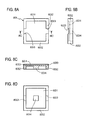
- a silicon substrate having a predetermined shape and size (in this example, a generally square silicon substrate having a predetermined thickness and surface area) is prepared, and as shown in Fig. 9A, silicon dioxide (SiO 2 ) layers 835A and 835B are formed on both the top and bottom surfaces of the silicon substrate 830, respectively, by thermal oxidation.
- silicon dioxide (SiO 2 ) layers 835A and 835B are formed on both the top and bottom surfaces of the silicon substrate 830, respectively, by thermal oxidation.
- a photoresist for example, is applied all over the surface of the silicon dioxide layer 835A over the top surface of the silicon substrate 830, and thereafter, portions of the photoresist corresponding to the shape of the diaphragm 831 and the shapes of the two cutouts 833 are removed respectively by a photoetching process.
- Fig. 9B is a plan view illustrating the state that portions of the silicon dioxide layer 835A corresponding to the shape of the diaphragm 831 and the shapes of the two cutouts 833 have been removed by etching
- Fig. 9C is a sectional view taken along the line 9C-9C in Fig. 9B and looking in the direction indicated by the arrows. This process exposes the top surface of the silicon substrate 830 in the shape of the diaphragm 831 and the shapes of the two cutouts 833.
- Figs. 9D and 9E are plan views thereof and Fig. 9E is a sectional view taken along the line 9E-9E in Fig. 9D and looking in the direction indicated by the arrows.
- the top surface of the silicon substrate is exposed in a generally square portion which will become the top surface of the diaphragm 831 and small rectangular portions corresponding to the two cutouts 833, the generally square frame-like peripheral wall 832 having its height of 5 ⁇ m is formed at the periphery of the top surface of the diaphragm 831, and the two cutouts 833 are formed at substantially symmetrical positions about the center of the diaphragm 831 (at the positions of bilateral symmetry in the drawing).
- a photoresist for example, is applied all over the surface of the silicon dioxide layer 835B over the bottom surface of the silicon substrate 830, and thereafter, a generally square portion of the photoresist corresponding to the shape of the diaphragm 831 except a generally square portion of the photoresist located at the central portion thereof corresponding to the shape of the pedestal mount portion 834 is removed by a photoetching process.
- Fig. 9F is a plan view illustrating the state that a portion of the silicon dioxide layer 835B corresponding to the shape of the diaphragm 831 except a portion thereof corresponding to the shape of the pedestal mount portion 834 has been removed by etching
- Fig. 9G is a sectional view taken along the line 9G-9G in Fig. 9F and looking in the direction indicated by the arrows.
- This process leaves a generally square frame-like silicon dioxide layer 835B and a generally square silicon dioxide layer 835B at the periphery and central portion of the bottom surface of the silicon substrate 830, respectively, and therefore, the bottom surface of the silicon substrate 830 is exposed in the shape of the diaphragm 831 except the central portion of the bottom surface.
- Fig. 9H is a plan view thereof and Fig. 9I is a sectional view taken along the line 9I-9I in Fig. 9H and looking in the direction indicated by the arrows.
- the bottom surface of the silicon substrate is exposed in a generally square portion which will become the bottom surface of the diaphragm 831 except a generally square island-like portion located at the central portion of the silicon substrate, the generally square frame-like peripheral wall 832 having its height of 300 ⁇ m is formed at the periphery of the bottom surface of the diaphragm 831, and the generally square pedestal mount portion 834 having its height of 300 ⁇ m is formed at the central portion of the bottom surface of the diaphragm 831.
- the thickness of the original silicon substrate 830 not etched is selected such that the thickness of the diaphragm 831 falls within the range from several ⁇ m to several tens ⁇ m after it has been etched. Since the thickness of the diaphragm 831 may be changed within a range in which a diaphragm can give a large damping effect to a vibration or oscillation, it is not always limited to the values of the embodiment.
- the optical switch SWB of this embodiment having the above-constructed shock absorbing member 83 attached thereto is used by housing it in a package 9 as shown in Fig. 10.
- the package 9 may be one that has the same construction as that of the prior art package 9 shown in Fig. 4, and is provided with a pedestal 91 on which the optical switch SWB is put and fixed thereto.
- the optical switch SWB is fixed within the package 9 by joining the bottom surface of the pedestal mount portion 834 formed integrally with the bottom surface of the diaphragm 831 of the optical switch SW with the top surface of the pedestal 91 by use of an appropriate adhesive agent, for example.
- a space area S that is an air layer communicating with the outer atmosphere through only the pair of the cutouts 833. Since the space area S acts like an air cushion, its damping effect to a vibration or oscillation is remarkable as well as the diaphragm 831. As a result, if a mechanical vibration or oscillation should be generated in the outside of the optical switch SWB and transmitted to the package 9, the vibration is completely or greatly decreased by the damping effects of the diaphragm 831 and the space area S existing in the way of the vibration transmission path, and hence is substantially not transmitted to the movable electrode plate 2.
- the vibration transmission path in a serial manner constituted by the pedestal 91 of the package 9, the pedestal mount portion 834 of the buffer member 83, the diaphragm 831, the space area S, the stationary electrode substrate 8, the movable electrode supporting frame 10, the connecting portions 211, and the beams 21.
- this vibration transmission path are interposed the diaphragm 831 and the space area S each of which has a large damping effect, and so any external vibration or oscillation applied to the package 9 is completely or almost decreased by the multiplied damping effects of the diaphragm 831 and the space area S.
- the vibration or oscillation is not transmitted to the movable electrode plate 2, or even if it should be transmitted to the movable electrode plate 2, it is decreased to such an extremely weak one that the mirror 3 substantially does not vibrate. Accordingly, there is obtained a remarkable advantage that an optical switch can be provided the operating characteristic of which is not deteriorated even an external vibration or oscillation is transmitted to the package 9.
- the buffer member 83 is a thin and planar-shaped member having the diaphragm 831, it is best suited for a member to be joined with the thin and planar-shaped optical switch part 70.
- the buffer member 83 is attached to the optical switch part 70 having the same construction as that of the prior art optical switch shown in Figs. 1 and 2.
- the buffer member 83 of the above embodiment can be also attached to other known prior art optical switch or switches, and that the same function and effect can be obtained therefrom.
- the buffer member 83 of the above embodiment can be also attached to an optical switch that comprises: a stationary electrode substrate made of an n-type or p-type silicon; two connecting portions; two elastic and flexible beams; and a movable electrode plate supported by the two beams, wherein the two connecting portions, the two elastic and flexible beams, and the movable electrode plate all are made of a p-type or n-type poly-silicon and are formed integrally with one another on the stationary electrode substrate without using a movable electrode supporting frame, and the same function and effect can be obtained therefrom.
- an optical switch that comprises: a stationary electrode substrate made of an n-type or p-type silicon; two connecting portions; two elastic and flexible beams; and a movable electrode plate supported by the two beams, wherein the two connecting portions, the two elastic and flexible beams, and the movable electrode plate all are made of a p-type or n-type poly-silicon and are formed integrally with one another on the stationary electrode substrate without using a
- the number, shape and size of the connecting portions, the number, shape and size of the beams, shapes and sizes of the movable electrode plate, stationary electrode substrate, and the like, or shapes, sizes or the like of the diaphragm, peripheral wall, and cutout of the buffer member are not limited to the illustrated example, and can be modified, altered or changed variously if the need arises.
Landscapes
- Physics & Mathematics (AREA)
- General Physics & Mathematics (AREA)
- Optics & Photonics (AREA)
- Mechanical Light Control Or Optical Switches (AREA)
- Micromachines (AREA)
Applications Claiming Priority (2)
| Application Number | Priority Date | Filing Date | Title |
|---|---|---|---|
| JP2000348378 | 2000-11-15 | ||
| JP2000348378A JP3646250B2 (ja) | 2000-11-15 | 2000-11-15 | 光スイッチ |
Publications (3)
| Publication Number | Publication Date |
|---|---|
| EP1209507A2 true EP1209507A2 (de) | 2002-05-29 |
| EP1209507A3 EP1209507A3 (de) | 2003-05-14 |
| EP1209507B1 EP1209507B1 (de) | 2004-07-28 |
Family
ID=18821976
Family Applications (1)
| Application Number | Title | Priority Date | Filing Date |
|---|---|---|---|
| EP01126549A Expired - Lifetime EP1209507B1 (de) | 2000-11-15 | 2001-11-15 | Optischer Schalter |
Country Status (3)
| Country | Link |
|---|---|
| US (1) | US6560002B2 (de) |
| EP (1) | EP1209507B1 (de) |
| JP (1) | JP3646250B2 (de) |
Cited By (1)
| Publication number | Priority date | Publication date | Assignee | Title |
|---|---|---|---|---|
| CN101880022A (zh) * | 2010-06-08 | 2010-11-10 | 北京大学 | 抗震装置及其制备方法 |
Families Citing this family (10)
| Publication number | Priority date | Publication date | Assignee | Title |
|---|---|---|---|---|
| GB2386030B (en) * | 2000-12-22 | 2004-08-18 | Bruel & Kjaer Sound & Vibratio | A micromachined capacitive transducer |
| US6906846B2 (en) * | 2002-08-14 | 2005-06-14 | Triquint Technology Holding Co. | Micro-electro-mechanical system device and method of making same |
| US7134343B2 (en) * | 2003-07-25 | 2006-11-14 | Kabushiki Kaisha Toshiba | Opto-acoustoelectric device and methods for analyzing mechanical vibration and sound |
| DE102005049731A1 (de) * | 2005-10-14 | 2007-04-19 | Cube Optics Ag | Optischer Aufbau mit elastischer Aufhängung und Verfahren zur Herstellung eines solchen |
| JP4994098B2 (ja) * | 2007-04-25 | 2012-08-08 | 株式会社リコー | 半導体センサ及びその製造方法 |
| JP5377066B2 (ja) * | 2009-05-08 | 2013-12-25 | キヤノン株式会社 | 静電容量型機械電気変換素子及びその製法 |
| JP5349623B2 (ja) * | 2012-01-06 | 2013-11-20 | 株式会社東芝 | 電子機器 |
| US11256083B2 (en) * | 2018-12-27 | 2022-02-22 | Texas Instruments Incorporated | MEMS electrostatic actuator with linearized displacements |
| US12160084B2 (en) | 2019-10-15 | 2024-12-03 | Texas Instruments Incorporated | MEMS-based phase spatial light modulating architecture |
| US12339437B2 (en) | 2019-12-12 | 2025-06-24 | Texas Instruments Incorporated | Bias voltage adjustment for a phase light modulator |
Family Cites Families (14)
| Publication number | Priority date | Publication date | Assignee | Title |
|---|---|---|---|---|
| US5016072A (en) * | 1988-01-13 | 1991-05-14 | The Charles Stark Draper Laboratory, Inc. | Semiconductor chip gyroscopic transducer |
| US5074630A (en) * | 1990-10-09 | 1991-12-24 | Rodino Vincent D | Integrated optics device mounting for thermal and high g-shock isolation |
| US5335304A (en) * | 1993-04-30 | 1994-08-02 | The United States Of America As Represented By The Secretary Of The Army | Connector distribution assembly for a fiber optic detector system |
| JP3799092B2 (ja) * | 1995-12-29 | 2006-07-19 | アジレント・テクノロジーズ・インク | 光変調装置及びディスプレイ装置 |
| GB2321114B (en) * | 1997-01-10 | 2001-02-21 | Lasor Ltd | An optical modulator |
| US6108121A (en) * | 1998-03-24 | 2000-08-22 | The Board Of Trustees Of The Leland Stanford Junior University | Micromachined high reflectance deformable mirror |
| US6147789A (en) * | 1998-05-04 | 2000-11-14 | Gelbart; Daniel | High speed deformable mirror light valve |
| TW457828B (en) * | 1999-03-03 | 2001-10-01 | Tokin Corp | Vibration actuator having magnetic circuit elastically supported by a spiral damper with increased compliance |
| CA2299832C (en) * | 1999-03-04 | 2002-11-12 | Japan Aviation Electronics Industry Limited | Optical switch and method of making the same |
| US6178033B1 (en) * | 1999-03-28 | 2001-01-23 | Lucent Technologies | Micromechanical membrane tilt-mirror switch |
| US6175443B1 (en) * | 1999-05-01 | 2001-01-16 | Lucent Technologies, Inc. | Article comprising a deformable segmented mirror |
| US6275326B1 (en) * | 1999-09-21 | 2001-08-14 | Lucent Technologies Inc. | Control arrangement for microelectromechanical devices and systems |
| JP3910333B2 (ja) * | 2000-03-03 | 2007-04-25 | 富士通株式会社 | ガルバノマイクロミラーとその製造方法 |
| US6480320B2 (en) * | 2001-02-07 | 2002-11-12 | Transparent Optical, Inc. | Microelectromechanical mirror and mirror array |
-
2000
- 2000-11-15 JP JP2000348378A patent/JP3646250B2/ja not_active Expired - Fee Related
-
2001
- 2001-11-14 US US09/992,214 patent/US6560002B2/en not_active Expired - Fee Related
- 2001-11-15 EP EP01126549A patent/EP1209507B1/de not_active Expired - Lifetime
Cited By (2)
| Publication number | Priority date | Publication date | Assignee | Title |
|---|---|---|---|---|
| CN101880022A (zh) * | 2010-06-08 | 2010-11-10 | 北京大学 | 抗震装置及其制备方法 |
| CN101880022B (zh) * | 2010-06-08 | 2012-12-05 | 北京大学 | 抗震装置及其制备方法 |
Also Published As
| Publication number | Publication date |
|---|---|
| EP1209507B1 (de) | 2004-07-28 |
| JP2002148531A (ja) | 2002-05-22 |
| US6560002B2 (en) | 2003-05-06 |
| JP3646250B2 (ja) | 2005-05-11 |
| US20020057484A1 (en) | 2002-05-16 |
| EP1209507A3 (de) | 2003-05-14 |
Similar Documents
| Publication | Publication Date | Title |
|---|---|---|
| US6744550B2 (en) | Two-dimensional micro-mirror array enhancements | |
| EP1209507B1 (de) | Optischer Schalter | |
| US6919980B2 (en) | Mirror rocking member for optical deflector | |
| US8634121B2 (en) | Mirror device, mirror array, optical switch, mirror device manufacturing method, and mirror substrate manufacturing method | |
| US5721377A (en) | Angular velocity sensor with built-in limit stops | |
| US6894787B2 (en) | Optical pressure sensor | |
| US11902740B2 (en) | High-sensitivity piezoelectric microphone | |
| US6888656B2 (en) | Optical deflector | |
| US20030090172A1 (en) | Micro-electro-mechanical-system (mems) mirror device having large angle out of plane motion using shaped combed finger actuators and method for fabricating the same | |
| US5668822A (en) | Integrated semiconductor laser device | |
| US5995525A (en) | Semiconductor laser module | |
| KR19980025006A (ko) | 회전 플레이트를 포함하는 마이크로일렉트로메카닉 장치 및 그 관련 방법 | |
| JP2005011795A (ja) | 非固定の静電的活性型マイクロ電気機械システム・スイッチ | |
| US7164334B2 (en) | Electrostatic actuator, microswitch, micro optical switch, electronic device, and method of manufacturing electrostatic actuator | |
| US20020154374A1 (en) | Vibrator and manufacturing method thereof | |
| EP1346947A2 (de) | Elektrostatisch betriebene optische Schalter- oder Dämpfungsbauelemente | |
| US20030117687A1 (en) | Optical deflector and optical deflector array | |
| WO2001061400A9 (en) | Two-dimensional micro-mirror array enhancements | |
| JP2008026649A (ja) | プレーナー型アクチュエータ、及びそれを用いた光減衰器 | |
| JP4772318B2 (ja) | 光デバイス及びその製造方法 | |
| JP2004319215A (ja) | 静電駆動素子 | |
| JP2981590B2 (ja) | 光スキャナ及びその製造方法 | |
| KR20100110351A (ko) | 미세기계 부품 및 그의 제조 방법 | |
| KR100670945B1 (ko) | Ltcc 기판을 이용한 웨이퍼 규모의 마이크로칼럼어레이 | |
| JPH06103597A (ja) | 集積化光ピックアップ |
Legal Events
| Date | Code | Title | Description |
|---|---|---|---|
| PUAI | Public reference made under article 153(3) epc to a published international application that has entered the european phase |
Free format text: ORIGINAL CODE: 0009012 |
|
| 17P | Request for examination filed |
Effective date: 20011115 |
|
| AK | Designated contracting states |
Kind code of ref document: A2 Designated state(s): AT BE CH CY DE DK ES FI FR GB GR IE IT LI LU MC NL PT SE TR |
|
| AX | Request for extension of the european patent |
Free format text: AL;LT;LV;MK;RO;SI |
|
| PUAL | Search report despatched |
Free format text: ORIGINAL CODE: 0009013 |
|
| AK | Designated contracting states |
Designated state(s): AT BE CH CY DE DK ES FI FR GB GR IE IT LI LU MC NL PT SE TR |
|
| AX | Request for extension of the european patent |
Extension state: AL LT LV MK RO SI |
|
| RIC1 | Information provided on ipc code assigned before grant |
Ipc: 7G 02B 6/35 B Ipc: 7B 81B 3/00 B Ipc: 7G 02B 26/02 A |
|
| 17Q | First examination report despatched |
Effective date: 20030731 |
|
| AKX | Designation fees paid |
Designated state(s): CH FR GB LI |
|
| GRAP | Despatch of communication of intention to grant a patent |
Free format text: ORIGINAL CODE: EPIDOSNIGR1 |
|
| REG | Reference to a national code |
Ref country code: DE Ref legal event code: 8566 |
|
| GRAS | Grant fee paid |
Free format text: ORIGINAL CODE: EPIDOSNIGR3 |
|
| GRAA | (expected) grant |
Free format text: ORIGINAL CODE: 0009210 |
|
| AK | Designated contracting states |
Kind code of ref document: B1 Designated state(s): CH FR GB LI |
|
| REG | Reference to a national code |
Ref country code: GB Ref legal event code: FG4D |
|
| REG | Reference to a national code |
Ref country code: CH Ref legal event code: EP |
|
| REG | Reference to a national code |
Ref country code: IE Ref legal event code: FG4D |
|
| REG | Reference to a national code |
Ref country code: CH Ref legal event code: NV Representative=s name: E. BLUM & CO. PATENTANWAELTE |
|
| ET | Fr: translation filed | ||
| PLBE | No opposition filed within time limit |
Free format text: ORIGINAL CODE: 0009261 |
|
| STAA | Information on the status of an ep patent application or granted ep patent |
Free format text: STATUS: NO OPPOSITION FILED WITHIN TIME LIMIT |
|
| 26N | No opposition filed |
Effective date: 20050429 |
|
| PGFP | Annual fee paid to national office [announced via postgrant information from national office to epo] |
Ref country code: FR Payment date: 20051017 Year of fee payment: 5 |
|
| PGFP | Annual fee paid to national office [announced via postgrant information from national office to epo] |
Ref country code: CH Payment date: 20051111 Year of fee payment: 5 |
|
| PG25 | Lapsed in a contracting state [announced via postgrant information from national office to epo] |
Ref country code: LI Free format text: LAPSE BECAUSE OF NON-PAYMENT OF DUE FEES Effective date: 20061130 Ref country code: CH Free format text: LAPSE BECAUSE OF NON-PAYMENT OF DUE FEES Effective date: 20061130 |
|
| REG | Reference to a national code |
Ref country code: CH Ref legal event code: PL |
|
| GBPC | Gb: european patent ceased through non-payment of renewal fee |
Effective date: 20061115 |
|
| REG | Reference to a national code |
Ref country code: FR Ref legal event code: ST Effective date: 20070731 |
|
| PG25 | Lapsed in a contracting state [announced via postgrant information from national office to epo] |
Ref country code: GB Free format text: LAPSE BECAUSE OF NON-PAYMENT OF DUE FEES Effective date: 20061115 |
|
| PG25 | Lapsed in a contracting state [announced via postgrant information from national office to epo] |
Ref country code: FR Free format text: LAPSE BECAUSE OF NON-PAYMENT OF DUE FEES Effective date: 20061130 |
|
| PGFP | Annual fee paid to national office [announced via postgrant information from national office to epo] |
Ref country code: GB Payment date: 20051109 Year of fee payment: 5 |