EP1207447A2 - Datenverarbeitungsvorrichtung mit der Fähigkeit falsche Daten im Betriebzustand zu verarbeiten und zwecklosen Energieverbrauch im angehaltenen Zustand zu vermeiden - Google Patents
Datenverarbeitungsvorrichtung mit der Fähigkeit falsche Daten im Betriebzustand zu verarbeiten und zwecklosen Energieverbrauch im angehaltenen Zustand zu vermeiden Download PDFInfo
- Publication number
- EP1207447A2 EP1207447A2 EP01250344A EP01250344A EP1207447A2 EP 1207447 A2 EP1207447 A2 EP 1207447A2 EP 01250344 A EP01250344 A EP 01250344A EP 01250344 A EP01250344 A EP 01250344A EP 1207447 A2 EP1207447 A2 EP 1207447A2
- Authority
- EP
- European Patent Office
- Prior art keywords
- data processing
- circuit
- variety
- processing apparatus
- clock
- Prior art date
- Legal status (The legal status is an assumption and is not a legal conclusion. Google has not performed a legal analysis and makes no representation as to the accuracy of the status listed.)
- Withdrawn
Links
Images


Classifications
-
- G—PHYSICS
- G06—COMPUTING OR CALCULATING; COUNTING
- G06F—ELECTRIC DIGITAL DATA PROCESSING
- G06F1/00—Details not covered by groups G06F3/00 - G06F13/00 and G06F21/00
- G06F1/26—Power supply means, e.g. regulation thereof
- G06F1/32—Means for saving power
- G06F1/3203—Power management, i.e. event-based initiation of a power-saving mode
- G06F1/3206—Monitoring of events, devices or parameters that trigger a change in power modality
- G06F1/3228—Monitoring task completion, e.g. by use of idle timers, stop commands or wait commands
-
- G—PHYSICS
- G06—COMPUTING OR CALCULATING; COUNTING
- G06F—ELECTRIC DIGITAL DATA PROCESSING
- G06F1/00—Details not covered by groups G06F3/00 - G06F13/00 and G06F21/00
- G06F1/26—Power supply means, e.g. regulation thereof
- G06F1/32—Means for saving power
- G06F1/3203—Power management, i.e. event-based initiation of a power-saving mode
- G06F1/3234—Power saving characterised by the action undertaken
- G06F1/3243—Power saving in microcontroller unit
-
- Y—GENERAL TAGGING OF NEW TECHNOLOGICAL DEVELOPMENTS; GENERAL TAGGING OF CROSS-SECTIONAL TECHNOLOGIES SPANNING OVER SEVERAL SECTIONS OF THE IPC; TECHNICAL SUBJECTS COVERED BY FORMER USPC CROSS-REFERENCE ART COLLECTIONS [XRACs] AND DIGESTS
- Y02—TECHNOLOGIES OR APPLICATIONS FOR MITIGATION OR ADAPTATION AGAINST CLIMATE CHANGE
- Y02D—CLIMATE CHANGE MITIGATION TECHNOLOGIES IN INFORMATION AND COMMUNICATION TECHNOLOGIES [ICT], I.E. INFORMATION AND COMMUNICATION TECHNOLOGIES AIMING AT THE REDUCTION OF THEIR OWN ENERGY USE
- Y02D10/00—Energy efficient computing, e.g. low power processors, power management or thermal management
Definitions
- the present invention relates to a data processing apparatus which is capable of executing a variety of operations as well as dealing with illegal external inputs in an operative state, and temporarily stopping components associated with the operations to prevent useless power consumption in a stopped state.
- ALU Arimetic and Logical Unit
- portable data processing apparatuses which are mounted on a data processing terminal station and operated integrally therewith. In some cases, such portable data processing apparatuses do not internally generate a clock signal but are supplied with a clock signal from associated data processing terminal stations. Also, since portable data processing apparatuses generally use a battery as a power source, some of them stop useless data processing to save power consumption.
- a data processing apparatus 100 illustrated herein comprises ALU 101 as a data processing circuit which is connected to bus line 102.
- program memory 103 Connected to bus line 102 are program memory 103, data memory 104, general register 105, a plurality of I/Os (Input/Output) 1.06, and so on.
- Program memory 103 is connected to program counter 107 and decoder 108.
- Decoder 108 is connected to standby controller 109 which functions as an operation control circuit.
- Standby controller 109 in turn is connected to INT (Interrupt) 110 and IAD (Illegal Access Detector) 111 which functions as an input monitor circuit.
- INT Interrupt
- IAD Illegal Access Detector
- Data processing apparatus 100 is formed as a portable type one which is mounted to a separate data processing terminal station (not shown), and also has an external input terminal and a clock input terminal (not shown).
- the external input terminal is connected to an external output terminal of the data processing terminal station to receive a variety of data and a variety of signals from the data processing terminal station, while the clock input terminal is connected to a clock output terminal of the data processing terminal station to receive a clock signal from the data processing terminal station.
- Program memory 103 comprises, for example, an EEPROM (Electrically Erasable Programmable Read Only Memory) or a flash memory, and stores an operation program comprising a variety of instructions.
- EEPROM Electrically Erasable Programmable Read Only Memory
- flash memory stores an operation program comprising a variety of instructions.
- Program counter 107 is responsive to a variety of signals fed through the external input terminal from the outside, for example, to specify an address in program memory 103 at which an instruction to be executed is stored.
- Decoder 108 reads an instruction from program memory 103 at an address specified by program counter 107, and decodes this instruction to generate a variety of control signals which are then supplied to associated components such as ALU 101.
- ALU 101 executes a variety of data processing in synchronization with the clock signal fed through the clock input terminal from the outside corresponding to a variety of data fed through the external input terminal from the outside; a variety of data temporarily stored in data memory 104; an operation program supplied thereto from program memory 103 through decoder 108; and so on.
- Data memory 104 comprising, e.g. a RAM (Random Access Memory), temporarily stores data which is to be processed by ALU 101.
- General register 105 comprising a general-purpose register, temporarily holds a variety of data before processing, in the middle of processing, and after the processing.
- I/Os 106 which are peripheral circuits each having a variety of functions are integrally controlled by ALU 101.
- IAD 111 monitors a variety of data and a variety of signals fed from the outside, and executes predetermined counter-operations such as resetting of the entire apparatus, when it determines an external input as improper.
- INT 110 receives an interrupt signal fed from the outside, an interrupt signal internally generated by any I/O 106, and so on, and instructs ALU 101 or standby controller 109 to execute interrupt processing corresponding to a received interrupt signal.
- Standby controller 109 temporarily stops the components such as IAD 111, ALU 101 and I/Os 106 in response to a predetermined condition, for example, execution of a stop instruction, and so on, and restarts such temporarily stopped components in response to a predetermined condition such as an interrupt fed to INT 110.
- Data processing apparatus 100 configured as described above can be mounted to a separate data processing terminal station, and execute a variety of data processing in accordance with a variety of data and a clock signal supplied thereto from the data processing terminal station.
- program counter 107 specifies an address in program memory 103 in response to a variety of externally fed signals, an instruction at this specified address is read from program memory 103 and decoded to a control signal by decoder 108.
- control signal is supplied to associated components such as ALU 101, which, for example, executes a variety of data processing in synchronization with the clock signal fed through the clock input terminal from the external data processing terminal station in accordance with a variety of data fed through the external input terminal from the external data processing terminal station and an operation program supplied from program memory 103 through decoder 108.
- ALU 101 executes a variety of data processing in synchronization with the clock signal fed through the clock input terminal from the external data processing terminal station in accordance with a variety of data fed through the external input terminal from the external data processing terminal station and an operation program supplied from program memory 103 through decoder 108.
- IAD 111 a variety of data and a variety of signals fed to dataprocessing apparatus 100 from the outside as described above are monitored at all times by IAD 111, so that if an illegal input, such as an input which does not comply with a standard, is detected by IAD 111, IAD 111 resets the entire apparatus.
- a stop instruction in program memory 103 is decoded to a stop signal by decoder 108 in response to a predetermined condition.
- This stop signal is supplied to standby controller 109.
- standby controller 109 Upon receipt of the stop signal, standby controller 109 temporarily stops the components such as IAD 111, ALU 101 and I/Os 106, thereby making it possible to prevent use less power consumption in this stopped state.
- INT 110 restarts temporarily stopped components in response to a predetermined condition such as an interrupt fed thereto even in a stopped state, this permits data processing apparatus 100 to restore a normal operative state.
- Data processing apparatus 100 as described above can temporarily stop its components such as ALU 101 and IAD 111 to prevent useless power consumption, restore a normal operative state even from the stopped state, and deal with illegal external inputs by means of IAD 111 in the normal operative state.
- IAD 111 since IAD 111 is also inoperative when stopped, data processing apparatus 100 cannot deal with illegal external inputs. To solve this problem, it is contemplated that IAD 111 is left operative at all times, in which case, however, IAD 111 consumes power even in a stopped state.
- the present invention has been made in view of the problem as mentioned above, and its object is to provide at least one of a data processing apparatus and system which are capable of dealing with illegal external inputs without consuming power uselessly when in a stopped state.
- an operation program comprising a variety of instructions is stored in a program memory, so that when a variety of data and a variety of signals are fed to an external input terminal from the outside and a clock signal is fed to a clock input terminal from the outside, a data processing circuit executes a variety of data processing in synchronization with the externally fed clock signal in accordance with the variety of externally fed data and the operation program stored in the program memory.
- an input monitor circuit is monitoring the variety of data and the variety of signals fed from the outside, and executes a predetermined counter-operation when it determines any of them are improper, so that the data processing apparatus can deal with an illegal external input in an operative state. Also, since an operation control circuit controls operations involved in temporarily stopping and restarting the input monitor circuit and data processing circuit, it is possible to prevent useless power consumption in a stopped state, and also restore an operative state from the stopped state.
- a clock counter circuit counts a clock signal fed through the clock input terminal from the outside while the operation control circuit temporarily stops the input monitoring circuit and data processing circuit, and as the count number of the clock counter circuit reaches a predetermined number, a monitor start circuit restarts the input monitor circuit temporarily stopped by the operation control circuit.
- the data processing apparatus can deal with an illegal external input even in a stopped state when the externally fed clock signal reaches the predetermined count, and can even prevent a useless increase in power consumption in a stopped state since the clock counter circuit consumes an extremely small amount of power.
- a predetermined count number has been set in a register circuit, and a comparator compares the set count number with the count number of the clock counter circuit.
- the monitor start circuit can be implemented in a simple configuration which restarts the temporarily stopped input monitoring circuit when the count number of the clock counter circuit reaches the predetermined number.
- the register circuit updatably stores the count number of the externally fed clock, a desired count number can be set in the register circuit, so that the security level can be freely adjusted, thereby making it possible to satisfy both a user who prefers power saving to security and a user who prefers security to power saving.
- a data processing terminal station externally feeds the data processing apparatus of the present invention with a variety of data, a variety of signals, and a clock signal
- the data processing apparatus of the present invention can communicate data with the data processing terminal station to execute a variety of data processing.
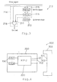
- data processing apparatus 200 is formed as a component of data processing system 400, together with separate data processing terminal station 300, and is implemented as a portable apparatus which is mounted to data processing terminal station 300 and operated integrally therewith, similarly to data processing apparatus 100 described above as a prior art example.
- Data processing terminal station 300 has external output terminal 301 for feeding a variety of data and a variety of signals to the outside; and clock output terminal 302 for feeding a clock signal to the outside.
- Data processing apparatus 200 in turn has external input terminal 201 for receiving a variety of data and a variety of signals from the outside; and clock input terminal 202 for receiving a clock signal from the outside.
- data processing apparatus 200 also has an ALU 101 as a data processing circuit, program memory 103, data memory 104, general register 105, a plurality of I/Os 106, and so on connected to bus line 102, and program memory 103 is connected to program counter 107 and decoder 108, similarly to the prior art example.
- Decoder 108 is connected to standby controller 211, which functions as an operation control circuit, and standby controller 211 is connected to INT 110 and IAD 111 which functions as an input monitor circuit.
- stop control circuit 212 is inserted in a communication path through which a stop signal is sent from decoder 108 to standby controller 211.
- stop control circuit 212 comprises clock counter circuit 213 and monitor start circuit 214.
- Monitor start circuit 214 comprises register circuit 215, comparator circuit 216, invertor device 217, and AND gate 218.
- Clock counter circuit 213 counts a clock signal fed through clock input terminal 202 from the outside while standby controller 211 temporarily stops IAD 111 and ALU 101.
- Register circuit 215 updatably stores the count number of the externally fed clock signal, and comparator circuit 216 compares a count number set in register circuit 215 with the count number of clock counter circuit 213.
- Invertor device 217 inverts the result of comparison from comparator circuit 216, and supplies the inverted result to one of a pair of input terminals of AND gate 218.
- AND gate 218 inverts a stop signal supplied to standby controller 211 in response to the data supplied thereto.
- standby controller 211 temporarily stops the components such as IAD 111, ALU 101, I/Os 106, and otherwise in response to a predetermined condition, and restarts the temporarily stopped component in response to a predetermined condition.
- standby controller 211 is responsive to inversion of the stop signal, when components such as IAD 111, ALU 101 I/Os 106, and otherwise are temporarily stopped, to restart IAD 111 alone while maintaining ALU 101, I/Os 106 and so on in a stopped state.
- data processing apparatus 200 of this embodiment actually has the foregoing main circuits integrated as single MPU (Microprocessor Unit) 220 to which are connected a plurality of I/Os 106, a variety of input terminals 201, 202, and so on.
- MPU Microprocessor Unit
- data processing apparatus 200 of this embodiment can execute a variety of data processing in accordance with a variety of data and clock signals externally fed thereto from separate data processing terminal station 300, similarly to data processing apparatus 100.
- data processing apparatus 200 can temporarily stop the components such as ALU 101, IAD 111, and otherwise to prevent useless power consumption, restore a normal operative state from the stopped state through restarting, and deal with illegal external inputs by the action of IAD 111 in a normal operative state.
- data processing apparatus 200 of this embodiment differs from data processing apparatus 100 in that as a clock signal is fed from the outside in a stopped state, the clock signal is counted by clock counter circuit 213, and the count number is compared with the count number set in register circuit 215 by comparator circuit 216.
- the stop signal is inverted by AND gate 218, so that standby controller 211 restarts IAD 111 alone in response to the inversion while maintaining ALU 101 and otherwise in a stopped state.
- data processing apparatus 200 of this embodiment can deal with illegal external inputs because IAD 111 is restarted when the externally fed clock signal reaches a predetermined number even in a stopped state, thereby providing high security even in a stopped state.
- IAD 111 is not left operated continuously in a stopped state, so that the power will not be uselessly consumed in a stopped state.
- the security level can be freely adjusted, thereby making it possible to satisfy both of a user who prefers power saving to security and a user who prefers security to power saving.
- standby controller 211 restarts only IAD 111 in a stopped state as stop control circuit 212 inverts the stop signal in a stopped state.
- stop control circuit 212 may directly restart IAD 111 in a stopped state without intervention of standby controller 211.
Landscapes
- Engineering & Computer Science (AREA)
- Theoretical Computer Science (AREA)
- Physics & Mathematics (AREA)
- General Engineering & Computer Science (AREA)
- General Physics & Mathematics (AREA)
- Power Sources (AREA)
- Calculators And Similar Devices (AREA)
Applications Claiming Priority (2)
| Application Number | Priority Date | Filing Date | Title |
|---|---|---|---|
| JP2000319287A JP4439711B2 (ja) | 2000-10-19 | 2000-10-19 | データ処理装置およびシステム |
| JP2000319287 | 2000-10-19 |
Publications (2)
| Publication Number | Publication Date |
|---|---|
| EP1207447A2 true EP1207447A2 (de) | 2002-05-22 |
| EP1207447A3 EP1207447A3 (de) | 2004-10-13 |
Family
ID=18797774
Family Applications (1)
| Application Number | Title | Priority Date | Filing Date |
|---|---|---|---|
| EP01250344A Withdrawn EP1207447A3 (de) | 2000-10-19 | 2001-09-27 | Datenverarbeitungsvorrichtung mit der Fähigkeit falsche Daten im Betriebzustand zu verarbeiten und zwecklosen Energieverbrauch im angehaltenen Zustand zu vermeiden |
Country Status (3)
| Country | Link |
|---|---|
| US (1) | US6813713B2 (de) |
| EP (1) | EP1207447A3 (de) |
| JP (1) | JP4439711B2 (de) |
Families Citing this family (4)
| Publication number | Priority date | Publication date | Assignee | Title |
|---|---|---|---|---|
| KR100976861B1 (ko) | 2008-01-21 | 2010-08-23 | 주식회사 안철수연구소 | 하드웨어를 통해 발생하는 자동 입력 감지 방법 및 그 장치 |
| KR101005593B1 (ko) | 2009-04-17 | 2011-01-05 | 엔에이치엔비즈니스플랫폼 주식회사 | 훅을 이용한 컴퓨터 보안 서비스 제공 방법 및 장치 |
| EP2738559B1 (de) * | 2012-11-28 | 2020-01-08 | Siemens Healthcare Diagnostics Products GmbH | Verfahren zum vorübergehenden Betrieb eines automatischen Analysegeräts in einem Bereitschaftsmodus |
| EP3022653B1 (de) | 2013-07-18 | 2020-12-02 | NXP USA, Inc. | Fehlerdetektionsvorrichtung und -verfahren |
Family Cites Families (7)
| Publication number | Priority date | Publication date | Assignee | Title |
|---|---|---|---|---|
| JPH03218130A (ja) * | 1990-01-24 | 1991-09-25 | Fuji Electric Co Ltd | 光信号入力形の機器 |
| JPH0462614A (ja) * | 1990-06-30 | 1992-02-27 | Nec Home Electron Ltd | 携帯型データ処理装置 |
| JP2842750B2 (ja) * | 1992-04-07 | 1999-01-06 | 三菱電機株式会社 | Icカード |
| US5293424A (en) * | 1992-10-14 | 1994-03-08 | Bull Hn Information Systems Inc. | Secure memory card |
| US5715256A (en) * | 1996-09-27 | 1998-02-03 | Sun Microsystems, Inc. | Method and apparatus for handling multiplexer contention during scan |
| FR2775090B1 (fr) * | 1998-02-13 | 2000-12-29 | Roland Moreno | Objet portatif de type carte a microcircuit comprenant des moyens de supervision des commandes qui lui sont appliquees |
| US6266773B1 (en) * | 1998-12-31 | 2001-07-24 | Intel. Corp. | Computer security system |
-
2000
- 2000-10-19 JP JP2000319287A patent/JP4439711B2/ja not_active Expired - Fee Related
-
2001
- 2001-09-27 EP EP01250344A patent/EP1207447A3/de not_active Withdrawn
- 2001-10-04 US US09/970,528 patent/US6813713B2/en not_active Expired - Lifetime
Also Published As
| Publication number | Publication date |
|---|---|
| US20020049921A1 (en) | 2002-04-25 |
| JP4439711B2 (ja) | 2010-03-24 |
| US6813713B2 (en) | 2004-11-02 |
| EP1207447A3 (de) | 2004-10-13 |
| JP2002132395A (ja) | 2002-05-10 |
Similar Documents
| Publication | Publication Date | Title |
|---|---|---|
| US5189647A (en) | Information processing system having power saving control of the processor clock | |
| US7007180B2 (en) | System and method for switching a computer system to a first or second power saving mode based on whether or not there exists a timer-expiration-waiting event in an event queue | |
| US20090119526A1 (en) | Electronic system and power control method thereof | |
| US6178523B1 (en) | Battery-operated device with power failure recovery | |
| KR20090026895A (ko) | 시스템 온 칩에서 전력 소모를 감소시키기 위한 장치 및방법 | |
| JPH07200092A (ja) | コンピュータシステムおよびその電力管理装置 | |
| JPH10177563A (ja) | フラッシュメモリ内蔵マイクロコンピュータ | |
| CN115756622B (zh) | 芯片控制方法及芯片 | |
| US10719331B2 (en) | Stand-by mode of an electronic circuit | |
| US6813713B2 (en) | Data processing apparatus capable of dealing with illegal external input in an operative state and preventing useless power consumption in a stopped state | |
| US7516347B2 (en) | Electronic device having power-down mode and method of reducing power consumption | |
| US7986168B2 (en) | Semiconductor apparatus and anomaly detection method of the same | |
| CN116700469A (zh) | 一种设备保活方法、装置及相关设备 | |
| JP3214469B2 (ja) | マイクロコンピュータによるフラッシュeepromの書き込み制御方法及び装置 | |
| KR102262438B1 (ko) | 차량용 멀티미디어 서비스 기기의 전원 제어 장치 및 방법 | |
| JP4647276B2 (ja) | 半導体回路装置 | |
| JPH0756774A (ja) | ウォッチドッグタイマ | |
| JPH06202764A (ja) | 電源切断装置 | |
| JPH09190360A (ja) | マイクロコンピュータ及びその暴走監視処理方法 | |
| JPS6389941A (ja) | マイクロプロセツサ応用機器の監視制御装置 | |
| JPH11119872A (ja) | 電源電圧検出回路 | |
| KR100269348B1 (ko) | 자동 리-스타트(re-start)회로를 구비한 무선 랜(lan) 시스템 | |
| JPH10271690A (ja) | 携帯型電子装置及びその電池充電方法 | |
| CN121807389A (zh) | 芯片控制方法、装置、电子设备及车辆 | |
| JPS63271545A (ja) | ウオツチドツグタイマ |
Legal Events
| Date | Code | Title | Description |
|---|---|---|---|
| PUAI | Public reference made under article 153(3) epc to a published international application that has entered the european phase |
Free format text: ORIGINAL CODE: 0009012 |
|
| AX | Request for extension of the european patent |
Free format text: AL;LT;LV;MK;RO;SI |
|
| RAP1 | Party data changed (applicant data changed or rights of an application transferred) |
Owner name: NEC ELECTRONICS CORPORATION |
|
| PUAL | Search report despatched |
Free format text: ORIGINAL CODE: 0009013 |
|
| AK | Designated contracting states |
Kind code of ref document: A3 Designated state(s): AT BE CH CY DE DK ES FI FR GB GR IE IT LI LU MC NL PT SE TR |
|
| AX | Request for extension of the european patent |
Extension state: AL LT LV MK RO SI |
|
| 17P | Request for examination filed |
Effective date: 20041015 |
|
| 17Q | First examination report despatched |
Effective date: 20050506 |
|
| AKX | Designation fees paid |
Designated state(s): DE FR GB |
|
| STAA | Information on the status of an ep patent application or granted ep patent |
Free format text: STATUS: THE APPLICATION IS DEEMED TO BE WITHDRAWN |
|
| 18D | Application deemed to be withdrawn |
Effective date: 20050917 |