EP1205280A1 - Wafer polishing method and wafer polishing device - Google Patents
Wafer polishing method and wafer polishing device Download PDFInfo
- Publication number
- EP1205280A1 EP1205280A1 EP00981769A EP00981769A EP1205280A1 EP 1205280 A1 EP1205280 A1 EP 1205280A1 EP 00981769 A EP00981769 A EP 00981769A EP 00981769 A EP00981769 A EP 00981769A EP 1205280 A1 EP1205280 A1 EP 1205280A1
- Authority
- EP
- European Patent Office
- Prior art keywords
- wafer
- adhered
- adhering
- holding plate
- polished
- Prior art date
- Legal status (The legal status is an assumption and is not a legal conclusion. Google has not performed a legal analysis and makes no representation as to the accuracy of the status listed.)
- Granted
Links
Images



Classifications
-
- H—ELECTRICITY
- H10—SEMICONDUCTOR DEVICES; ELECTRIC SOLID-STATE DEVICES NOT OTHERWISE PROVIDED FOR
- H10P—GENERIC PROCESSES OR APPARATUS FOR THE MANUFACTURE OR TREATMENT OF DEVICES COVERED BY CLASS H10
- H10P50/00—Etching of wafers, substrates or parts of devices
-
- B—PERFORMING OPERATIONS; TRANSPORTING
- B24—GRINDING; POLISHING
- B24B—MACHINES, DEVICES, OR PROCESSES FOR GRINDING OR POLISHING; DRESSING OR CONDITIONING OF ABRADING SURFACES; FEEDING OF GRINDING, POLISHING, OR LAPPING AGENTS
- B24B37/00—Lapping machines or devices; Accessories
- B24B37/27—Work carriers
- B24B37/30—Work carriers for single side lapping of plane surfaces
-
- B—PERFORMING OPERATIONS; TRANSPORTING
- B25—HAND TOOLS; PORTABLE POWER-DRIVEN TOOLS; MANIPULATORS
- B25B—TOOLS OR BENCH DEVICES NOT OTHERWISE PROVIDED FOR, FOR FASTENING, CONNECTING, DISENGAGING, OR HOLDING
- B25B11/00—Work holders not covered by any preceding group in the subclass, e.g. magnetic work holders, vacuum work holders
- B25B11/005—Vacuum work holders
-
- H—ELECTRICITY
- H10—SEMICONDUCTOR DEVICES; ELECTRIC SOLID-STATE DEVICES NOT OTHERWISE PROVIDED FOR
- H10P—GENERIC PROCESSES OR APPARATUS FOR THE MANUFACTURE OR TREATMENT OF DEVICES COVERED BY CLASS H10
- H10P72/00—Handling or holding of wafers, substrates or devices during manufacture or treatment thereof
- H10P72/70—Handling or holding of wafers, substrates or devices during manufacture or treatment thereof for supporting or gripping
- H10P72/78—Handling or holding of wafers, substrates or devices during manufacture or treatment thereof for supporting or gripping using vacuum or suction, e.g. Bernoulli chucks
-
- H—ELECTRICITY
- H10—SEMICONDUCTOR DEVICES; ELECTRIC SOLID-STATE DEVICES NOT OTHERWISE PROVIDED FOR
- H10P—GENERIC PROCESSES OR APPARATUS FOR THE MANUFACTURE OR TREATMENT OF DEVICES COVERED BY CLASS H10
- H10P52/00—Grinding, lapping or polishing of wafers, substrates or parts of devices
- H10P52/40—Chemomechanical polishing [CMP]
- H10P52/402—Chemomechanical polishing [CMP] of semiconductor materials
Definitions
- thickness unevenness of an adhesive layer generates in an adhesion portion. It is considered that the thickness unevenness is caused by surface roughness and fine structure of the wafer holding plate, physical property of an interface between the adhesive and the ceramic, or the like. The thickness unevenness causes unfavorable ununiformity of the thickness in the wafer after polishing.
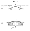
- the surface to be adhered of the wafer W on the wafer adhering apparatus of the earlier developed technique has the concave surface portion as shown in FIG. 3(a).
- the wafer adhering apparatus of the first embodiment as shown FIG. 3(b)
- the surface to be adhered of the wafer W swells so as to form the convex surface as a whole, and the surface to be adhered of the wafer W does not have the concave surface portion. As a result, remaining of the trace amount of air between the surface to be adhered of the wafer W and the wafer holding plate is prevented.
- the surface of the contacting member 32 may be provided with a small hole or grooves for discharging air.
- the wafer may be chucked to be held by vacuum-sucking the wafer W through the small hole or grooves.
- FIG. 7 shows the wafer holding plate according to the fourth embodiment of the present invention.
- the structure of the wafer holding plate 40 according to the fourth embodiment will be explained.
- the wafer holding plate 40 comprises, as shown in the figure, a base member of a ceramic plate 40a having a diameter of 630mm and a thickness of 20mm, which are not particularly limited to, and a glass plate 40b having a diameter of 630mm and a thickness of 1mm to 20mm, which are not particularly limited to.
- the wafer W is adhered to a surface of the latter glass plate 40b, the surface being not bonded with the ceramic plate 40a.
- the ceramic plate 40a of the wafer holding plate 40 constructed as above-described is hard to bend because it has high rigidity compared with the glass plate 40b.
- the wafer holding plate 40 has both advantages of rigidity of ceramic and excellent adhesion property against the wafer W. Thus, the flatness in the polishing can be improved.
- a slurry nozzle 74 is located above the central portion of the polishing turn table 72.
- the slurry nozzle 74 is connected with a slurry supplying device (not shown).
- the abrasive slurry is appropriately supplied to the slurry nozzle 74 from the slurry supplying device.
- alkaline solution including abrasive grains of colloidal silica is supplied, which is not particularly limited to.
- the present invention is not limited to the embodiments and examples, and various modifications may be made within the scope of the invention.
- the present invention can be applied to a polishing of other thin plate products, such as magnetic disc substrates, quartz glass substrates or the like.
Landscapes
- Engineering & Computer Science (AREA)
- Mechanical Engineering (AREA)
- Finish Polishing, Edge Sharpening, And Grinding By Specific Grinding Devices (AREA)
- Mechanical Treatment Of Semiconductor (AREA)
- Constituent Portions Of Griding Lathes, Driving, Sensing And Control (AREA)
- Grinding And Polishing Of Tertiary Curved Surfaces And Surfaces With Complex Shapes (AREA)
- Container, Conveyance, Adherence, Positioning, Of Wafer (AREA)
Abstract
Description
- The present invention relates to a method for polishing a wafer and an apparatus for polishing a wafer, and furthermore to a wafer holding plate, a wafer adhering method and a wafer adhering apparatus that are used for the method and apparatus for polishing a wafer.
- Reflecting increasing a diameter of a silicon wafer and improving of high accuracy of a device fabricated by employing it, the requirements for final accuracy (thickness uniformity, flatness and smoothness) of a silicon wafer (polished wafer) which is polished for finish are becoming higher.
- In order to satisfy such requirements, techniques of polishing process for wafer have been improved, and apparatuses for the polishing process have been developed and improved.
- As one of them, so-called single wafer polishing apparatuses have been freshly developed for the purpose of polishing a wafer having a large diameter of, particularly 300mm or more, and some of them are put to practical use.
- However, with the single wafer polishing method, problems that (1) it is difficult to meet the requirement for a reduction of wafer costs in view of productivity, (2) it is difficult to meet the recent requirement for flatness in the vicinity of peripheral edge of the wafer (within 1mm from peripheral outer edge), or the like have arisen.
- On the other hand, with a polishing method by a batch processing polishing apparatus in which a plurality of wafers are adhered to a wafer holding plate with adhesive, and then polished simultaneously, which is popularized most, the constitution and structures of the apparatus and performance thereof are being improved for achieving the high accurate finish. However, there is the following problem according to the adhesion mounting of the wafer on the wafer holding plate via adhesive.
- That is, although ceramic materials have employed for the wafer holding plate, for example, with a wafer holding plate made of sintered ceramic including alumina as the main component, thickness unevenness of an adhesive layer generates in an adhesion portion. It is considered that the thickness unevenness is caused by surface roughness and fine structure of the wafer holding plate, physical property of an interface between the adhesive and the ceramic, or the like. The thickness unevenness causes unfavorable ununiformity of the thickness in the wafer after polishing.
- On the other hand, with a wafer holding plate made of glass, the above-described problem of the thickness unevenness of the adhesive layer in the adhesion portion is avoided. However, when the wafer is pressed against a polishing pad during polishing, the glass bends, causing excess polishing of the peripheral portion of the wafer compared to other portions. Thus, the flatness of the wafer lowers.
- Further, when the wafer is adhered to the wafer holding plate, very small amount of air remains between the wafer holding plate and the wafer. A portion of a surface to be polished of the wafer, which is corresponding to a portion sandwiching the remained air bubble, protuberates slightly, and is polished extra. As a result, the thickness unevenness of the wafer and the lowering of the flatness of the polished surface are caused.
- In order to solve this problem, a jig that curves the wafer so that the air between the wafer and the wafer holding plate will be let out from the center of the wafer toward the periphery of the wafer, and that is for adhering the wafer to the wafer holding plate from the center of the wafer has been developed. However, with the jig having the previous structure, a surface to be adhered of the wafer does not become a uniform convex surface, but a part of the surface to be adhered forms a concave surface portion. Thereby, the air remains in the concave surface portion, and thus the problem is not solved completely.
- Furthermore, particularly, with the wafer holding plate used for the batch processing polishing apparatus, since the wafer is adhered to the wafer holding plate at an eccentric position, even if the wafer holding plate is rotated inductively, rubbing rates vary in-plane in a single wafer against the polishing pad. Thus, the peripheral portion of the wafer is excessively polished compared to the central portion thereof. This is a factor obstructive to the improvement of the flatness of the wafer.
- For solving the problems caused by the adhesion of the wafer described above, investigations and trial manufactures were repeatedly carried out eagerly. Then, it was achieved developing an adhering method and an adhering apparatus that let out the air between the wafer and the wafer holding plate during the adhesion by forming the surface to be adhered of the wafer into the convex surface as a whole, and then do not make an air bubble remain.
- With the adhering method and the adhering apparatus, the wafer is held by vacuum-chucking the surface to be polished of a wafer such that a convex surface is formed in the vicinity including an arbitrary point within a region surrounding the center of the surface to be adhered of the wafer, and the region being at least not less than 50% of the entire adhesion area, and the wafer is adhered to the wafer holding plate from the central portion of the surface to be adhered of the wafer.
- When the wafer is curved so as to form such convex surface, it is preferable that a wafer contacting region of a wafer holding surface of a contacting member has a value of radius of curvature between 5m and 1000m, the radius of curvature being for a line of intersection between a plane which includes a normal line of an arbitrary point and which passes through a center of the wafer contacting region and the wafer contacting region, within a region surrounding the center of the wafer contacting region and corresponding to at least not less than 50% of the entire adhesion area of the wafer. Furthermore, it is preferable that the surface to be adhered of the wafer is made such that a value of radius of curvature of a line of intersection between a plane including a normal line of an arbitrary point and passing through a center of the surface to be adhered and the surface to be adhered is between 5m and 1000m, within a surface which surrounds the center of the surface to be adhered and which is at least not less than 50%. The reason therefor is that when the value of radius of curvature is less than 5m, problems that 1 ○ when the vacuum-chuck is released, because a restoring force of the wafer is large, the peripheral portion of the wafer is immediately brought into contact with the wafer holding plate, thereby the air between the wafer holding plate and the wafer is not removed sufficiently, 2 ○ excessive stress generates inside of the wafer, 3 ○ it is required to increase the vacuum-sucking force for the wafer, or the like arise. On the other hand, the reason therefor is that when the value of the radius of curvature is more than 1000m, there are problems that the peripheral portion of the wafer is brought into contact with the wafer holding plate before the air in the center lets out, thereby the air between the wafer holding plate and the wafer is not removed sufficiently, or the like.
- As a concrete method for forming the surface to be adhered of the wafer into the above-described convex surface, the wafer holding surface itself of the contacting member chucking the surface to be polished of the wafer may be formed into the convex surface, or the contacting member chucking the surface to be polished of the wafer may be transformed by a pressure applying means such that the surface to be adhered of the wafer forms the convex surface. In the latter case, for example, an air supply and discharge apparatus is used as the pressure applying means.
- On the other hand, at first, the wafer can be held by vacuum-chucking only in the peripheral portion of the surface to be polished of the wafer. In this case, it may be preferable that the wafer may be held by vacuum-chucking with a plurality of holders having sucking disk structure. When the vacuum-chuck holding is carried out with the plurality of holders, each chucked area can be reduced all the better for that. Thus, no concave surface portion generates in the surface to be adhered of the wafer.
- Alternatively, holding of the wafer by vacuum-chucking may be carried out by vacuum-sucking the surface to be adhered of the wafer through a small hole for discharging air, the small hole being provided to the contacting member, or by vacuum-sucking the surface to be adhered of the wafer through a groove formed in the wafer holding surface of the contacting member.
- The contacting member may be made of ceramic, polymeric material or metallic material, for example. When the metallic material is employed, at least a wafer holding surface of the contacting member is coated with nonmetallic material.
- The inventors made various developments and trial manufactures for solving the thickness unevenness of the adhesive layer in the adhesion portion when the wafer is adhered to the wafer holding plate made of ceramic. The inventors developed a wafer holding plate that is capable of combining rigidity of ceramic and an excellent adhesion property of the wafer holding plate made of glass, and then achieved obtaining a high accurate polished wafer by applying a polishing method and a polishing apparatus to which these development results are adapted.
- For example, a base member of the wafer holding plate is made of ceramic and a surface for adhering a wafer comprises a glass layer. Alternatively, the base member is made of ceramic and a side for adhering a wafer is provided with a glass plate. In this case, it is preferable that the glass comprises borosilicate glass. Furthermore, it is preferable that the glass layer has a thickness between 0.05mm and 2mm, and the glass plate has a thickness between 1mm and 20mm.
- Further, adhering the wafer to the wafer holding plate combining the rigidity and the adhesion property by using the improved adhering method and adhering apparatus, and then polishing the wafer has a remarkable effect on improvement of the flatness of the wafer.
- Furthermore, when a wafer holding portion of a wafer holding plate employed for the batch processing polishing apparatus is turnable with respect to a base body, the surface to be polished of the wafer comes more uniformly in contact with the polishing pad. Therefore, it has much effect on improvement of the flatness.
- When the wafer is adhered to the wafer holding plate, it is preferable that a wafer is adhered while holding the wafer such that difference of elevation of the surface to be adhered of the wafer is between 20µm and 1000µm. The reason therefor is that when the difference of elevation is more than 1000µm, problems that 1 ○ when the vacuum-chuck is released, because a restoring force of the wafer is large, the peripheral portion of the wafer is immediately brought into contact with the wafer holding plate, thereby the air between the wafer holding plate and the wafer is not removed sufficiently, 2 ○ excessive stress generates inside of the wafer, 3 ○ it is required to increase the vacuum-sucking force for the wafer, or the like arise. On the other hand, the reason therefor is that when the difference of elevation is less than 20µm, there are problems that the peripheral portion of the wafer is brought into contact with the wafer holding plate before the air in the center lets out, thereby the air between the wafer holding plate and the wafer is not removed sufficiently, or the like.
-
- FIG. 1 is a schematic structural view of a wafer adhering apparatus according to the first embodiment of the present invention;
- FIG. 2 is a view showing a contacting member and the vicinity thereof in the wafer adhering apparatus according to the first embodiment;
- FIGS. 3 are views for comparing a shape of the surface to be adhered of the wafer in the present invention with that in an example of the earlier developed technique;
- FIG. 4 is a schematic structural view of a wafer adhering apparatus according to the second embodiment of the present invention;
- FIG. 5 is a view showing a contacting member of the wafer adhering apparatus according to the second embodiment;
- FIG. 6 is a schematic structural view of a wafer adhering apparatus according to the third embodiment of the present invention;
- FIG. 7 is a perspective view of a wafer holding plate according to the fourth embodiment of the present invention;
- FIG. 8 is a partial sectional view of a wafer holding plate according to the fifth embodiment of the present invention;
- FIG. 9 is a partial sectional view of a wafer holding plate according to the sixth embodiment of the present invention; and
- FIG. 10 is a structural view of a polishing apparatus according to the seventh embodiment of the present invention.
-
- In FIG. 1, a wafer adhering apparatus according to the first embodiment of the present invention is shown. The
wafer adhering apparatus 10 of the first embodiment is provided with awafer holding member 11. A lower surface (a surface which is in a lower side in an adhering condition) of thewafer holding member 11 is shown in FIG. 2. Thewafer holding member 11 has a circular shape as a whole when looked from the lower surface side. The lower surface of thewafer holding member 11 is provided with a contactingmember supporting portion 11a supporting a rear surface of a body of a contactingmember 12 which is brought into contact with a surface to be polished of a wafer W, and a chuckingpad attachment portion 11c which projects circularly into outside of the contactingmember supporting portion 11a and which is for attaching a plurality of chucking pads (holders) 13. - The contacting
member 12 is, for example, made of silicone rubber. The attachment of the contactingmember 12 to thewafer holding member 11 is carried out by engaging a peripheral portion of the contactingmember 12 in the contactingmember supporting portion 11a. The contactingmember 12 may be made of ceramic, other polymeric materials or metallic materials in place of the silicon rubber. When the contactingmember 12 is made of metallic material, it is preferable that the wafer holding surface is coated with nonmetallic material in order to prevent the metal contamination of the wafer. - In the contacting
member supporting portion 11a, an air supply anddischarge hole 11d is formed. This air supply anddischarge hole 11d is communicated with an air supply and discharge apparatus (for example, a pump) which is a pressure applying means and not shown. The contactingmember 12 is expanded or contracted by supplying air from the air supply and discharge apparatus to a space between the contactingmember supporting portion 11a and the contactingmember 12 or by discharging the air from the space. A plurality of chuckingpads 13 are attached to the chuckingpad attachment portion 11c. To a rear surface of the chuckingpad attachment portion 11c, a ring-like member 14 having an air passage communicating with the plurality of chuckingpads 13 through the chuckingpad attachment portion 11c is attached. The air passage is independently communicated with an air supply and discharge apparatus. - When the wafer W is chucked by the plurality of chucking
pads 13 and the contactingmember 12 is expanded, the contactingmember 12 curves the wafer W such that the surface to be adhered of the wafer W forms a convex surface in the vicinity including an arbitrary point in a region surrounding the center of the surface to be adhered and being at least not less than 50% of the entire adhesion area. In this case, the curving condition of the wafer W is determined by an expanded shape of the contactingmember 12, a relative position between the contactingmember 12 and thechucking pads 13, or the like. Thus, it is required to suitably select these. With the value of the curvature of the wafer holding surface of the contactingmember 12, when the wafer has a diameter of 200mm or 300mm, it is preferable that a value of radius of curvature of a line of intersection between a plane including a normal line of an arbitrary point on the holding surface and passing through a center of the holding surface and the holding surface is between 5m and 1000m. - When the wafer W is curved in this way, the adhesion to the wafer holding plate gradually proceeds from the central side toward the peripheral portion of the surface to be adhered of the wafer W. Thus the remaining of air is efficiently prevented.
- The
wafer holding member 11 to which the contactingmember 12 is attached is attached to an L-shapedarm 15. The L-shapedarm 15 has ahorizontal portion 15a and anupright portion 15b extending in a perpendicular direction to thehorizontal portion 15a. Thewafer holding member 11 is attached to thehorizontal portion 15a. On the other hand, theupright portion 15b of thearm 15 is attached to a turningmember 16 turning on ahorizontal axis 16a. Thearm 15 is attached to the turningmember 16 so that thearm 15 will be capable of reciprocating in one direction perpendicular to thehorizontal axis 16a. - The turning
member 16 is attached to an elevatingmember 18. The turningmember 16 and the elevatingmember 18 are made to rise and fall as a body by an elevating means which is not shown. - The
wafer adhering apparatus 10 constructed as described above receives the wafer W from a chucking apparatus which is not shown. During receiving of the wafer W, the contactingmember 12 faces upward by the above-described turning means which is not shown. In this upward condition, the wafer W is vacuum-chucked by thechucking pads 13. - Thereafter, the contacting
member 12 is made to face downward by the turning means, and moved near to the wafer holding plate by the elevating means which is described above and not shown. Before the approach to the wafer holding plate or after the approach, the air is supplied by the air supply and discharge apparatus through the air supply anddischarge hole 11d, and the contactingmember 12 expands. Thereby, the surface to be adhered of the wafer W curves such that it forms the convex surface in the vicinity including an arbitrary point in the region which surrounds the center of the surface to be adhered of the wafer and which is at least not less than 50% of the entire adhesion area. Under this condition, the central portion of the surface to be adhered of the wafer W is pressed against the wafer holding plate. The air between the contactingmember supporting portion 11a and the contactingmember 12 is discharged through the air supply anddischarge hole 11d, and the contactingmember 12 is contracted. Further the vacuum-chuck with thechucking pads 13 is released. Thereby, the wafer W is adhered to the wafer holding plate. - According to the
wafer adhering apparatus 10 described above, since the wafer W is chucked to be held by the plurality of chuckingpads 13, each having small chucking area, no concave surface portion generates on the surface to be adhered of the wafer W. Therefore, remaining of the trace amount of air between the surface to be adhered of the wafer W and the wafer holding plate is prevented. - That is, when the shape of the surface to be adhered of the wafer W chucked to be held on the
wafer adhering apparatus 10 of the first embodiment is compared with the shape of the surface to be adhered of the wafer W chucked to be held on the wafer adhering apparatus of the earlier developed technique, the surface to be adhered of the wafer W on the wafer adhering apparatus of the earlier developed technique has the concave surface portion as shown in FIG. 3(a). On the other hand, with the wafer adhering apparatus of the first embodiment as shown FIG. 3(b), the surface to be adhered of the wafer W swells so as to form the convex surface as a whole, and the surface to be adhered of the wafer W does not have the concave surface portion. As a result, remaining of the trace amount of air between the surface to be adhered of the wafer W and the wafer holding plate is prevented. - FIG. 4 and FIG. 5 show the wafer adhering apparatus according to the second embodiment of the present invention. A contacting
member 22 is attached to a wafer holding surface (a surface which is in a lower side in an adhering condition) of awafer holding member 21 of thewafer adhering apparatus 20 of the second embodiment. - The contacting
member 22 comprises, for example, a ceramic plate. Preferably, it comprises a ceramic plate made of zirconia material. In the case of ceramic, the high pressure air is used for expanding the contactingmember 22, thus the shape of the wafer holding surface can be finely controlled. Particularly, the zirconia material is suitable therefor, because it has high flexural strength and small Young's modulus, compared with the other ceramic material (alumina material). - The attachment of the contacting
member 22 to thewafer holding member 21 is carried out by screwing peripheral portions of the contactingmember 22 on thewafer holding member 21. Thewafer holding member 21 is provided with an air supply and discharge hole 21d. The air supply and discharge hole 21d is communicated with an air supply and discharge apparatus (for example, a pump) which is not shown. The contactingmember 22 is expanded or contracted by supplying air to a space between thewafer holding member 21 and the contactingmember 22 or by discharging the air from the space through the air supply and discharge hole 21d. The contactingmember 22 is provided with concentriccircular grooves 23. The concentriccircular grooves 23 are interrupted halfway and partly, and then communicated with one another. The contactingmember 22 is provided with an air supply anddischarge hole 23a communicating with thegrooves 23. Thewafer holding member 21 is provided with anair passage 21e communicating with the air supply anddischarge hole 23a. Theair passage 21e is independently communicated with an air supply and discharge apparatus. - Other structures are much the same as in the first embodiment, thus the detailed explanation for them is omitted.
- According to the
wafer adhering apparatus 20, thegrooves 23 for vacuum-chucking the surface to be polished of the wafer W are formed in the wafer holding surface of the contactingmember 22, so that it is possible to make the contacting area between the contactingmember 22 and the wafer W large. Therefore, during expansion of the contactingmember 22, the wafer W can be more efficiently curved to a desired shape along the wafer holding surface. - The contacting
member 22 may be made of silicon rubber, other polymeric materials or metallic materials in place of the ceramic. When the contactingmember 12 is made of metallic material, it is preferable that the wafer holding surface is coated with nonmetallic material in order to prevent the metal contamination of the wafer. - FIG. 6 shows the wafer adhering apparatus according to the third embodiment of the present invention. A
wafer holding member 31 of thewafer adhering apparatus 30 of the third embodiment constitutes a contactingmember 32 at the same time, and a lower surface (a surface which is in a lower side in an adhering condition) thereof is formed into a convex surface. It is preferable that a wafer contacting region of a wafer holding surface which has a convex surface-like swell is made such that a value of radius of curvature of a line of intersection between a plane including a normal line of an arbitrary point and passing through a center of the wafer contacting region and the wafer contacting region is between 5m and 1000m within a region which surrounds the center of the wafer contacting region and which is at least not less than 50% of the entire adhesion area of the wafer. When the value of radius of curvature falls in such range and the wafer has a diameter of 200mm or 300mm, the difference of elevation of the surface to be adhered of the wafer W can be between 20µm and 1000µm. Thewafer holding member 31 may be made of metal, ceramic, hard rubber, or plastic (polymeric material). However, when it is made of metal, since a problem of the metal contamination of the wafer W may arise according to the material, it is preferable in this case that a surface of the contactingmember 32, which is brought into contact with the wafer W is coated with resin or the like, or made of other nonmetallic material. The periphery of the contactingmember 32 is provided with a plurality of chuckingpads 33 which are the same as in the first embodiment. The wafer is chucked to be held in the peripheral edge portions. - In addition to this, the surface of the contacting
member 32 may be provided with a small hole or grooves for discharging air. The wafer may be chucked to be held by vacuum-sucking the wafer W through the small hole or grooves. - Other structures are much the same as in the first embodiment, thus the detailed explanation for them is omitted.
- According to the
wafer adhering apparatus 30, the surface to be polished of the wafer W is vacuum-chucked by the plurality of chuckingpads 33, and the surface to be adhered of the wafer W is forced to curve by the contactingmember 32 so that it will have the convex surface during the vacuum-chucking of the surface to be polished. As a result, no concave surface portion generates on the surface to be adhered of the wafer W. - FIG. 7 shows the wafer holding plate according to the fourth embodiment of the present invention. The structure of the
wafer holding plate 40 according to the fourth embodiment will be explained. Thewafer holding plate 40 comprises, as shown in the figure, a base member of aceramic plate 40a having a diameter of 630mm and a thickness of 20mm, which are not particularly limited to, and aglass plate 40b having a diameter of 630mm and a thickness of 1mm to 20mm, which are not particularly limited to. The wafer W is adhered to a surface of thelatter glass plate 40b, the surface being not bonded with theceramic plate 40a. - With the thickness of the
glass plate 40b, while it is preferable that the entirety thereof is made as thin as possible for preventing the deformation and keeping the coefficient of thermal conductivity excellent, a certain degree of thickness is required from the handling side of theglass plate 40b during the adhesion with the ceramic base member. In view of these points, the above-described range of the thickness is determined. - The
ceramic plate 40a of thewafer holding plate 40 constructed as above-described is hard to bend because it has high rigidity compared with theglass plate 40b. As described above, having two-body structure, thewafer holding plate 40 has both advantages of rigidity of ceramic and excellent adhesion property against the wafer W. Thus, the flatness in the polishing can be improved. - In order to verify the effect, using a wafer holding plate comprising a ceramic plate having a diameter of 630mm and a thickness of 20mm, to which a glass plate having a diameter of 630mm and a thickness of 5mm is adhered, a p-type semiconductor silicon wafer having a diameter of 200mm was adhered to the wafer holding plate with wax, and then polished. The evaluation therefor was carried out.
- Explaining the polishing conditions in this case, a polishing stock removal was 10µm, abrasive grains of colloidal silica as abrasive slurry was used, and unwoven cloth made of urethane was employed for a polishing pad. For 140 pieces of wafers, the polishing was carried out under the same condition.
- As a result, in the entire surface of the semiconductor silicon wafer, the same degree of flatness (TTV (GBIR) ≦ 1.0µm, LTVmax (SBIRmax) ≦ 0.4µm, SFQR ≦ 0.25µm) as in the case that the ceramic plate was used as the wafer holding plate was obtained, and there was no occurrence of bright spot. Further, only the thickness of the glass plate was changed to 2mm, 10mm, 15mm, or 20mm, each glass plate was adhered to the ceramic plate, and the polishing was carried out such that other conditions were the same. Then, the same effect was obtained. Although the experiment with the one exceeding 20mm was not carried out, it is expected that the effect is reduced because the larger the thickness of the glass plate becomes, the lower the coefficient of thermal conductivity of the surface to be adhered of the wafer W becomes.
- With the wafer holding plate in the fourth embodiment, although the glass plate is fixed with adhesive to the ceramic plate, the wafer holding plate may be provided with a glass layer formed by deposition or the like on the ceramic plate at an adhesion side for the wafer W. In the case of forming it by the deposition or the like, it is preferable that the glass layer has a thickness of 0.05mm to 2mm. In case of glass layer, the problem of handling like in the glass plate is not arisen. However, since the formation of the glass layer requires long time, this point is considered.
- FIG. 8 shows the wafer holding plate according to the fifth embodiment of the present invention. The
wafer holding plate 50 of the fifth embodiment is the batch processing wafer holding plate where a plurality of wafers are mounted with adhesive on the wafer holding plate and polished at the same time. However, only a portion thereof is shown in the figure. Abase member 51 of thewafer holding plate 50 is made of ceramic. In thebase member 51, aconcave portion 52 is formed in each place for holding the wafer.Radial bearings 53 are disposed in eachconcave portion 52, and awafer holding portion 54 is attached detachably to eachconcave portion 52. Eachwafer holding portion 54 in this case is also made of ceramic. - In the
wafer holding plate 50, the wafer is adhered to thewafer holding portion 54 which is in a detached condition. - According to the
wafer holding plate 50 constructed as described above, since thewafer holding portion 54 is held turnably onto thebase member 51 through theradial bearings 53, thewafer holding portion 54 rotates inductively during the polishing of the wafer W adhered to thewafer holding portion 54. Thus, the polished surface of the wafer W becomes flatter. - With the
wafer holding plate 50, thewafer holding portion 54 is made of ceramic. However, if a base member thereof is made of ceramic and a holding surface thereof is provided with a glass plate or a glass layer, it is more suitable for improving the flatness of the wafer, because the glass surface has an excellent adhesion property for the wafer. It is not necessary for thewafer holding portion 54 to be detachable and attachable to thebase member 51. - FIG. 9 shows the wafer holding plate according to the sixth embodiment of the present invention. The
wafer holding plate 60 of the sixth embodiment is the batch processing wafer holding plate, however, only a portion thereof is shown in the figure. Abase member 61 of thewafer holding plate 60 is made of ceramic. In thebase member 61, aconcave portion 62 is formed in each place for holding the waferW. Radial bearings 63 and athrust bearing 64 are disposed in eachconcave portion 62, and awafer holding portion 65 is attached detachably to eachconcave portion 62. A ball of thethrust bearing 64 is made of ceramic. Eachwafer holding portion 65 is also made of ceramic. In the figure, areference numeral 66 denotes a holding plate of theradial bearing 63. - Similarly, in the
wafer holding plate 60, the wafer is adhered to thewafer holding portion 65 which is in a detached condition. - According to the
wafer holding plate 60 constructed as described above, since thewafer holding portion 65 is held turnably onto thebase member 61 through theradial bearings 63 and thethrust bearing 64, thewafer holding portion 65 rotates inductively during the polishing of the wafer W adhered to thewafer holding portion 65. Thus, the polished surface of the wafer W becomes flatter. - With the
wafer holding plate 60, thewafer holding portion 65 is made of ceramic. However, if a base member thereof is made of ceramic and a holding surface thereof is provided with a glass plate or a glass layer, it is more suitable for improving the flatness of the wafer, because the glass surface has an excellent adhesion property for the wafer. It is not necessary for thewafer holding portion 65 to be detachable and attachable to thebase member 61. - FIG. 10 shows a polishing apparatus according to the seventh embodiment of the present invention. The polishing
apparatus 70 of the seventh embodiment has a polishing turn table 72. The polishing turn table 72 is driven to rotate on ashaft 72a by a motor which is not shown. A polishing pad 73 is disposed to stretch on the polishing turn table 72. The polishing pad 73 in this case is not particularly limited to, but made of nonwoven cloth. A plurality oftop rings 75 are disposed above the polishing turn table 72, which is not particularly limited to. These top rings 75 are rotatable on itsshafts 75a. The top rings 75 are movable up and down by elevating means (for example, a cylinder device) which is not shown. - It is possible to install a
wafer holding plate 76 as described in any one of the fourth to the sixth embodiments, under thetop ring 75. Wafers W are adhered to thewafer holding plates 76 by the method and the apparatus described in any one of the first to the third embodiments. In the figure, areference numeral 77 denotes wax. When thewafer holding plate 76 is set under thetop ring 75, it is set so that the wafers W adhered will be in a lower side. - Furthermore, a
slurry nozzle 74 is located above the central portion of the polishing turn table 72. Theslurry nozzle 74 is connected with a slurry supplying device (not shown). The abrasive slurry is appropriately supplied to theslurry nozzle 74 from the slurry supplying device. As the abrasive slurry in this case, alkaline solution including abrasive grains of colloidal silica is supplied, which is not particularly limited to. - With the polishing
apparatus 70, in the condition as shown in FIG. 10, the polishing turn table 72 is rotated by the motor which is not shown, and the abrasive slurry is supplied from theslurry nozzle 74. In this case, when the polishing turn table 72 is rotated, the wafer holding portion or thewafer holding plate 76, and furthermore the top rings 75 are also rotated inductively with the polishing turn table 72. Thereby, the wafer W is rubbed against the polishing pad 73, and thus the polishing of the wafer W is carried out. - As described above, the embodiments of the present invention are explained, however, needless to say, the present invention is not limited to the embodiments and examples, and various modifications may be made within the scope of the invention. For example, the present invention can be applied to a polishing of other thin plate products, such as magnetic disc substrates, quartz glass substrates or the like.
- It goes without saying that the first to the seventh embodiments can be used by combining with one another, if possible.
- According to the present invention, the flatness of the polished wafer can be improved. Therefore, the method for polishing a wafer and the apparatus for polishing a wafer, and furthermore the wafer holding plate, the wafer adhering method and the wafer adhering apparatus which are used for the method and apparatus for polishing a wafer according to the present invention suit particularly the polishing of thin plate products, such as semiconductor wafers, such as silicon wafers or the like, magnetic disc substrates, quartz glass substrates or the like.
Claims (25)
- A wafer adhering method for adhering a wafer to a wafer holding plate in order to polish a surface to be polished of the wafer by pressing and rubbing the surface to be polished against a polishing pad on a polishing turn table, the method comprising the steps of:holding the wafer by vacuum-chucking the surface to be polished of the wafer such that a surface to be adhered of the wafer forms a convex surface in a vicinity including an arbitrary point in the surface to be adhered within a region surrounding a center of the surface to be adhered of the wafer, and the region being at least not less than 50% of an entire adhesion area; andadhering the wafer to the wafer holding plate from a central portion of the surface to be adhered of the wafer.
- The wafer adhering method as claimed in claim 1, wherein the wafer is held by vacuum-chucking by curving the wafer such that a value of radius of curvature of a line of intersection between a plane including a normal line of an arbitrary point in the surface to be adhered and passing through a center of the surface to be adhered and the surface to be adhered is between 5m and 1000m, within a region which surrounds the center of the surface to be adhered and which is at least not more than 50%.
- A wafer adhering apparatus in which a wafer is held by vacuum-chucking a surface to be polished of the wafer such that a surface to be adhered of the wafer forms a convex surface in a vicinity including an arbitrary point in the surface to be adhered within a region surrounding a center of the surface to be adhered of the wafer, the region being at least not less than 50% of an entire adhesion area.
- The wafer adhering apparatus as claimed in claim 3, comprising a contacting member being brought into contact with the surface to be adhered of the wafer, wherein a wafer contacting region of a wafer holding surface of the contacting member forms a convex surface in a vicinity including an arbitrary point on the wafer contacting region, within a region surrounding a center of the wafer contacting region and corresponding to at least not less than 50% of an entire adhesion area of the wafer.
- The wafer adhering apparatus as claimed in claim 3 or 4, comprising a contacting member being brought into contact with the surface to be adhered of the wafer, wherein a wafer contacting region of a wafer holding surface of the contacting member has a value of radius of curvature between 5m and 1000m, the radius of curvature being for a line of intersection between a plane which includes a normal line of an arbitrary point in the wafer contacting region and which passes through a center of the wafer contacting region and the wafer contacting region, within a region surrounding the center of the wafer contacting region and corresponding to at least not less than 50% of an entire adhesion area of the wafer.
- The wafer adhering apparatus as claimed in claim 3 or 4, wherein a contacting member being brought into contact with the surface to be polished of the wafer is capable of transforming by a pressure applying means such that the surface to be adhered of the wafer forms a convex surface.
- The wafer adhering apparatus as claimed in claim 6, wherein the pressure applying means comprises an air supply and discharge apparatus.
- The wafer adhering apparatus as claimed in any one of claims 3, 4, 5, 6 and 7, wherein the wafer is held by vacuum-chucking only in a peripheral portion of the surface to be polished of the wafer.
- The wafer adhering apparatus as claimed in claim 8, wherein the wafer is held by vacuum-chucking with a plurality of holders having a sucking disk structure.
- The wafer adhering apparatus as claimed in any one of claims 3, 4, 5, 6, and 9, wherein a contacting member which is brought into contact with the surface to be polished of the wafer is provided with a small hole for discharging air in order to hold the wafer by vacuum-chucking.
- The wafer adhering apparatus as claimed in any one of claims 3, 4, 5, 6, and 9, wherein a groove is formed in a wafer holding surface of a contacting member which is brought into contact with the surface to be polished of the wafer, and the wafer is held by vacuum-chucking through the groove.
- The wafer adhering apparatus as claimed in any one of claims 3, 4, 5, 6, 7, 8, 9, 10, and 11, wherein a contacting member which is brought into contact with the surface to be polished of the wafer is made of ceramic.
- The wafer adhering apparatus as claimed in any one of claims 3, 4, 5, 6, 7, 8, 9, 10, and 11, wherein a contacting member which is brought into contact with the surface to be polished of the wafer is made of polymeric material.
- The wafer adhering apparatus as claimed in any one of claims 3, 4, 5, 6, 7, 8, 9, 10, and 11, wherein a contacting member which is brought into contact with the surface to be polished of the wafer is made of metallic material, and at least a wafer holding surface of the contacting member is coated with nonmetallic material.
- A wafer holding plate comprising:a base member made of ceramic; anda surface for adhering a wafer, the surface comprising a glass layer.
- A wafer holding plate comprising:a base member made of ceramic; anda glass plate being provided on a side for adhering a wafer, of the base member.
- The wafer holding plate as claimed in claim 15, wherein the glass layer has a thickness between 0.05mm and 2mm.
- The wafer holding plate as claimed in claim 16, wherein the glass plate has a thickness between 1mm and 20mm.
- The wafer holding plate as claimed in any one of claims 15, 16, 17, and 18, wherein the glass comprises borosilicate glass.
- A wafer holding plate used for a batch processing polishing apparatus, comprising a wafer holding portion being turnable with respect to a base body.
- A wafer adhering method comprising the step of adhering a wafer to a wafer holding plate by using the wafer adhering apparatus as claimed in any one of claims 3 to 14.
- A wafer adhering method comprising the step of adhering a wafer to the wafer holding plate as claimed in any one of claims 15 to 20 by using the wafer adhering apparatus as claimed in any one of claims 3 to 14.
- The wafer adhering method as claimed in claim 21 or 22, comprising the step of adhering the wafer while holding the wafer such that difference of elevation of a surface to be adhered of the wafer is between 20µm and 1000µm.
- An apparatus for polishing a wafer, comprising the wafer holding plate as claimed in any one of claims 15 to 20, wherein a wafer is polished by using the wafer holding plate.
- A method for polishing a wafer, comprising the steps of:adhering a wafer to a wafer holding plate by the adhering method as claimed in any one of claims 1, 2, 21, 22, and 23; andpolishing the wafer.
Applications Claiming Priority (3)
| Application Number | Priority Date | Filing Date | Title |
|---|---|---|---|
| JP37405399A JP3342686B2 (en) | 1999-12-28 | 1999-12-28 | Wafer polishing method and wafer polishing apparatus |
| JP37405399 | 1999-12-28 | ||
| PCT/JP2000/008917 WO2001047664A1 (en) | 1999-12-28 | 2000-12-15 | Wafer polishing method and wafer polishing device |
Publications (3)
| Publication Number | Publication Date |
|---|---|
| EP1205280A1 true EP1205280A1 (en) | 2002-05-15 |
| EP1205280A4 EP1205280A4 (en) | 2006-11-15 |
| EP1205280B1 EP1205280B1 (en) | 2010-03-03 |
Family
ID=18503184
Family Applications (1)
| Application Number | Title | Priority Date | Filing Date |
|---|---|---|---|
| EP00981769A Expired - Lifetime EP1205280B1 (en) | 1999-12-28 | 2000-12-15 | Wafer polishing method and wafer polishing device |
Country Status (7)
| Country | Link |
|---|---|
| US (1) | US6764392B2 (en) |
| EP (1) | EP1205280B1 (en) |
| JP (1) | JP3342686B2 (en) |
| KR (1) | KR100730501B1 (en) |
| DE (1) | DE60043938D1 (en) |
| TW (1) | TW520317B (en) |
| WO (1) | WO2001047664A1 (en) |
Families Citing this family (23)
| Publication number | Priority date | Publication date | Assignee | Title |
|---|---|---|---|---|
| US7085494B2 (en) * | 2000-10-12 | 2006-08-01 | At & T Corp. | High-capacity packet-switched ring network |
| DE10140133A1 (en) * | 2001-08-16 | 2003-03-13 | Wacker Siltronic Halbleitermat | Method and device for producing an adhesive connection between a semiconductor wafer and a carrier plate |
| JP4614626B2 (en) * | 2003-02-05 | 2011-01-19 | 東京エレクトロン株式会社 | Manufacturing method of thin semiconductor chip |
| KR100842660B1 (en) * | 2004-05-13 | 2008-06-30 | 동부일렉트로닉스 주식회사 | Chemical mechanical polishing equipment |
| JP4808453B2 (en) * | 2005-08-26 | 2011-11-02 | 株式会社荏原製作所 | Polishing method and polishing apparatus |
| US8524190B2 (en) | 2008-05-30 | 2013-09-03 | Skyworks Solutions, Inc. | Enhanced hexagonal ferrite material and methods of preparation and use thereof |
| CN104022320A (en) | 2008-10-20 | 2014-09-03 | 斯盖沃克斯瑟路申斯公司 | Magnetic-dielectric assembly and method of fabrication |
| WO2011120174A1 (en) * | 2010-04-01 | 2011-10-06 | Topcon 3D Inspection Laboratories, Inc. | Wafer flattening apparatus and method |
| US20130303060A1 (en) * | 2010-11-26 | 2013-11-14 | Schneider Gmbh & Co. Kg | Block piece |
| JP5886602B2 (en) | 2011-03-25 | 2016-03-16 | 株式会社荏原製作所 | Polishing apparatus and polishing method |
| USD684551S1 (en) * | 2011-07-07 | 2013-06-18 | Phuong Van Nguyen | Wafer polishing pad holder |
| JP5908696B2 (en) * | 2011-10-12 | 2016-04-26 | 株式会社ディスコ | Hard substrate grinding method |
| JP2014200888A (en) * | 2013-04-05 | 2014-10-27 | ローム株式会社 | Suction holding device and wafer polishing device |
| TWI583605B (en) * | 2013-04-16 | 2017-05-21 | xi-cong Lin | A glass panel capture device and a method of capturing a glass panel |
| USD769200S1 (en) * | 2013-05-15 | 2016-10-18 | Ebara Corporation | Elastic membrane for semiconductor wafer polishing apparatus |
| US20140357161A1 (en) * | 2013-05-31 | 2014-12-04 | Sunedison Semiconductor Limited | Center flex single side polishing head |
| USD731448S1 (en) * | 2013-10-29 | 2015-06-09 | Ebara Corporation | Polishing pad for substrate polishing apparatus |
| KR101587461B1 (en) * | 2014-03-28 | 2016-01-21 | (주)대성하이텍 | Jig for working glass plate |
| CN105437011A (en) * | 2015-12-24 | 2016-03-30 | 福建省金牛机械发展有限公司 | Multi-plate oblique storage rack applied to stone plate edge polishing device |
| USD839224S1 (en) * | 2016-12-12 | 2019-01-29 | Ebara Corporation | Elastic membrane for semiconductor wafer polishing |
| CN106695521A (en) * | 2016-12-16 | 2017-05-24 | 苏州诚镓精密制造有限公司 | Irregular curved surface polishing equipment and application method thereof |
| CN109940498B (en) * | 2019-03-30 | 2024-03-15 | 浙江联宜电机有限公司 | Gear polishing device |
| CN115723045A (en) * | 2022-11-03 | 2023-03-03 | 中国电子科技集团公司第十一研究所 | Polishing clamp and method for polishing surface of large-size tellurium-zinc-cadmium substrate |
Family Cites Families (14)
| Publication number | Priority date | Publication date | Assignee | Title |
|---|---|---|---|---|
| JPS6410643A (en) * | 1987-07-02 | 1989-01-13 | Sony Corp | Bonding method for semiconductor substrate |
| JPH01101386A (en) * | 1987-10-13 | 1989-04-19 | Mitsubishi Metal Corp | Bonding of wafer |
| JP2971714B2 (en) * | 1993-10-01 | 1999-11-08 | 住友金属工業株式会社 | Mirror polishing method for semiconductor substrate |
| JPH0812470A (en) * | 1994-07-01 | 1996-01-16 | Shin Etsu Chem Co Ltd | Ceramics substrate |
| DE69610821T2 (en) * | 1995-02-10 | 2001-06-07 | Advanced Micro Devices, Inc. | CHEMICAL-MECHANICAL POLISHING WITH CURVED CARRIERS |
| JPH10156705A (en) * | 1996-11-29 | 1998-06-16 | Sumitomo Metal Ind Ltd | Polishing apparatus and polishing method |
| US5975998A (en) * | 1997-09-26 | 1999-11-02 | Memc Electronic Materials , Inc. | Wafer processing apparatus |
| JP2879038B1 (en) * | 1998-02-12 | 1999-04-05 | 直江津電子工業株式会社 | Finish processing method for silicon semiconductor wafer outer peripheral part |
| JP4022306B2 (en) * | 1998-03-03 | 2007-12-19 | 不二越機械工業株式会社 | Wafer bonding method and bonding apparatus |
| JPH11265928A (en) * | 1998-03-18 | 1999-09-28 | Sumitomo Electric Ind Ltd | Wafer pasting plate and semiconductor wafer polishing method using the same |
| JP3618220B2 (en) * | 1998-03-30 | 2005-02-09 | 信越半導体株式会社 | Thin plate polishing method and thin plate holding plate |
| US6402594B1 (en) * | 1999-01-18 | 2002-06-11 | Shin-Etsu Handotai Co., Ltd. | Polishing method for wafer and holding plate |
| US6271676B1 (en) * | 1999-03-02 | 2001-08-07 | Tsk America, Inc. | Spiral chuck |
| US6368969B1 (en) * | 2000-06-30 | 2002-04-09 | International Business Machines Corporation | Chemical-mechanical polishing methods |
-
1999
- 1999-12-28 JP JP37405399A patent/JP3342686B2/en not_active Expired - Fee Related
-
2000
- 2000-12-15 WO PCT/JP2000/008917 patent/WO2001047664A1/en not_active Ceased
- 2000-12-15 KR KR1020017010662A patent/KR100730501B1/en not_active Expired - Fee Related
- 2000-12-15 EP EP00981769A patent/EP1205280B1/en not_active Expired - Lifetime
- 2000-12-15 US US09/913,790 patent/US6764392B2/en not_active Expired - Lifetime
- 2000-12-15 DE DE60043938T patent/DE60043938D1/en not_active Expired - Lifetime
- 2000-12-18 TW TW089127118A patent/TW520317B/en not_active IP Right Cessation
Non-Patent Citations (2)
| Title |
|---|
| No further relevant documents disclosed * |
| See also references of WO0147664A1 * |
Also Published As
| Publication number | Publication date |
|---|---|
| WO2001047664A1 (en) | 2001-07-05 |
| KR100730501B1 (en) | 2007-06-22 |
| TW520317B (en) | 2003-02-11 |
| US20020160693A1 (en) | 2002-10-31 |
| KR20020018186A (en) | 2002-03-07 |
| EP1205280A4 (en) | 2006-11-15 |
| DE60043938D1 (en) | 2010-04-15 |
| JP3342686B2 (en) | 2002-11-11 |
| JP2001179578A (en) | 2001-07-03 |
| US6764392B2 (en) | 2004-07-20 |
| EP1205280B1 (en) | 2010-03-03 |
Similar Documents
| Publication | Publication Date | Title |
|---|---|---|
| EP1205280B1 (en) | Wafer polishing method and wafer polishing device | |
| CN101959647B (en) | Carrier for double-side polishing device, and double-side polishing device and double-side polishing method that use same | |
| US7250368B2 (en) | Semiconductor wafer manufacturing method and wafer | |
| US6325709B1 (en) | Rounded surface for the pad conditioner using high temperature brazing | |
| US6042688A (en) | Carrier for double-side polishing | |
| US5951374A (en) | Method of polishing semiconductor wafers | |
| EP1261020A1 (en) | Wafer manufacturing method, polishing apparatus, and wafer | |
| US6402594B1 (en) | Polishing method for wafer and holding plate | |
| US20130072091A1 (en) | Method for the double-side polishing of a semiconductor wafer | |
| JP2001338901A (en) | Planarizing method, apparatus, and method of manufacturing semiconductor device | |
| US8662961B2 (en) | Polishing pad seasoning method, seasoning plate, and semiconductor polishing device | |
| US5934981A (en) | Method for polishing thin plate and apparatus for polishing | |
| JP2005224892A (en) | Polishing method | |
| JP3821944B2 (en) | Wafer single wafer polishing method and apparatus | |
| JP3575944B2 (en) | Polishing method, polishing apparatus, and method of manufacturing semiconductor integrated circuit device | |
| JP4793680B2 (en) | Semiconductor wafer polishing method | |
| JP3695842B2 (en) | Wafer polishing apparatus and wafer polishing method | |
| JP4202703B2 (en) | Polishing equipment | |
| JP3820432B2 (en) | Wafer polishing method | |
| JPH11170169A (en) | Manufacturing method for semiconductor wafer and its device | |
| US20090036030A1 (en) | Polishing head and chemical mechanical polishing process using the same | |
| JPH03173129A (en) | Polishing apparatus | |
| JP4681970B2 (en) | Polishing pad and polishing machine | |
| JPH08323615A (en) | Polishing equipment | |
| JP2671857B2 (en) | Wafer polishing equipment |
Legal Events
| Date | Code | Title | Description |
|---|---|---|---|
| PUAI | Public reference made under article 153(3) epc to a published international application that has entered the european phase |
Free format text: ORIGINAL CODE: 0009012 |
|
| 17P | Request for examination filed |
Effective date: 20010914 |
|
| AK | Designated contracting states |
Kind code of ref document: A1 Designated state(s): AT BE CH CY DE DK ES FI FR GB GR IE IT LI LU MC NL PT SE TR |
|
| RBV | Designated contracting states (corrected) |
Designated state(s): DE GB |
|
| A4 | Supplementary search report drawn up and despatched |
Effective date: 20061013 |
|
| 17Q | First examination report despatched |
Effective date: 20080312 |
|
| RAP1 | Party data changed (applicant data changed or rights of an application transferred) |
Owner name: SHIN-ETSU HANDOTAI CO., LTD. |
|
| GRAP | Despatch of communication of intention to grant a patent |
Free format text: ORIGINAL CODE: EPIDOSNIGR1 |
|
| GRAS | Grant fee paid |
Free format text: ORIGINAL CODE: EPIDOSNIGR3 |
|
| GRAA | (expected) grant |
Free format text: ORIGINAL CODE: 0009210 |
|
| AK | Designated contracting states |
Kind code of ref document: B1 Designated state(s): DE GB |
|
| REG | Reference to a national code |
Ref country code: GB Ref legal event code: FG4D |
|
| REF | Corresponds to: |
Ref document number: 60043938 Country of ref document: DE Date of ref document: 20100415 Kind code of ref document: P |
|
| PLBE | No opposition filed within time limit |
Free format text: ORIGINAL CODE: 0009261 |
|
| STAA | Information on the status of an ep patent application or granted ep patent |
Free format text: STATUS: NO OPPOSITION FILED WITHIN TIME LIMIT |
|
| 26N | No opposition filed |
Effective date: 20101206 |
|
| PGFP | Annual fee paid to national office [announced via postgrant information from national office to epo] |
Ref country code: DE Payment date: 20191203 Year of fee payment: 20 |
|
| PGFP | Annual fee paid to national office [announced via postgrant information from national office to epo] |
Ref country code: GB Payment date: 20191213 Year of fee payment: 20 |
|
| REG | Reference to a national code |
Ref country code: DE Ref legal event code: R071 Ref document number: 60043938 Country of ref document: DE |
|
| REG | Reference to a national code |
Ref country code: GB Ref legal event code: PE20 Expiry date: 20201214 |
|
| PG25 | Lapsed in a contracting state [announced via postgrant information from national office to epo] |
Ref country code: GB Free format text: LAPSE BECAUSE OF EXPIRATION OF PROTECTION Effective date: 20201214 |