EP1195806A2 - Method for underfilling a flip-chip semiconductor device - Google Patents
Method for underfilling a flip-chip semiconductor device Download PDFInfo
- Publication number
- EP1195806A2 EP1195806A2 EP01123678A EP01123678A EP1195806A2 EP 1195806 A2 EP1195806 A2 EP 1195806A2 EP 01123678 A EP01123678 A EP 01123678A EP 01123678 A EP01123678 A EP 01123678A EP 1195806 A2 EP1195806 A2 EP 1195806A2
- Authority
- EP
- European Patent Office
- Prior art keywords
- semiconductor chip
- bonding
- hardening
- resin
- temperature
- Prior art date
- Legal status (The legal status is an assumption and is not a legal conclusion. Google has not performed a legal analysis and makes no representation as to the accuracy of the status listed.)
- Withdrawn
Links
Images



Classifications
-
- H—ELECTRICITY
- H10—SEMICONDUCTOR DEVICES; ELECTRIC SOLID-STATE DEVICES NOT OTHERWISE PROVIDED FOR
- H10W—GENERIC PACKAGES, INTERCONNECTIONS, CONNECTORS OR OTHER CONSTRUCTIONAL DETAILS OF DEVICES COVERED BY CLASS H10
- H10W74/00—Encapsulations, e.g. protective coatings
- H10W74/01—Manufacture or treatment
- H10W74/012—Manufacture or treatment of encapsulations on active surfaces of flip-chip devices, e.g. forming underfills
-
- H—ELECTRICITY
- H10—SEMICONDUCTOR DEVICES; ELECTRIC SOLID-STATE DEVICES NOT OTHERWISE PROVIDED FOR
- H10W—GENERIC PACKAGES, INTERCONNECTIONS, CONNECTORS OR OTHER CONSTRUCTIONAL DETAILS OF DEVICES COVERED BY CLASS H10
- H10W72/00—Interconnections or connectors in packages
- H10W72/30—Die-attach connectors
-
- H—ELECTRICITY
- H10—SEMICONDUCTOR DEVICES; ELECTRIC SOLID-STATE DEVICES NOT OTHERWISE PROVIDED FOR
- H10W—GENERIC PACKAGES, INTERCONNECTIONS, CONNECTORS OR OTHER CONSTRUCTIONAL DETAILS OF DEVICES COVERED BY CLASS H10
- H10W74/00—Encapsulations, e.g. protective coatings
- H10W74/10—Encapsulations, e.g. protective coatings characterised by their shape or disposition
- H10W74/15—Encapsulations, e.g. protective coatings characterised by their shape or disposition on active surfaces of flip-chip devices, e.g. underfills
-
- H—ELECTRICITY
- H10—SEMICONDUCTOR DEVICES; ELECTRIC SOLID-STATE DEVICES NOT OTHERWISE PROVIDED FOR
- H10W—GENERIC PACKAGES, INTERCONNECTIONS, CONNECTORS OR OTHER CONSTRUCTIONAL DETAILS OF DEVICES COVERED BY CLASS H10
- H10W72/00—Interconnections or connectors in packages
- H10W72/071—Connecting or disconnecting
- H10W72/072—Connecting or disconnecting of bump connectors
-
- H—ELECTRICITY
- H10—SEMICONDUCTOR DEVICES; ELECTRIC SOLID-STATE DEVICES NOT OTHERWISE PROVIDED FOR
- H10W—GENERIC PACKAGES, INTERCONNECTIONS, CONNECTORS OR OTHER CONSTRUCTIONAL DETAILS OF DEVICES COVERED BY CLASS H10
- H10W72/00—Interconnections or connectors in packages
- H10W72/071—Connecting or disconnecting
- H10W72/073—Connecting or disconnecting of die-attach connectors
-
- H—ELECTRICITY
- H10—SEMICONDUCTOR DEVICES; ELECTRIC SOLID-STATE DEVICES NOT OTHERWISE PROVIDED FOR
- H10W—GENERIC PACKAGES, INTERCONNECTIONS, CONNECTORS OR OTHER CONSTRUCTIONAL DETAILS OF DEVICES COVERED BY CLASS H10
- H10W72/00—Interconnections or connectors in packages
- H10W72/50—Bond wires
- H10W72/551—Materials of bond wires
- H10W72/552—Materials of bond wires comprising metals or metalloids, e.g. silver
- H10W72/5522—Materials of bond wires comprising metals or metalloids, e.g. silver comprising gold [Au]
-
- H—ELECTRICITY
- H10—SEMICONDUCTOR DEVICES; ELECTRIC SOLID-STATE DEVICES NOT OTHERWISE PROVIDED FOR
- H10W—GENERIC PACKAGES, INTERCONNECTIONS, CONNECTORS OR OTHER CONSTRUCTIONAL DETAILS OF DEVICES COVERED BY CLASS H10
- H10W72/00—Interconnections or connectors in packages
- H10W72/851—Dispositions of multiple connectors or interconnections
- H10W72/853—On the same surface
- H10W72/856—Bump connectors and die-attach connectors
-
- H—ELECTRICITY
- H10—SEMICONDUCTOR DEVICES; ELECTRIC SOLID-STATE DEVICES NOT OTHERWISE PROVIDED FOR
- H10W—GENERIC PACKAGES, INTERCONNECTIONS, CONNECTORS OR OTHER CONSTRUCTIONAL DETAILS OF DEVICES COVERED BY CLASS H10
- H10W72/00—Interconnections or connectors in packages
- H10W72/90—Bond pads, in general
-
- H—ELECTRICITY
- H10—SEMICONDUCTOR DEVICES; ELECTRIC SOLID-STATE DEVICES NOT OTHERWISE PROVIDED FOR
- H10W—GENERIC PACKAGES, INTERCONNECTIONS, CONNECTORS OR OTHER CONSTRUCTIONAL DETAILS OF DEVICES COVERED BY CLASS H10
- H10W72/00—Interconnections or connectors in packages
- H10W72/90—Bond pads, in general
- H10W72/941—Dispositions of bond pads
- H10W72/9415—Dispositions of bond pads relative to the surface, e.g. recessed, protruding
-
- H—ELECTRICITY
- H10—SEMICONDUCTOR DEVICES; ELECTRIC SOLID-STATE DEVICES NOT OTHERWISE PROVIDED FOR
- H10W—GENERIC PACKAGES, INTERCONNECTIONS, CONNECTORS OR OTHER CONSTRUCTIONAL DETAILS OF DEVICES COVERED BY CLASS H10
- H10W90/00—Package configurations
- H10W90/701—Package configurations characterised by the relative positions of pads or connectors relative to package parts
- H10W90/721—Package configurations characterised by the relative positions of pads or connectors relative to package parts of bump connectors
- H10W90/724—Package configurations characterised by the relative positions of pads or connectors relative to package parts of bump connectors between a chip and a stacked insulating package substrate, interposer or RDL
-
- H—ELECTRICITY
- H10—SEMICONDUCTOR DEVICES; ELECTRIC SOLID-STATE DEVICES NOT OTHERWISE PROVIDED FOR
- H10W—GENERIC PACKAGES, INTERCONNECTIONS, CONNECTORS OR OTHER CONSTRUCTIONAL DETAILS OF DEVICES COVERED BY CLASS H10
- H10W90/00—Package configurations
- H10W90/701—Package configurations characterised by the relative positions of pads or connectors relative to package parts
- H10W90/731—Package configurations characterised by the relative positions of pads or connectors relative to package parts of die-attach connectors
- H10W90/734—Package configurations characterised by the relative positions of pads or connectors relative to package parts of die-attach connectors between a chip and a stacked insulating package substrate, interposer or RDL
Definitions
- This invention relates to a method for manufacturing a semiconductor device, and more particularly relates to a method for hardening of thermosetting resin filled between a semiconductor chip and a circuit substrate (under fill resin) in mounting of a flip tip of a semiconductor chip.
- the flip tip mounting for mounting a semiconductor chip on a circuit pattern on a circuit substrate with the surface, on which an electrode terminal is to be formed, downward has been disclosed in, for example, Japanese Patent Application Laid Open No. Hei 9-181122 and Japanese Patent Application Laid Open No. Hei 10-321666, and this method has been used widely for manufacturing semiconductor package products such as CSP (Chip Size Package)/BGA (Ball Grid Array) .
- CSP Chip Size Package
- BGA All Grid Array
- the ultrasonic bonding method has been used most popularly as a method for bonding a terminal of a semiconductor chip to a circuit pattern on a circuit substrate as disclosed in, for example, Japanese Patent No. 2629216.
- the ultrasonic bonding method is advantageous over other methods such as soldering in that bonding is completed in a short time at a relatively low temperature inexpensively.
- the ultrasonic bonding method is disadvantageous over soldering method in that the bonding strength is weak to result in low bonding strength reliability due to the thermal stress of the bonding.
- the under fill coat treatment in which thermosetting resin is filled between a bonded semiconductor chip and a circuit substrate to mitigate the thermal stress of the bonding has been known (the above-mentioned Japanese Patent No. 2727443 and Japanese Patent Application Laid Open No. Hei 9-181122).
- the under fill coat treatment has been developed to mitigate the stress arising from mismatching between the thermal expansion coefficient of a semiconductor chip and a circuit substrate, and the load is distributed evenly on the whole chip to prevent the stress concentration on the bonding.
- circuit substrates consisting of material containing mainly inorganic material have been used as the circuit substrate used for flip tip mounting, but circuit substrates consisting of material containing mainly organic materials such as phenol resin, epoxy resin, and polyimide resin have been used though it is in its infancy.
- the difference of thermal expansion coefficient between a circuit substrate consisting of organic material (referred to as organic substrate hereinafter) and a semiconductor chip is significantly larger than the difference between a circuit substrate consisting of inorganic material (referred to as inorganic substrate hereinafter) and a semiconductor chip.
- organic substrate a circuit substrate consisting of organic material
- inorganic substrate a circuit substrate consisting of inorganic material
- the stress concentration at the bonding that arises between a semiconductor chip and an organic substrate during thermal hardening process of under fill resin is more serious than that between a semiconductor chip and an inorganic substrate, and the bonding strength reliability is low.
- the present invention has been accomplished to solve the above-mentioned problem, and provides a method for manufacturing a semiconductor device in which the stress concentration arising at the bonded portion during the thermal hardening process of under fill resin to prevent the poor bonding strength reliability in flip tip mounting of a semiconductor chip on a organic substrate.
- the present invention is characterized by providing a method for manufacturing a semiconductor device comprising a bonding process for bonding a semiconductor chip on a circuit substrate consisting of organic material, a resin injection process for injecting and filling thermosetting resin between the bonded circuit substrate and the semiconductor chip, and a thermal hardening process for heating and hardening the filled thermosetting resin at the hardening temperature, wherein the thermal hardening process involves a process for heating at multi-step temperatures for predetermined times respectively between a temperature lower than the thermal hardening temperature and the hardening temperature.
- the rapid thermal expansion of a circuit substrate consisting of organic material is suppressed and the stress concentration that acts on the bonding portion between the semiconductor chip and the circuit substrate is mitigated, and as the result it is possible to obtain a semiconductor device of high bonding strength reliability.
- the method for manufacturing a semiconductor device of the present invention because the thermal expansion due to rapid heating of the circuit substrate consisting of organic material in heat treatment in the thermal hardening process for hardening under fill resin, the deterioration of the bonding strength reliability of the bonding portion between the semiconductor chip and the circuit substrate is prevented, and a low cost semiconductor device that uses a circuit substrate consisting of organic material can be obtained.
- An organic substrate is made usable without any deterioration of the bonding reliability even for a semiconductor chip having many terminals.
- the method of the present invention is excellent in productivity in comparison with other bonding methods such as soldering but also the connection resistance is low. As the result, it is possible to apply the method of the present invention to a semiconductor package such as high frequency device.
- FIG. 1 is a side view showing the configuration of a semiconductor chip in accordance with an embodiment of the present invention.
- a plurality of electrode pads (not shown in the drawing) are formed in grid fashion on the top surface of the semiconductor chip 10, and stud bumps in the form of two-step projection are formed on the respective electrode pads.
- the number of bumps in the drawings is not so many for the purpose of simple description, but many bumps are formed actually.
- a bump 11 is formed by means of wire bonding method by use of a gold (Au) wire.
- Au gold
- the ball-shaped top end of the gold wire is bonded on the electrode pad by means of thermo compression bonding to form the first projection 11a, and a capillary of the wire bonder is moved to form the second projection 11b.
- the projections are leveled as required to level the height of the bumps thereafter.
- bumps 11 in which, for example, a gold plated bump is formed on the electrode pad with interposition of barrier metal, may be used differently from the above-mentioned method.
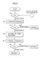
- FIG. 6 is a process flow diagram for describing a mounting process for mounting a semiconductor chip 10.
- the semiconductor chip 10 formed as described hereinabove is then subjected to quality inspection, and supplied to the next process, namely ultrasonic bonding process (steps S1 and S2).
- the circuit substrate 12 (refer to FIG. 2) used in the present embodiment consists of an organic material such as phenol resin, polyester resin, epoxy resin, or polyimide resin having a circuit pattern 13 consisting of a metal such as copper on the surface thereof, and is configured so as to be served as a mother board or an interposer (daughter board) in CSP/BGA.
- This circuit substrate 12 is referred to as an organic substrate for the purpose of description.
- FIG. 2 shows an ultrasonic bonding process for bonding the semiconductor chip 10 to the organic substrate 12.
- the semiconductor chip 10 is vacuum-suction held by means of a tool 16 having a hole 16 that is communicated to a vacuum-suction means not shown in the drawing so as that the bump forming plane is directed downward.
- the tool 16 is connected to an ultrasonic vibration means, and the ultrasonic vibration means vibrates the semiconductor chip 10 that is pressed against the circuit pattern (land) 13 on the organic substrate 12 in the direction shown with arrows in FIG. 2, and the tip end of the second step of the bump 11 is melted with frictional heating and fixed to the wiring pattern 13.
- the character 14 denotes resist that covers the surface of the circuit pattern 13.
- the semiconductor chip 10 is connected to the organic substrate 12 electrically and mechanically with interposition of the bump 11. After bonding inspection, the bonded product is supplied to the next process, namely under fill resin coating process (steps S3 and S4).
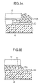
- FIG. 3A and FIG. 3B show under fill resin coating process.
- thermosetting under fill resin 15A is coated on the periphery of the semiconductor chip 10 on the organic substrate 12 (FIG. 3A).
- under fill resin consisting mainly of epoxy resin containing filler is used as the under fill resin 15A.
- the coated resin 15A that has been penetrated into the gap is filled between the semiconductor chip 10 and the organic substrate 12 with aid of capillary phenomenon (FIG. 3B).
- the organic substrate 12 is supplied together with the semiconductor chip into a heating furnace not shown in the drawing, and the resin 15A is thermally hardened (step S5).
- FIG. 5A shows a temperature profile of the heating furnace for thermally hardening the under fill resin 15A filled between the semiconductor chip 10 and the organic substrate 12.
- the under fill resin 15A is heated at first at a temperature T1 that is lower than the hardening temperature of the resin 15A T2 for a predetermined time and then heated at the hardening temperature T2 in the present embodiment.
- An existing heating furnace that is capable to set a heating profile arbitrarily may be used as the heating furnace used in the present embodiment.
- the under fill resin 15A is fluidized the more, penetrates into the gap between the semiconductor chip 10 and the organic substrate 12 deeply and into the narrow areas between bumps 11, and the penetration of the resin 15A into the above-mentioned gaps is improved. Furthermore, the heating at the temperature T1 for a predetermined time prompts the resin molecules to be cross-linked and thermally hardened.
- the temperature gradient during heating is made small to suppress the rapid thermal expansion of the organic substrate 12.
- the stress that acts on the bumps 11 that are served for bonding between the semiconductor chip 10 and the organic substrate 12 is reduced, the bumps 11 are prevented from being damaged or separated during thermal hardening process for hardening the under fill resin 15A, and the bonding reliability is maintained high.
- the resin 15A that has been thermally hardened as described hereinabove mitigates the stress due to mismatching of thermal expansion coefficient between the semiconductor chip 10 and the organic substrate 12 as the under fill coat 15 as shown in FIG. 4, and functions to prevent the stress concentration on the boding portion because the stress is distributed over the whole chip.
- the thermal expansion of the organic substrate 12 due to rapid heating is mitigated in heat treatment for thermal hardening process of under fill resin to prevent the damage (generation of crack) of the bump 11 and separation of the bump 11 effectively.
- the low bonding strength reliability is prevented and the low cost semiconductor device provided with an organic substrate is obtained.
- the ultrasonic bonding method is excellent in productivity in comparison with other bonding methods such as soldering but also the connection resistance (electrical resistance between the bump 11 and the circuit pattern 13) is low. Therefore, the ultrasonic bonding method can be applied to fabricate a semiconductor package such as high frequency device.
Landscapes
- Wire Bonding (AREA)
- Encapsulation Of And Coatings For Semiconductor Or Solid State Devices (AREA)
Abstract
Description
Claims (2)
- A method for manufacturing a semiconductor device, comprising:a bonding process for bonding a semiconductor chip on a circuit substrate constituting of organic material;a resin injection process for injecting and filling thermosetting resin between said bonded circuit substrate and said semiconductor chip; anda thermal hardening process for heating and hardening said filled thermosetting resin at the hardening temperature,wherein said thermal hardening process involves a process for heating at multi-step temperatures for predetermined times respectively between a temperature lower than said thermal hardening temperature and said hardening temperature.
- A method for manufacturing a semiconductor device as claimed in claim 1, wherein said bonding process is ultrasonic bonding process for bonding said semiconductor chip to a circuit pattern on said circuit substrate by means of ultrasonic vibration.
Applications Claiming Priority (2)
| Application Number | Priority Date | Filing Date | Title |
|---|---|---|---|
| JP2000304399A JP2002110715A (en) | 2000-10-04 | 2000-10-04 | Method for manufacturing semiconductor device |
| JP2000304399 | 2000-10-04 |
Publications (2)
| Publication Number | Publication Date |
|---|---|
| EP1195806A2 true EP1195806A2 (en) | 2002-04-10 |
| EP1195806A3 EP1195806A3 (en) | 2002-06-12 |
Family
ID=18785450
Family Applications (1)
| Application Number | Title | Priority Date | Filing Date |
|---|---|---|---|
| EP01123678A Withdrawn EP1195806A3 (en) | 2000-10-04 | 2001-10-02 | Method for underfilling a flip-chip semiconductor device |
Country Status (3)
| Country | Link |
|---|---|
| US (1) | US20020072149A1 (en) |
| EP (1) | EP1195806A3 (en) |
| JP (1) | JP2002110715A (en) |
Cited By (1)
| Publication number | Priority date | Publication date | Assignee | Title |
|---|---|---|---|---|
| US11043524B2 (en) | 2016-11-17 | 2021-06-22 | Olympus Corporation | Device-bonded body, image pickup module, endoscope and method for manufacturing device-bonded body |
Families Citing this family (6)
| Publication number | Priority date | Publication date | Assignee | Title |
|---|---|---|---|---|
| US6855578B2 (en) * | 2002-08-16 | 2005-02-15 | Texas Instruments Incorporated | Vibration-assisted method for underfilling flip-chip electronic devices |
| JP2007305799A (en) * | 2006-05-11 | 2007-11-22 | Fujitsu Ltd | Manufacturing method of semiconductor device |
| CN102315134B (en) * | 2010-07-08 | 2013-05-01 | 技鼎股份有限公司 | Rapid heating and cooling flip chip method |
| CN103985643A (en) * | 2013-02-07 | 2014-08-13 | 中芯国际集成电路制造(上海)有限公司 | Chip mounting process for semiconductor chip packaging process |
| FR3010919A1 (en) * | 2013-09-24 | 2015-03-27 | Univ Rabelais Francois | METHOD FOR DEPOSITING AN INORGANIC MATERIAL ON A SUBSTRATE, IN PARTICULAR TEXTURED AT THE MICRON OR SUBMICRON SCALE |
| CN105047570B (en) * | 2015-06-18 | 2018-03-02 | 苏州奇泰电子有限公司 | A kind of chip BGA package reinforcement means |
Family Cites Families (7)
| Publication number | Priority date | Publication date | Assignee | Title |
|---|---|---|---|---|
| EP0340492A3 (en) * | 1988-05-02 | 1990-07-04 | International Business Machines Corporation | Conformal sealing and interplanar encapsulation of electronic device structures |
| US5121190A (en) * | 1990-03-14 | 1992-06-09 | International Business Machines Corp. | Solder interconnection structure on organic substrates |
| US5471027A (en) * | 1994-07-22 | 1995-11-28 | International Business Machines Corporation | Method for forming chip carrier with a single protective encapsulant |
| US5811317A (en) * | 1995-08-25 | 1998-09-22 | Texas Instruments Incorporated | Process for reflow bonding a semiconductor die to a substrate and the product produced by the product |
| JPH1012669A (en) * | 1996-06-21 | 1998-01-16 | Toshiba Corp | Flip chip connection method |
| US6981317B1 (en) * | 1996-12-27 | 2006-01-03 | Matsushita Electric Industrial Co., Ltd. | Method and device for mounting electronic component on circuit board |
| FR2773642B1 (en) * | 1998-01-13 | 2000-03-03 | Schlumberger Ind Sa | METHOD FOR CONNECTING PLOTS OF A COMPONENT WITH INTEGRATED CIRCUITS TO CONNECTING RANGES OF A PLASTIC SUBSTRATE BY MEANS OF PROTUBERANCES |
-
2000
- 2000-10-04 JP JP2000304399A patent/JP2002110715A/en active Pending
-
2001
- 2001-09-28 US US09/966,942 patent/US20020072149A1/en not_active Abandoned
- 2001-10-02 EP EP01123678A patent/EP1195806A3/en not_active Withdrawn
Cited By (1)
| Publication number | Priority date | Publication date | Assignee | Title |
|---|---|---|---|---|
| US11043524B2 (en) | 2016-11-17 | 2021-06-22 | Olympus Corporation | Device-bonded body, image pickup module, endoscope and method for manufacturing device-bonded body |
Also Published As
| Publication number | Publication date |
|---|---|
| JP2002110715A (en) | 2002-04-12 |
| EP1195806A3 (en) | 2002-06-12 |
| US20020072149A1 (en) | 2002-06-13 |
Similar Documents
| Publication | Publication Date | Title |
|---|---|---|
| JP6408986B2 (en) | BVA interposer | |
| US9263426B2 (en) | PoP structure with electrically insulating material between packages | |
| US6221753B1 (en) | Flip chip technique for chip assembly | |
| US6555917B1 (en) | Semiconductor package having stacked semiconductor chips and method of making the same | |
| US8710651B2 (en) | Semiconductor device and method for manufacturing the same | |
| US8377745B2 (en) | Method of forming a semiconductor device | |
| JP2004260138A (en) | Semiconductor device and manufacturing method thereof | |
| US7598121B2 (en) | Method of manufacturing a semiconductor device | |
| KR20030080032A (en) | Chip scale package with flip chip interconnect | |
| JP2001094003A (en) | Semiconductor device and manufacturing method thereof | |
| US6538335B2 (en) | Semiconductor apparatus and a semiconductor device mounting method | |
| JP2000323624A (en) | Semiconductor device and manufacturing method thereof | |
| US20020089836A1 (en) | Injection molded underfill package and method of assembly | |
| EP1195806A2 (en) | Method for underfilling a flip-chip semiconductor device | |
| US9391031B2 (en) | Method for manufacturing electronic device and electronic device | |
| JPH10154726A (en) | Semiconductor device and manufacturing method thereof | |
| JP3273244B2 (en) | High-density multi-chip module and method for manufacturing the same | |
| JP2006222470A (en) | Semiconductor device and manufacturing method of semiconductor device | |
| JPH10335386A (en) | Semiconductor mounting method | |
| JP2002009111A (en) | Semiconductor flip chip mounting method | |
| JPH11204572A (en) | Semiconductor device mounting structure and method of manufacturing the same | |
| KR101142341B1 (en) | Method for manufacturing of semiconductor package | |
| JP2002299374A (en) | Semiconductor device and manufacturing method thereof | |
| JP2001332584A (en) | Semiconductor device, manufacturing method thereof, substrate and semiconductor chip | |
| JPH11274235A (en) | Semiconductor device and manufacturing method thereof |
Legal Events
| Date | Code | Title | Description |
|---|---|---|---|
| PUAI | Public reference made under article 153(3) epc to a published international application that has entered the european phase |
Free format text: ORIGINAL CODE: 0009012 |
|
| AK | Designated contracting states |
Kind code of ref document: A2 Designated state(s): AT BE CH CY DE DK ES FI FR GB GR IE IT LI LU MC NL PT SE TR |
|
| AX | Request for extension of the european patent |
Free format text: AL;LT;LV;MK;RO;SI |
|
| PUAL | Search report despatched |
Free format text: ORIGINAL CODE: 0009013 |
|
| AK | Designated contracting states |
Kind code of ref document: A3 Designated state(s): AT BE CH CY DE DK ES FI FR GB GR IE IT LI LU MC NL PT SE TR |
|
| AX | Request for extension of the european patent |
Free format text: AL;LT;LV;MK;RO;SI |
|
| 17P | Request for examination filed |
Effective date: 20021112 |
|
| AKX | Designation fees paid |
Designated state(s): DE FR GB |
|
| 17Q | First examination report despatched |
Effective date: 20030214 |
|
| STAA | Information on the status of an ep patent application or granted ep patent |
Free format text: STATUS: THE APPLICATION IS DEEMED TO BE WITHDRAWN |
|
| 18D | Application deemed to be withdrawn |
Effective date: 20030625 |