EP1189288A1 - Dispositif photoelectrique - Google Patents
Dispositif photoelectrique Download PDFInfo
- Publication number
- EP1189288A1 EP1189288A1 EP01908233A EP01908233A EP1189288A1 EP 1189288 A1 EP1189288 A1 EP 1189288A1 EP 01908233 A EP01908233 A EP 01908233A EP 01908233 A EP01908233 A EP 01908233A EP 1189288 A1 EP1189288 A1 EP 1189288A1
- Authority
- EP
- European Patent Office
- Prior art keywords
- photoelectric conversion
- film
- fine particles
- thin film
- transparent conductive
- Prior art date
- Legal status (The legal status is an assumption and is not a legal conclusion. Google has not performed a legal analysis and makes no representation as to the accuracy of the status listed.)
- Granted
Links
- 238000006243 chemical reaction Methods 0.000 claims abstract description 201
- 239000010419 fine particle Substances 0.000 claims abstract description 93
- 239000002245 particle Substances 0.000 claims abstract description 31
- 239000000758 substrate Substances 0.000 claims abstract description 19
- 238000002834 transmittance Methods 0.000 claims abstract description 17
- 239000010408 film Substances 0.000 claims description 197
- 239000010409 thin film Substances 0.000 claims description 84
- 229910021417 amorphous silicon Inorganic materials 0.000 claims description 69
- 229910021419 crystalline silicon Inorganic materials 0.000 claims description 50
- 239000000463 material Substances 0.000 claims description 19
- 239000004065 semiconductor Substances 0.000 claims description 14
- 239000011521 glass Substances 0.000 abstract description 61
- 230000003993 interaction Effects 0.000 abstract description 2
- 239000010410 layer Substances 0.000 description 118
- VYPSYNLAJGMNEJ-UHFFFAOYSA-N Silicium dioxide Chemical compound O=[Si]=O VYPSYNLAJGMNEJ-UHFFFAOYSA-N 0.000 description 61
- 230000000694 effects Effects 0.000 description 27
- 239000000377 silicon dioxide Substances 0.000 description 27
- XOLBLPGZBRYERU-UHFFFAOYSA-N tin dioxide Chemical compound O=[Sn]=O XOLBLPGZBRYERU-UHFFFAOYSA-N 0.000 description 24
- LEVVHYCKPQWKOP-UHFFFAOYSA-N [Si].[Ge] Chemical compound [Si].[Ge] LEVVHYCKPQWKOP-UHFFFAOYSA-N 0.000 description 14
- 239000011230 binding agent Substances 0.000 description 13
- 239000011248 coating agent Substances 0.000 description 11
- 238000000576 coating method Methods 0.000 description 11
- 238000000151 deposition Methods 0.000 description 11
- 229910021424 microcrystalline silicon Inorganic materials 0.000 description 11
- IJGRMHOSHXDMSA-UHFFFAOYSA-N Atomic nitrogen Chemical compound N#N IJGRMHOSHXDMSA-UHFFFAOYSA-N 0.000 description 10
- 229910052710 silicon Inorganic materials 0.000 description 10
- 238000004519 manufacturing process Methods 0.000 description 9
- 239000010703 silicon Substances 0.000 description 9
- 238000005268 plasma chemical vapour deposition Methods 0.000 description 8
- 230000003595 spectral effect Effects 0.000 description 8
- XUIMIQQOPSSXEZ-UHFFFAOYSA-N Silicon Chemical compound [Si] XUIMIQQOPSSXEZ-UHFFFAOYSA-N 0.000 description 7
- 230000008021 deposition Effects 0.000 description 7
- ORUIBWPALBXDOA-UHFFFAOYSA-L magnesium fluoride Chemical group [F-].[F-].[Mg+2] ORUIBWPALBXDOA-UHFFFAOYSA-L 0.000 description 7
- 229910001635 magnesium fluoride Inorganic materials 0.000 description 7
- UQSXHKLRYXJYBZ-UHFFFAOYSA-N Iron oxide Chemical compound [Fe]=O UQSXHKLRYXJYBZ-UHFFFAOYSA-N 0.000 description 6
- BLRPTPMANUNPDV-UHFFFAOYSA-N Silane Chemical compound [SiH4] BLRPTPMANUNPDV-UHFFFAOYSA-N 0.000 description 6
- 229910052681 coesite Inorganic materials 0.000 description 6
- 229910052906 cristobalite Inorganic materials 0.000 description 6
- 239000013078 crystal Substances 0.000 description 6
- 239000007789 gas Substances 0.000 description 6
- 230000006872 improvement Effects 0.000 description 6
- 239000012535 impurity Substances 0.000 description 6
- 229910052682 stishovite Inorganic materials 0.000 description 6
- 229910001887 tin oxide Inorganic materials 0.000 description 6
- 229910052905 tridymite Inorganic materials 0.000 description 6
- QVGXLLKOCUKJST-UHFFFAOYSA-N atomic oxygen Chemical compound [O] QVGXLLKOCUKJST-UHFFFAOYSA-N 0.000 description 5
- 238000000034 method Methods 0.000 description 5
- 239000000203 mixture Substances 0.000 description 5
- 229910052757 nitrogen Inorganic materials 0.000 description 5
- 229910052760 oxygen Inorganic materials 0.000 description 5
- 239000001301 oxygen Substances 0.000 description 5
- 230000004044 response Effects 0.000 description 5
- HBMJWWWQQXIZIP-UHFFFAOYSA-N silicon carbide Chemical compound [Si+]#[C-] HBMJWWWQQXIZIP-UHFFFAOYSA-N 0.000 description 5
- 229910052814 silicon oxide Inorganic materials 0.000 description 5
- 229910000577 Silicon-germanium Inorganic materials 0.000 description 4
- XLOMVQKBTHCTTD-UHFFFAOYSA-N Zinc monoxide Chemical compound [Zn]=O XLOMVQKBTHCTTD-UHFFFAOYSA-N 0.000 description 4
- 150000004703 alkoxides Chemical class 0.000 description 4
- 239000000956 alloy Substances 0.000 description 4
- 125000004429 atom Chemical group 0.000 description 4
- 230000015572 biosynthetic process Effects 0.000 description 4
- 229910052751 metal Inorganic materials 0.000 description 4
- 239000002184 metal Substances 0.000 description 4
- 150000002736 metal compounds Chemical class 0.000 description 4
- 239000000126 substance Substances 0.000 description 4
- 206010034972 Photosensitivity reaction Diseases 0.000 description 3
- 238000010521 absorption reaction Methods 0.000 description 3
- 239000006185 dispersion Substances 0.000 description 3
- 229910052732 germanium Inorganic materials 0.000 description 3
- GNPVGFCGXDBREM-UHFFFAOYSA-N germanium atom Chemical compound [Ge] GNPVGFCGXDBREM-UHFFFAOYSA-N 0.000 description 3
- JEIPFZHSYJVQDO-UHFFFAOYSA-N iron(III) oxide Inorganic materials O=[Fe]O[Fe]=O JEIPFZHSYJVQDO-UHFFFAOYSA-N 0.000 description 3
- 238000005259 measurement Methods 0.000 description 3
- 230000003287 optical effect Effects 0.000 description 3
- 230000036211 photosensitivity Effects 0.000 description 3
- 239000012495 reaction gas Substances 0.000 description 3
- SVTBMSDMJJWYQN-UHFFFAOYSA-N 2-methylpentane-2,4-diol Chemical compound CC(O)CC(C)(C)O SVTBMSDMJJWYQN-UHFFFAOYSA-N 0.000 description 2
- QGZKDVFQNNGYKY-UHFFFAOYSA-N Ammonia Chemical compound N QGZKDVFQNNGYKY-UHFFFAOYSA-N 0.000 description 2
- OKTJSMMVPCPJKN-UHFFFAOYSA-N Carbon Chemical compound [C] OKTJSMMVPCPJKN-UHFFFAOYSA-N 0.000 description 2
- LFQSCWFLJHTTHZ-UHFFFAOYSA-N Ethanol Chemical compound CCO LFQSCWFLJHTTHZ-UHFFFAOYSA-N 0.000 description 2
- YCKRFDGAMUMZLT-UHFFFAOYSA-N Fluorine atom Chemical compound [F] YCKRFDGAMUMZLT-UHFFFAOYSA-N 0.000 description 2
- VEXZGXHMUGYJMC-UHFFFAOYSA-N Hydrochloric acid Chemical compound Cl VEXZGXHMUGYJMC-UHFFFAOYSA-N 0.000 description 2
- UFHFLCQGNIYNRP-UHFFFAOYSA-N Hydrogen Chemical compound [H][H] UFHFLCQGNIYNRP-UHFFFAOYSA-N 0.000 description 2
- ATJFFYVFTNAWJD-UHFFFAOYSA-N Tin Chemical compound [Sn] ATJFFYVFTNAWJD-UHFFFAOYSA-N 0.000 description 2
- GWEVSGVZZGPLCZ-UHFFFAOYSA-N Titan oxide Chemical compound O=[Ti]=O GWEVSGVZZGPLCZ-UHFFFAOYSA-N 0.000 description 2
- 229910052782 aluminium Inorganic materials 0.000 description 2
- 230000005540 biological transmission Effects 0.000 description 2
- 239000005388 borosilicate glass Substances 0.000 description 2
- 229910052799 carbon Inorganic materials 0.000 description 2
- 238000006482 condensation reaction Methods 0.000 description 2
- PKKGKUDPKRTKLJ-UHFFFAOYSA-L dichloro(dimethyl)stannane Chemical compound C[Sn](C)(Cl)Cl PKKGKUDPKRTKLJ-UHFFFAOYSA-L 0.000 description 2
- 230000002349 favourable effect Effects 0.000 description 2
- 239000005329 float glass Substances 0.000 description 2
- 239000011737 fluorine Substances 0.000 description 2
- 229910052731 fluorine Inorganic materials 0.000 description 2
- QUZPNFFHZPRKJD-UHFFFAOYSA-N germane Chemical compound [GeH4] QUZPNFFHZPRKJD-UHFFFAOYSA-N 0.000 description 2
- 229910052986 germanium hydride Inorganic materials 0.000 description 2
- 229910052739 hydrogen Inorganic materials 0.000 description 2
- 239000001257 hydrogen Substances 0.000 description 2
- 230000007062 hydrolysis Effects 0.000 description 2
- 238000006460 hydrolysis reaction Methods 0.000 description 2
- TWNQGVIAIRXVLR-UHFFFAOYSA-N oxo(oxoalumanyloxy)alumane Chemical compound O=[Al]O[Al]=O TWNQGVIAIRXVLR-UHFFFAOYSA-N 0.000 description 2
- BPUBBGLMJRNUCC-UHFFFAOYSA-N oxygen(2-);tantalum(5+) Chemical compound [O-2].[O-2].[O-2].[O-2].[O-2].[Ta+5].[Ta+5] BPUBBGLMJRNUCC-UHFFFAOYSA-N 0.000 description 2
- RVTZCBVAJQQJTK-UHFFFAOYSA-N oxygen(2-);zirconium(4+) Chemical compound [O-2].[O-2].[Zr+4] RVTZCBVAJQQJTK-UHFFFAOYSA-N 0.000 description 2
- 239000011164 primary particle Substances 0.000 description 2
- 229910052711 selenium Inorganic materials 0.000 description 2
- 230000035945 sensitivity Effects 0.000 description 2
- 229910000077 silane Inorganic materials 0.000 description 2
- -1 silicon alkoxide Chemical class 0.000 description 2
- 239000002356 single layer Substances 0.000 description 2
- 229910052717 sulfur Inorganic materials 0.000 description 2
- 229910001936 tantalum oxide Inorganic materials 0.000 description 2
- OGIDPMRJRNCKJF-UHFFFAOYSA-N titanium oxide Inorganic materials [Ti]=O OGIDPMRJRNCKJF-UHFFFAOYSA-N 0.000 description 2
- DTQVDTLACAAQTR-UHFFFAOYSA-N trifluoroacetic acid Substances OC(=O)C(F)(F)F DTQVDTLACAAQTR-UHFFFAOYSA-N 0.000 description 2
- 238000007738 vacuum evaporation Methods 0.000 description 2
- 239000011787 zinc oxide Substances 0.000 description 2
- 229910001928 zirconium oxide Inorganic materials 0.000 description 2
- ZOXJGFHDIHLPTG-UHFFFAOYSA-N Boron Chemical compound [B] ZOXJGFHDIHLPTG-UHFFFAOYSA-N 0.000 description 1
- 229910004613 CdTe Inorganic materials 0.000 description 1
- VGGSQFUCUMXWEO-UHFFFAOYSA-N Ethene Chemical compound C=C VGGSQFUCUMXWEO-UHFFFAOYSA-N 0.000 description 1
- 239000005977 Ethylene Substances 0.000 description 1
- KRHYYFGTRYWZRS-UHFFFAOYSA-N Fluorane Chemical compound F KRHYYFGTRYWZRS-UHFFFAOYSA-N 0.000 description 1
- OAICVXFJPJFONN-UHFFFAOYSA-N Phosphorus Chemical compound [P] OAICVXFJPJFONN-UHFFFAOYSA-N 0.000 description 1
- 229910052581 Si3N4 Inorganic materials 0.000 description 1
- BQCADISMDOOEFD-UHFFFAOYSA-N Silver Chemical compound [Ag] BQCADISMDOOEFD-UHFFFAOYSA-N 0.000 description 1
- 239000004115 Sodium Silicate Substances 0.000 description 1
- BOTDANWDWHJENH-UHFFFAOYSA-N Tetraethyl orthosilicate Chemical compound CCO[Si](OCC)(OCC)OCC BOTDANWDWHJENH-UHFFFAOYSA-N 0.000 description 1
- 238000002441 X-ray diffraction Methods 0.000 description 1
- 230000006978 adaptation Effects 0.000 description 1
- 229910045601 alloy Inorganic materials 0.000 description 1
- XAGFODPZIPBFFR-UHFFFAOYSA-N aluminium Chemical compound [Al] XAGFODPZIPBFFR-UHFFFAOYSA-N 0.000 description 1
- 229910021529 ammonia Inorganic materials 0.000 description 1
- 230000008901 benefit Effects 0.000 description 1
- 229910052796 boron Inorganic materials 0.000 description 1
- YMLFYGFCXGNERH-UHFFFAOYSA-K butyltin trichloride Chemical compound CCCC[Sn](Cl)(Cl)Cl YMLFYGFCXGNERH-UHFFFAOYSA-K 0.000 description 1
- 230000015556 catabolic process Effects 0.000 description 1
- 239000003054 catalyst Substances 0.000 description 1
- 229910000420 cerium oxide Inorganic materials 0.000 description 1
- 238000005229 chemical vapour deposition Methods 0.000 description 1
- 239000008119 colloidal silica Substances 0.000 description 1
- 150000001875 compounds Chemical class 0.000 description 1
- 230000007547 defect Effects 0.000 description 1
- 238000006731 degradation reaction Methods 0.000 description 1
- 238000009792 diffusion process Methods 0.000 description 1
- 230000003292 diminished effect Effects 0.000 description 1
- 238000001035 drying Methods 0.000 description 1
- 238000001704 evaporation Methods 0.000 description 1
- 230000008020 evaporation Effects 0.000 description 1
- 239000005338 frosted glass Substances 0.000 description 1
- 229910021485 fumed silica Inorganic materials 0.000 description 1
- 229910052733 gallium Inorganic materials 0.000 description 1
- 229940051250 hexylene glycol Drugs 0.000 description 1
- 125000004435 hydrogen atom Chemical group [H]* 0.000 description 1
- 229910000040 hydrogen fluoride Inorganic materials 0.000 description 1
- 230000003301 hydrolyzing effect Effects 0.000 description 1
- LQJIDIOGYJAQMF-UHFFFAOYSA-N lambda2-silanylidenetin Chemical compound [Si].[Sn] LQJIDIOGYJAQMF-UHFFFAOYSA-N 0.000 description 1
- 239000002932 luster Substances 0.000 description 1
- 229910044991 metal oxide Inorganic materials 0.000 description 1
- 150000004706 metal oxides Chemical class 0.000 description 1
- 238000002156 mixing Methods 0.000 description 1
- 229910000484 niobium oxide Inorganic materials 0.000 description 1
- URLJKFSTXLNXLG-UHFFFAOYSA-N niobium(5+);oxygen(2-) Chemical compound [O-2].[O-2].[O-2].[O-2].[O-2].[Nb+5].[Nb+5] URLJKFSTXLNXLG-UHFFFAOYSA-N 0.000 description 1
- BMMGVYCKOGBVEV-UHFFFAOYSA-N oxo(oxoceriooxy)cerium Chemical compound [Ce]=O.O=[Ce]=O BMMGVYCKOGBVEV-UHFFFAOYSA-N 0.000 description 1
- 239000003973 paint Substances 0.000 description 1
- 229910052698 phosphorus Inorganic materials 0.000 description 1
- 239000011574 phosphorus Substances 0.000 description 1
- 230000009257 reactivity Effects 0.000 description 1
- 238000001004 secondary ion mass spectrometry Methods 0.000 description 1
- 239000011163 secondary particle Substances 0.000 description 1
- 125000005372 silanol group Chemical group 0.000 description 1
- 229910010271 silicon carbide Inorganic materials 0.000 description 1
- HQVNEWCFYHHQES-UHFFFAOYSA-N silicon nitride Chemical compound N12[Si]34N5[Si]62N3[Si]51N64 HQVNEWCFYHHQES-UHFFFAOYSA-N 0.000 description 1
- 229910052709 silver Inorganic materials 0.000 description 1
- 239000004332 silver Substances 0.000 description 1
- 239000005361 soda-lime glass Substances 0.000 description 1
- NTHWMYGWWRZVTN-UHFFFAOYSA-N sodium silicate Chemical compound [Na+].[Na+].[O-][Si]([O-])=O NTHWMYGWWRZVTN-UHFFFAOYSA-N 0.000 description 1
- 229910052911 sodium silicate Inorganic materials 0.000 description 1
- 238000003980 solgel method Methods 0.000 description 1
- 239000007787 solid Substances 0.000 description 1
- 238000004528 spin coating Methods 0.000 description 1
- 238000004544 sputter deposition Methods 0.000 description 1
- 238000003756 stirring Methods 0.000 description 1
- 229910052715 tantalum Inorganic materials 0.000 description 1
- 238000005979 thermal decomposition reaction Methods 0.000 description 1
- 229910052719 titanium Inorganic materials 0.000 description 1
- 239000010936 titanium Substances 0.000 description 1
- 238000011144 upstream manufacturing Methods 0.000 description 1
- 239000012808 vapor phase Substances 0.000 description 1
- 238000005406 washing Methods 0.000 description 1
- XLYOFNOQVPJJNP-UHFFFAOYSA-N water Chemical compound O XLYOFNOQVPJJNP-UHFFFAOYSA-N 0.000 description 1
- 229910052726 zirconium Inorganic materials 0.000 description 1
Images


Classifications
-
- H—ELECTRICITY
- H01—ELECTRIC ELEMENTS
- H01L—SEMICONDUCTOR DEVICES NOT COVERED BY CLASS H10
- H01L31/00—Semiconductor devices sensitive to infrared radiation, light, electromagnetic radiation of shorter wavelength or corpuscular radiation and specially adapted either for the conversion of the energy of such radiation into electrical energy or for the control of electrical energy by such radiation; Processes or apparatus specially adapted for the manufacture or treatment thereof or of parts thereof; Details thereof
- H01L31/02—Details
- H01L31/0216—Coatings
- H01L31/02161—Coatings for devices characterised by at least one potential jump barrier or surface barrier
- H01L31/02167—Coatings for devices characterised by at least one potential jump barrier or surface barrier for solar cells
- H01L31/02168—Coatings for devices characterised by at least one potential jump barrier or surface barrier for solar cells the coatings being antireflective or having enhancing optical properties for the solar cells
-
- G—PHYSICS
- G02—OPTICS
- G02B—OPTICAL ELEMENTS, SYSTEMS OR APPARATUS
- G02B1/00—Optical elements characterised by the material of which they are made; Optical coatings for optical elements
- G02B1/10—Optical coatings produced by application to, or surface treatment of, optical elements
- G02B1/11—Anti-reflection coatings
- G02B1/111—Anti-reflection coatings using layers comprising organic materials
-
- G—PHYSICS
- G02—OPTICS
- G02B—OPTICAL ELEMENTS, SYSTEMS OR APPARATUS
- G02B1/00—Optical elements characterised by the material of which they are made; Optical coatings for optical elements
- G02B1/10—Optical coatings produced by application to, or surface treatment of, optical elements
- G02B1/11—Anti-reflection coatings
- G02B1/113—Anti-reflection coatings using inorganic layer materials only
- G02B1/115—Multilayers
- G02B1/116—Multilayers including electrically conducting layers
-
- H—ELECTRICITY
- H01—ELECTRIC ELEMENTS
- H01L—SEMICONDUCTOR DEVICES NOT COVERED BY CLASS H10
- H01L31/00—Semiconductor devices sensitive to infrared radiation, light, electromagnetic radiation of shorter wavelength or corpuscular radiation and specially adapted either for the conversion of the energy of such radiation into electrical energy or for the control of electrical energy by such radiation; Processes or apparatus specially adapted for the manufacture or treatment thereof or of parts thereof; Details thereof
- H01L31/02—Details
- H01L31/0216—Coatings
- H01L31/02161—Coatings for devices characterised by at least one potential jump barrier or surface barrier
-
- H—ELECTRICITY
- H01—ELECTRIC ELEMENTS
- H01L—SEMICONDUCTOR DEVICES NOT COVERED BY CLASS H10
- H01L31/00—Semiconductor devices sensitive to infrared radiation, light, electromagnetic radiation of shorter wavelength or corpuscular radiation and specially adapted either for the conversion of the energy of such radiation into electrical energy or for the control of electrical energy by such radiation; Processes or apparatus specially adapted for the manufacture or treatment thereof or of parts thereof; Details thereof
- H01L31/02—Details
- H01L31/0236—Special surface textures
- H01L31/02363—Special surface textures of the semiconductor body itself, e.g. textured active layers
-
- Y—GENERAL TAGGING OF NEW TECHNOLOGICAL DEVELOPMENTS; GENERAL TAGGING OF CROSS-SECTIONAL TECHNOLOGIES SPANNING OVER SEVERAL SECTIONS OF THE IPC; TECHNICAL SUBJECTS COVERED BY FORMER USPC CROSS-REFERENCE ART COLLECTIONS [XRACs] AND DIGESTS
- Y02—TECHNOLOGIES OR APPLICATIONS FOR MITIGATION OR ADAPTATION AGAINST CLIMATE CHANGE
- Y02E—REDUCTION OF GREENHOUSE GAS [GHG] EMISSIONS, RELATED TO ENERGY GENERATION, TRANSMISSION OR DISTRIBUTION
- Y02E10/00—Energy generation through renewable energy sources
- Y02E10/50—Photovoltaic [PV] energy
- Y02E10/547—Monocrystalline silicon PV cells
-
- Y—GENERAL TAGGING OF NEW TECHNOLOGICAL DEVELOPMENTS; GENERAL TAGGING OF CROSS-SECTIONAL TECHNOLOGIES SPANNING OVER SEVERAL SECTIONS OF THE IPC; TECHNICAL SUBJECTS COVERED BY FORMER USPC CROSS-REFERENCE ART COLLECTIONS [XRACs] AND DIGESTS
- Y02—TECHNOLOGIES OR APPLICATIONS FOR MITIGATION OR ADAPTATION AGAINST CLIMATE CHANGE
- Y02E—REDUCTION OF GREENHOUSE GAS [GHG] EMISSIONS, RELATED TO ENERGY GENERATION, TRANSMISSION OR DISTRIBUTION
- Y02E10/00—Energy generation through renewable energy sources
- Y02E10/50—Photovoltaic [PV] energy
- Y02E10/548—Amorphous silicon PV cells
Definitions
- the present invention relates to a photoelectric conversion device. More specifically, the present invention relates to a photoelectric conversion device including a photoelectric conversion layer of semiconductor material that has a relatively small band gap and photosensitivity even in a longer wavelength region.
- a transparent conductive film acting as a transparent electrode, is formed on the glass sheet, and a thin film photoelectric conversion unit including a photoelectric conversion layer is formed on the transparent conductive film.
- a tin oxide film often is employed as the transparent conductive film.
- the unevenness generated on the surface of the transparent conductive film with the growth of crystal grains has the effect of improving photoelectric conversion efficiency by trapping incident light in the photoelectric conversion layer or in the vicinity of the layer (i.e., light trapping effect).
- various surface shapes to improve the photoelectric conversion efficiency have been proposed.
- Examples of the known thin film photoelectric conversion units are as follows: a unit including a photoelectric conversion layer formed of an amorphous silicon thin film, a unit including a photoelectric conversion layer formed of an amorphous silicon germanium thin film, and a unit including a photoelectric conversion layer formed of a crystalline silicon based thin film, such as microcrystalline silicon.
- a tandem-type photoelectric conversion device has been under active development because of its ability to utilize light in a broad wavelength region.
- the tandem-type photoelectric conversion device includes two thin film photoelectric conversion units formed on a transparent conductive film, each unit having a different photoelectric conversion layer.
- a photoelectric conversion device requires some adaptation according to a photoelectric conversion layer to be used.
- the thin film photoelectric conversion unit including the photoelectric conversion layer formed of a crystalline silicon based thin film i.e., a crystalline silicon based thin film photoelectric conversion unit
- the thin film photoelectric conversion unit including the photoelectric conversion layer formed of a crystalline silicon based thin film has a smaller absorption coefficient than that of the amorphous silicon based unit.
- the film thickness is increased simply to increase optical absorption, the manufacturing cost becomes higher. Therefore, the improvement in photoelectric conversion efficiency by taking advantage of the light trapping effect is important particularly to the photoelectric conversion device employing the crystalline silicon based thin film photoelectric conversion unit.
- the unit including the photoelectric conversion layer formed of an amorphous silicon germanium thin film or crystalline silicon based thin film has high sensitivity in the long wavelength region, compared with the unit including the photoelectric conversion layer formed of a general amorphous silicon thin film. Even with the amorphous silicon thin film, however, the spectral response becomes high in the long wavelength region as the film thickness increases. Therefore, when these thin films are used as a photoelectric conversion layer, it is necessary to pay considerable attention to the photoelectric conversion efficiency also in a relatively long wavelength region, e.g., at a wavelength of 650 nm or more.
- a conventional photoelectric conversion device is not always provided with a structure suitable for the characteristics of its photoelectric conversion layer.
- the photoelectric conversion device employing a crystalline silicon based thin film photoelectric conversion unit can have a large light trapping effect when the slope of concave and convex portions in the surface of a transparent conductive film is made sharp. However, this may degrade the quality of a crystalline silicon based thin film to be formed on the transparent conductive film. Even if the crystalline silicon based thin film is formed via other thin films, as in the tandem structure, the surface unevenness with a large degree of slope causes degradation in the crystallinity of the crystalline silicon. Thus, it is desired that the crystalline silicon based thin film-type photoelectric conversion unit should achieve the light trapping effect, which is important to improve the photoelectric conversion efficiency, without relying only on the surface unevenness of the transparent conductive film.
- the conventional photoelectric conversion unit does not always adjust properly the characteristics of other members and thin films to be used with the photoelectric conversion layer, particularly their transmittance and contributions to the light trapping effect in that wavelength region.
- a photoelectric conversion device that includes a photoelectric conversion layer having high photoelectric conversion efficiency even in a relatively long wavelength region, i.e., a photoelectric conversion layer having a relatively small band gap, and that is provided with a structure capable of improving the photoelectric conversion efficiency of the photoelectric conversion layer.
- a photoelectric conversion device that improves the photoelectric conversion efficiency of a crystalline silicon based thin film photoelectric conversion unit without relying only on the light trapping effect obtained by a transparent conductive film.
- a photoelectric conversion device of the present invention includes the following: a transparent substrate having a first principal surface and a second principal surface that are parallel to each other; an antireflection film formed on the first principal surface; a transparent conductive film formed on the second principal surface; at least one photoelectric conversion unit formed on the transparent conductive film; and a back electrode formed on the photoelectric conversion unit.
- the antireflection film contains fine particles with a particle diameter in the range of 0.01 ⁇ m to 1.0 ⁇ m and has an uneven surface derived from the fine particles.
- the transparent substrate has a light transmittance of 75% or more in a wavelength region in the range of 800 nm to 900 nm when measured with the transparent conductive film formed thereon.
- At least one of the photoelectric conversion units includes a thin film of semiconductor material having a band gap of 1.85 eV or less as a photoelectric conversion layer.
- the above photoelectric conversion device has photosensitivity even in a long wavelength region so that an external quantum efficiency at a wavelength of 700 nm is 0.2 or more. It is more preferable that the external quantum efficiency at the same wavelength is 0.3 or more.
- the photoelectric conversion unit including the crystalline silicon based thin film as a photoelectric conversion layer has a thickness of 10 ⁇ m or less.
- a photoelectric conversion device of the present invention can use not only a crystalline silicon based thin film but also an amorphous silicon based thin film as a photoelectric conversion layer.
- the amorphous silicon based thin film include an amorphous silicon thin film, an amorphous silicon germanium thin film, and an amorphous silicon tin thin film.
- the amorphous silicon thin film generally has its peak sensitivity in the wavelength region of 500 to 600 nm, and thus it is not so sensitive to light in a long wavelength region. Therefore, when the amorphous silicon thin film is used as a photoelectric conversion layer, it is preferable that the external quantum efficiency at a wavelength of 700 nm is 0.2 or more.
- the photoelectric conversion device of the present invention is suitable particularly for using a thin film of semiconductor material having a band gap of 1.75 eV or less as a photoelectric conversion layer.
- the band gap of a crystalline silicon thin film is smaller than that of the amorphous silicon thin film, generally about 1.1 eV.
- the thin film photoelectric conversion unit has a thickness of 10 ⁇ m or less, more preferably 5 ⁇ m or less, in order to prevent an excessive increase in the manufacturing cost. There is no particular limitation to the above thickness, and it is preferably 0.1 ⁇ m or more.
- the present invention allows an antireflection film containing fine particles to be formed on the light incident side of a transparent substrate.
- a typical antireflection film for a glass sheet is a magnesium fluoride thin film with a flat surface formed by vacuum evaporation or the like.
- an antireflection film whose surface is made uneven by fine particles is more suitable for the photoelectric conversion layer formed of material with a relatively small band gap, particularly for the photoelectric conversion layer formed of a crystalline silicon thin film with low absorption.
- the antireflection film contributes to the enhancement of the light trapping effect.
- the antireflection film has the effect of reducing reflection in a broad wavelength region, particularly in a long wavelength region, thereby improving the characteristics of a photoelectric conversion device.
- the transmittance of a transparent substrate on which a transparent conductive film is formed exerts a greater influence on the efficiency.
- the transparent substrate with a transparent conductive film has a light transmittance of 75% or more in the wavelength region of 800 to 900 nm.
- Such high light transmittance in the above wavelength region combines the effects of reducing reflection and trapping light by the antireflection film, particularly the light trapping effect, with the improvement in photoelectric conversion efficiency.
- the light trapping effect resulting from the surface shape of the antireflection film is produced in the area including the transparent substrate with a transparent conductive film (i.e., the area from the surface of the antireflection film to a back electrode) in a photoelectric conversion device. Therefore, the amount of light passing through the transparent substrate with a transparent conductive film is increased with the light trapping effect. Thus, the increased amount of light through the transparent substrate with a transparent conductive film reinforces the light trapping effect obtained by the antireflection film.
- a combination of the above thin film photoelectric conversion unit, antireflection film, and glass sheet with a transparent conductive film can improve the photoelectric conversion efficiency rationally while preventing unnecessary increase in the manufacturing cost.
- FIG. 1 is a cross-sectional view of a preferred embodiment of a photoelectric conversion device of the present invention.
- the photoelectric conversion device has a tandem structure, in which an antireflection film 1, a glass sheet 2, an underlying film 3, a transparent conductive film 4, an amorphous silicon based thin film photoelectric conversion unit 5, a crystalline silicon based thin film photoelectric conversion unit 6, and a back electrode 7 are stacked in this order from the light incident side.
- the antireflection film 1 of the photoelectric conversion device has an uneven surface derived from the shapes of fine particles.
- the antireflection film 1 contains fine particles and a binder.
- oxide fine particles are preferable, and fine particles made of material having a refractive index of 2.0 or less, particularly 1.6 or less, are preferable.
- the particularly suitable oxide fine particles are silica fine particles.
- fine particles including silicon oxide as the main component are referred to as silica fine particles, even if they include other minor components.
- Examples of silica fine particles include the following: silica fine particles synthesized by the reaction of silicon alkoxide in the presence of a basic catalyst, such as ammonia, with a sol-gel process, colloidal silica of sodium silicate or the like, and fumed silica synthesized in a vapor phase.
- the antireflection film having the exposed fine particles on the surface has a remarkable effect of improving the photoelectric conversion efficiency.
- the antireflection film formed of fine particles has gaps between the fine particles.
- the inclusion of gaps reduces a substantial refractive index of the film and improves the antireflection effect.
- the structure of the antireflection film changes depending on the particle size of the fine particles.
- the gaps between particles decrease as the particle size of the fine particles is diminished. Consequently, capillary force is increased to allow moisture and organic matters in the air to enter the gaps gradually.
- the gaps disappear, a refractive index of the film is increased.
- the adhesion to a glass sheet is lowered with increasing particle size of the fine particles. In view of this, it is preferable that the fine particles have an average particle diameter of 0.01 ⁇ m to 1.0 ⁇ m.
- the particle size of the fine particles also can be used to adjust the optical characteristics of the antireflection film.
- the particle diameter suitable for the enhancement of antireflection effect is in the range of 0.05 ⁇ m to 0.15 ⁇ m.
- an antireflection effect is obtained that exceeds a magnesium fluoride film in a broad wavelength region, the magnesium fluoride film with an appropriate thickness being formed by vacuum evaporation.
- the fine particles with a particle diameter of 0.2 ⁇ m to 0.8 ⁇ m have been found to improve the light trapping effect significantly as well.
- a part of the surface of a glass sheet is coated with silica fine particles having a particle size within the above range, that alone leads to the improvement in the photoelectric conversion efficiency of a unit including a photoelectric conversion layer whose peak spectral response is shifted relatively to the long wavelength region, such as a crystalline silicon thin film.
- the fine particles described above may interact strongly with light in the wavelength region of 600 to 1000 nm and contribute largely to trapping light in the wavelength region where the spectral response of a crystalline silicon based photoelectric conversion layer or the like is high.
- the fine particles have an average particle diameter of about 0.05 ⁇ m to 0.8 ⁇ m.
- unevenness derived from the fine particles is formed in the area of at least 60% of the principal surface of a glass sheet.
- a large antireflection effect can be obtained when the fine particles having a particle diameter of 0.05 ⁇ m to 0.15 ⁇ m occupy at least 50% of the uneven area derived from the fine particles.
- a large light trapping effect in the wavelength region where the spectral response of a crystalline silicon based photoelectric conversion layer is high can be obtained when the fine particles having a particle diameter of 0.2 ⁇ m to 0.8 ⁇ m occupy at least 30% of the uneven area derived from the fine particles.
- the presence of both fine particles together on the surface with the above percentage provides especially preferable results.
- the particle size of fine particles can be evaluated roughly with a scanning electron microscope. For precise measurements, a transmission electron microscope can be used.
- the particle size of individual particles (primary particles) instead of aggregated particles (e.g., secondary particles linked in a chain form) is employed.
- the antireflection film includes a binder as well as fine particles.
- the binder serves to bind the fine particles together and provide adhesion between the fine particles and a glass sheet.
- the binder is at least one metal oxide selected from the group consisting of silicon oxide, aluminum oxide, titanium oxide, zirconium oxide, and tantalum oxide.
- the binder material is at least one alkoxide of metal selected from Si, Al, Ti, Zr, and Ta.
- the refractive index of the binder components affects reflectance. Therefore, silicon alkoxide having a small refractive index, particularly silicon tetraalkoxide or its oligomer, is preferable.
- the method for manufacturing an antireflection film containing silica fine particles and a binder is described in more detail below.
- the antireflection film can be formed with a coating solution that is prepared using silica fine particles and a metal compound such as metal alkoxide.
- the coating solution may be prepared by mixing a hydrolyzate of the metal compound and the silica fine particles.
- the coating solution is prepared by hydrolyzing a hydrolyzable metal compound in the presence of the silica fine particles.
- the hydrolysis of metal alkoxide in the presence of the silica fine particles accelerates a condensation reaction between a silanol group on the silica fine particle surface and the metal alkoxide in the coating solution.
- the condensation reaction enhances the adhesion between the silica fine particles. In addition, it reinforces the adhesion of the fine particles to a glass substrate by increasing reactivity of the silica fine particle surface.
- the coating solution thus prepared is applied to a glass sheet and then heated, resulting in an antireflection film formed on the glass sheet.
- An antireflection film with a high area ratio of unevenness derived from silica fine particles can be formed in the following manner: the hydrolysis of a metal compound that acts as a binder is promoted in the presence of the silica fine particles or the content of binder is set to be within an appropriate range (e.g., the weight ratio of the binder is not more than that of the silica fine particles).
- the amount of binder there is no particular limitation to the amount of binder, as long as the antireflection film has an uneven surface derived from the shapes of the fine particles.
- the glass sheet 2 is not limited particularly by composition and thickness, as long as it has a light transmittance of 75% or more in the wavelength region of 800 to 900 nm with a transparent conductive film formed thereon.
- the above light transmittance can be obtained easily when the glass has such a composition that the total amount of iron oxide, expressed by weight percentage in terms of Fe 2 O 3 , is 0.1% or less, preferably 0.08% or less.
- the glass sheet with a transparent conductive film has a light transmittance of 80% or more in the wavelength region of 500 to 600 nm.
- an antireflection film is formed on the bottom surface of the glass sheet (i.e., the surface in contact with the molten tin in a float bath). Since the bottom surface is superior to the opposite top surface in flatness, it is suitable for the application of a coating solution containing fine particles.
- an ITO film or zinc oxide film may be used.
- a film including tin oxide as the main component specifically a tin oxide film doped with impurities such as fluorine to increase conductivity.
- the thickness of the transparent conductive film can be determined properly by conductivity required in accordance with a photoelectric conversion unit to be used and its desired photoelectric conversion efficiency. Considering the necessity to set the light transmittance of the glass sheet with a transparent conductive film within the above range, a suitable thickness of the transparent conductive film ranges from about 400 nm to 1000 nm.
- the surface unevenness of the transparent conductive film formed by the growth of crystal grains or the like further improves the light trapping effect.
- the formation of unevenness in the transparent conductive film surface is not essential in this embodiment. If the unevenness of this film is excessively sharp, the quality of a crystalline silicon based thin film may be degraded.
- the transparent conductive film has a haze ratio of 20% or less, particularly when a crystalline silicon based thin film is used.
- the underlying film 3 is often provided to prevent the diffusion of alkaline component from a glass sheet and to adjust the optical characteristics of the glass sheet with a transparent conductive film.
- the underlying film is formed so that the glass sheet with a transparent conductive film has a light transmittance of 75% or more in the wavelength region of 800 to 900 nm with the underlying film interposed between the glass sheet and the transparent conductive film.
- the underlying film may be composed of a single layer or plurality of layers.
- a preferred example of the underlying film is a film having a two-layer structure that includes a high refractive index film and a low refractive index film in this order from the glass sheet side.
- the high refractive index film is formed of at least one selected from tin oxide, titanium oxide, zinc oxide, tantalum oxide, niobium oxide, cerium oxide, zirconium oxide, silicon nitride, silicon oxynitride (SiON), and a mixture of these substances. It is preferable that this film has a thickness of 5 nm to 100 nm and a refractive index of 1.7 to 2.7.
- the low refractive index film having a refractive index relatively lower than that of the high refractive index film, is formed of at least one selected from silicon oxide, aluminum oxide, silicon oxide containing carbon (SiOC), and a mixture of these substances. It is preferable that this film has a thickness of 1 nm to 60 nm and a refractive index of 1.4 to 1.8.
- a method for forming the underlying film and the transparent conductive film there is no particular limitation on a method for forming the underlying film and the transparent conductive film, and a method that includes thermal decomposition of a material for producing a film on a glass sheet or glass ribbon in the glass sheet production line, particularly a CVD method, is preferable.
- the photoelectric conversion unit preferably includes a plurality of layers, though a single layer may be used.
- the photoelectric conversion device in FIG. 1 has a so-called tandem structure, in which the unit including the photoelectric conversion layer formed of an amorphous silicon based thin film (i.e., an amorphous silicon based thin film photoelectric conversion unit) 5 and the unit including the photoelectric conversion layer formed of a crystalline silicon based thin film (i.e., a crystalline silicon based thin film photoelectric conversion unit) 6 are stacked in this order from the glass sheet side.
- an amorphous silicon based thin film i.e., an amorphous silicon based thin film photoelectric conversion unit
- a crystalline silicon based thin film i.e., a crystalline silicon based thin film photoelectric conversion unit
- the photoelectric conversion device in FIG. 1 can achieve effective utilization of light in a broad wavelength region by using the photoelectric conversion layer formed of a crystalline silicon based thin film having a relatively small band gap (about 1.1 eV) with that formed of an amorphous silicon based thin film having a relatively large band gap.
- the photoelectric conversion device of the present invention is not limited to the structure shown in FIG. 1.
- crystalline silicon is used as a material with a small band gap ( ⁇ 1.85 eV) in this structure.
- a semiconductor material having a band gap of 1.85 eV or less is not limited to the crystalline silicon.
- the amorphous silicon based thin film photoelectric conversion unit is formed by depositing each of the p-type, i-type, and n-type semiconductor layers in this order by plasma CVD.
- the semiconductor layers may be deposited in the following order: a p-type microcrystalline silicon based layer doped with at least 0.01 at% boron that is an impurity atom for determining the conduction type, an intrinsic amorphous silicon layer that acts as a photoelectric conversion portion, and an n-type microcrystalline silicon based layer doped with at least 0.01 at% phosphorus that is an impurity atom for determining the conduction type.
- each of the semiconductor layers is not limited to that described above.
- the impurity atom in the p-type microcrystalline silicon based layer may be aluminum or the like, and an amorphous silicon based layer may be used as the p-layer.
- the p-layer can be formed of alloy material such as amorphous or microcrystalline silicon carbide and silicon germanium.
- the suitable thickness of the amorphous silicon based thin film photoelectric conversion unit is 0.5 ⁇ m or less.
- the conduction type (p-type and n-type) microcrystalline silicon based layers each have a thickness of 3 nm to 100 nm, more preferably 5 nm to 50 nm.
- the intrinsic amorphous silicon layer is formed by plasma CVD with the temperature of an underlying layer maintained at 450°C or less.
- This layer is formed as a substantially intrinsic semiconductor thin film that includes impurity atoms for determining the conduction type with a density of 1 ⁇ 1018 cm -3 or less.
- the generally preferred thickness of the intrinsic amorphous silicon layer though it depends on the configuration of a photoelectric conversion device, ranges from 0.05 ⁇ m to 0.5 ⁇ m.
- the amorphous silicon based thin film photoelectric conversion unit can use a layer of alloy material instead of the intrinsic amorphous silicon layer.
- Such a layer examples include an amorphous silicon carbide layer (e.g., the amorphous silicon carbide layer of amorphous silicon containing not more than 10 at% carbon) and an amorphous silicon germanium layer (e.g., the amorphous silicon germanium layer of amorphous silicon containing not more than 30 at% germanium).
- an amorphous silicon carbide layer e.g., the amorphous silicon carbide layer of amorphous silicon containing not more than 10 at% carbon
- an amorphous silicon germanium layer e.g., the amorphous silicon germanium layer of amorphous silicon containing not more than 30 at% germanium.
- the intrinsic amorphous silicon layer whose thickness is increased to the extent that the external quantum efficiency at a wavelength of 700 nm is 0.2 or more is used as a photoelectric conversion layer.
- the photoelectric conversion layer may be formed of an amorphous silicon alloy based material to which germanium or the like is added so as to increase the external quantum efficiency to the above extent.
- the crystalline silicon based thin film photoelectric conversion unit also is formed by depositing each of the pin-type semiconductor layers in this order by plasma CVD, following the same procedure as that for the amorphous silicon based thin film photoelectric conversion unit.
- a crystalline silicon based photoelectric conversion layer acting as the photoelectric conversion layer (i-layer) in the crystalline silicon based thin film photoelectric conversion unit, is formed by plasma CVD with the temperature of an underlying layer maintained at 450°C or less.
- crystalline silicon based photoelectric conversion layer As the crystalline silicon based photoelectric conversion layer, a non-doped intrinsic silicon polycrystalline thin film, a microcrystalline silicon thin film with a crystalline volume fraction of at least 80%, a weak p-type or n-type silicon based thin film containing a trace amount of impurities but having a sufficient photoelectric conversion function, or the like can be used. Moreover, layers of alloy material such as silicon carbide and silicon germanium may be used.
- the crystalline silicon based photoelectric conversion layer has a thickness of 0.1 ⁇ m to 10 ⁇ m, more preferably 5 ⁇ m or less.
- the photoelectric conversion layer formed at low temperatures of 450°C or less contains a relatively large amount of hydrogen atoms to terminate or deactivate defects in and between crystal grains. It is preferable that the hydrogen content in the layer ranges from 0.5 to 30 at%, more preferably 1 to 20 at%.
- crystal grains in the crystalline silicon based photoelectric conversion layer grow in the thickness direction from an underlying layer to form columns. It is preferable that most crystal grains have (110) preferred orientation planes parallel to the film surface.
- the crystalline silicon based thin film photoelectric conversion unit Compared with the amorphous silicon based thin film photoelectric conversion unit, the crystalline silicon based thin film photoelectric conversion unit generates a low open-circuit voltage and has a high short-circuit current density. Therefore, light transmittance contributes more to the photoelectric conversion efficiency than the sheet resistance of a conductive film on a glass sheet. Accordingly, providing the antireflection film having an uneven surface derived from fine particles and the glass sheet with a transparent conductive film having an improved light transmittance increases the amount of incident light and enables effective trapping of the incident light, which leads to a significant improvement in the photoelectric conversion efficiency.
- the amorphous silicon photoelectric conversion layer has its maximum spectral response in the wavelength region of about 500 to 600 nm.
- the crystalline silicon photoelectric conversion layer has a maximum in the range of about 700 to 900 nm.
- the antireflection film containing fine particles with a particle diameter of 0.05 ⁇ m to 0.15 ⁇ m and those with a particle diameter of 0.2 ⁇ m to 0.8 ⁇ m, both fine particles being exposed on the surface is suitable particularly for a tandem-type photoelectric conversion device including the above two photoelectric conversion layers.
- a "crystalline” material in this embodiment includes a material having a crystalline volume fraction of at least 50%, even if the material is locally amorphous.
- a "silicon based” material includes a semiconductor material containing at least 50 at% silicon, such as amorphous silicon germanium, in addition to amorphous or crystalline silicon.
- the present invention can be applied to a photoelectric conversion device including a thin film of compound semiconductor (e.g., CdTe, CuIn(S, Se) 2 , and Cu(In, Ga)(S, Se) 2 ) as the photoelectric conversion layer.
- compound semiconductor e.g., CdTe, CuIn(S, Se) 2 , and Cu(In, Ga)(S, Se) 2
- a tin oxide film (SnO 2 film), a silicon oxide film (SiO 2 film), and a fluorine-containing tin oxide film (SnO 2 :F film) were formed in this order on a glass ribbon using a plurality of coaters arranged in a float bath.
- the glass ribbon is formed to have a thickness of 4 mm and the total amount of iron oxide of 0.01 wt% in terms of Fe 2 O 3 .
- the glass ribbon had a temperature of about 650°C immediately before reaching a coater located at the furthest upstream position, and a mixed gas of dimethyltin dichloride (vapor), oxygen and nitrogen was supplied from the coater, so that a SnO 2 film having a thickness of 25 nm was formed on the glass ribbon. Then, a mixed gas of monosilane, ethylene, oxygen and nitrogen was supplied from a coater located downstream from said coater, and a SiO 2 film having a thickness of 25 nm was formed on the SnO 2 film.
- vapor dimethyltin dichloride
- Example 1 a mixed gas of dimethyltin dichloride (vapor), oxygen, nitrogen and hydrogen fluoride (vapor) was supplied from a coater located further downstream from said coater, and a SnO 2 :F film having a thickness of 500 nm was formed on the SiO 2 film.
- the glass ribbon was cut into a predetermined size, resulting in a glass sheet with a transparent conductive film (hereinafter, referred to as "Sample 1").
- a SiO 2 film and a SnO 2 :F film were formed in this order on a borosilicate glass sheet having a thickness of 0.7 mm.
- the glass sheet that was cut into a predetermined size beforehand was heated to about 600°C, and a mixed gas of monosilane, oxygen and nitrogen was supplied to the surface of the glass sheet to form a SiO 2 film having a thickness of 25 nm. Then, a mixed gas of monobutyltin trichloride (vapor), oxygen, water vapor, nitrogen and trifluoroacetic acid (vapor) was supplied, and a SnO 2 :F film having a thickness of 600 nm was formed on the SiO 2 film.
- a glass sheet with a transparent conductive film hereinafter, referred to as "Sample 2" was obtained.
- Example 3 A glass sheet with a transparent conductive film (hereinafter, referred to as "Sample 3") was obtained in the same manner as that for Sample 1, except that the total amount of iron oxide in the glass ribbon was 0.11 wt% in terms of Fe 2 O 3 and the thickness of the SnO 2 :F film was 800 nm.
- the glass sheet with a transparent conductive film obtained in the above was washed, dried, and then an antireflection film was formed on the opposite surface of the glass sheet to the transparent conductive film.
- a dispersion of silica fine particles having a predetermined average primary particle size (manufactured by Nippon Shokubai Co., Ltd.) was added ethanol, tetraethoxysilane, and concentrated hydrochloric acid successively while stirring the dispersion, which then was stirred further to cause a reaction.
- the mixture was diluted with hexylene glycol to give a coating solution.
- the coating solution was applied to the surface of the glass sheet by spin coating, and the glass sheet was placed in an electric furnace at 700°C for 2 minutes to form an antireflection film.
- the silica fine particle dispersions with different average particle sizes were mixed at a predetermined ratio of the solid matter.
- the glass sheet with a transparent conductive film obtained in the above was washed, dried, and then a magnesium fluoride film having a thickness of 100 nm was formed on the opposite surface of the glass sheet to the transparent conductive film by EB evaporation, which results in an antireflection film.
- the film deposition temperature was set to a room temperature and the film deposition rate was 1 nm/sec.
- the surfaces of the antireflection films of Samples 4 to 11 were observed with a scanning electron microscope to measure the ratio of the area of the glass surface coated with silica fine particles (i.e., a coating ratio). When those samples included silica fine particles having different average particle sizes, further measurement was made to determine the ratio of the area occupied by each of the fine particles to the area coated with the fine particles. Table 2 shows the results.
- FIGS. 2 to 4 show the results of scanning electron microscope observation of Samples 4 to 6, respectively. These results indicated that the fine particles to form the respective antireflection films were substantially spherical in shape and the variation in particle diameter was rather small. In each sample, substantially all the fine particles A have a particle diameter of 0.05 to 0.15 ⁇ m and substantially all the fine particles B have a particle diameter of 0.2 to 0.8 ⁇ m.
- an amorphous silicon thin film photoelectric conversion unit and a crystalline silicon thin film photoelectric conversion unit were formed in this order on the transparent conductive film by plasma CVD.
- the amorphous silicon photoelectric conversion unit included a pin junction where a p-type amorphous silicon carbide layer had a thickness of 15 nm and an n-type amorphous silicon layer had a thickness of 30 nm.
- An intrinsic amorphous silicon layer was formed by RF plasma CVD.
- the film deposition conditions were such that silane (SiH 4 ) was used as a reaction gas, a pressure in the reaction chamber was about 40 Pa, an RF power density was 15 mW/cm 2 , and a film deposition temperature was 150°C.
- An intrinsic amorphous silicon film which was deposited directly on the glass substrate to have a thickness of 300 nm under the same conditions as those described above, had a dark conductivity of 5 ⁇ 10 -10 S/cm.
- the intrinsic amorphous silicon layer had a thickness of 150 nm.
- the intrinsic amorphous silicon layer prepared in the same manner as that described above had a band gap of about 1.75 eV.
- the crystalline silicon thin film photoelectric conversion unit was prepared by depositing a boron-doped p-type microcrystalline silicon based layer, a non-doped intrinsic crystalline silicon layer, and a phosphorus-doped n-type microcrystalline silicon based layer in this order on the n-type amorphous silicon layer.
- the crystalline silicon thin film photoelectric conversion unit had a thickness of 1.5 ⁇ m.
- the thickness of the p-type microcrystalline silicon based layer was 15 nm and that of the n-type microcrystalline silicon based layer was 30 nm.
- the intrinsic crystalline silicon layer prepared in the same manner as that described above had a band gap of about 1.1 eV.
- the intrinsic crystalline silicon layer was formed by plasma CVD under the condition that silane was used as a reaction gas, a pressure in the reaction chamber was about 670 Pa, an RF power density was 150 mW/cm 2 , and a film deposition temperature was 350°C.
- the measurement with a secondary ion mass spectrometry showed that the intrinsic crystalline silicon layer contained 2 at% hydrogen.
- the crystal grains in this layer had (110) planes as preferred orientation planes in the direction parallel to the film surface.
- a back electrode was formed by depositing an ITO layer (with a thickness of 80 nm) and a silver layer (with a thickness of 300 nm) in this order by sputtering, thus providing a photoelectric conversion device.
- the wavelength dependence of external quantum efficiency in each photoelectric conversion device was measured.
- the resultant efficiency for each wavelength was multiplied by the amount of incident light to give an external quantum efficiency, which then was integrated over the entire wavelength, so that the total current was calculated.
- Table 3 shows the results.
- Samples 13 to 16 and 20 had more favorable characteristics than Samples 22 and 21.
- Each of Samples 13 to 16 and 20 used Sample 2 on which an antireflection film was formed with fine particles exposed on the film surface, while Sample 22 used Sample 2 without forming the antireflection film and Sample 21 used Sample 2 on which a magnesium fluoride film was formed.
- Samples 17 and 19, each using Sample 1 on which an antireflection film was formed with fine particles exposed on the film surface also had more favorable characteristics than Sample 23, using Sample 1 without forming the antireflection film.
- Sample 18, which included the glass sheet with a transparent conductive film of low transmittance was degraded significantly in its characteristics.
- FIG. 5 shows the wavelength dependence of external quantum efficiency of Sample 13 (fine particle film), Sample 14 (fine particle mixed film) and Sample 22 (without an antireflection film), respectively.
- the external quantum efficiency was increased in a broad wavelength region.
- using Sample 14 (fine particle mixed film) with the addition of fine particles B improved the external quantum efficiency in the wavelength region of 800 to 900 nm.
- Sample 21 using magnesium fluoride as the antireflection film, had increased external quantum efficiency in the wavelength region near 500 to 600 nm. However, the degree of increase is small compared with the antireflection film containing fine particles, and the external quantum efficiency was hardly increased in the wavelength region near 800 to 900 nm.
- samples were prepared in such a manner that the same film as the antireflection film used in Samples 13, 14, and 21 was formed on a borosilicate glass sheet having a thickness of 0.7 mm.
- the opposite surface of the glass sheet to the film was ground with a grindstone to be in a frosted glass form, which then was coated with a black paint to remove the luster. Consequently, reflection from this surface was suppressed to the extent that it was substantially negligible.
- the spectral reflection characteristics of the antireflection film surface of each sample were measured.
- FIG. 6 shows the results.
- the fine particle film with an average particle diameter of 0.1 ⁇ m was superior to the magnesium fluoride film in antireflection effect in a broad wavelength region.
- the fine particle mixed film in which the fine particles having an average particle diameter of 0.1 ⁇ m were mixed with those having an average particle diameter of 0.3 ⁇ m, was inferior to the fine particle film in antireflection effect.
- the use of the fine particle mixed film improved the external quantum efficiency in the wavelength region near 800 to 900 nm, as shown in FIG. 5. Such improvement in the efficiency was due to the light trapping effect in that wavelength region.
- a photoelectric conversion device including an amorphous silicon based thin film photoelectric conversion unit having the photoelectric conversion layer formed of an amorphous silicon layer with an increased thickness or amorphous silicon germanium layer.
- Sample 4, 5, or 2 was used as the glass sheet with a transparent conductive film so as to correspond to the samples whose external quantum efficiencies were shown in FIG. 5 (i.e., Sample 13 (fine particle film), Sample 14 (fine particle mixed film), and Sample 22 (without an antireflection film)).
- the photoelectric conversion unit including an amorphous silicon layer as the photoelectric conversion layer was prepared in the same manner as that for the amorphous silicon photoelectric conversion unit in a tandem type. However, the thickness of an intrinsic amorphous silicon layer was 320 nm. The intrinsic amorphous silicon layer prepared in the same manner as that described above had a band gap of 1.75 eV.
- the photoelectric conversion unit including an amorphous silicon germanium layer as the photoelectric conversion layer
- p-type and n-type layers were formed in the same manner as that for the amorphous silicon photoelectric conversion unit in a tandem type.
- the photoelectric conversion layer was formed by RF plasma CVD under the condition that SiH 4 and GeH 4 were used as a reaction gas, a pressure in the reaction chamber was about 40 Pa, an RF power density was 15 mW/cm 2 , and a film deposition temperature was 150°C.
- the ratio of GeH 4 to the entire film deposition gas was about 5 mol%.
- the thickness of an intrinsic silicon germanium layer was 200 nm.
- the intrinsic silicon germanium layer prepared in the same manner as that described above had a band gap of 1.55 eV.
- a back electrode was formed on each of the photoelectric conversion units in the same manner as that described above to complete a photoelectric conversion device.
- the wavelength dependence of external quantum efficiency of each photoelectric conversion device was measured in the same manner as that described above.
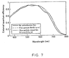
- FIG. 7 shows the wavelength dependence of external quantum efficiency in using the photoelectric conversion unit having the photoelectric conversion layer formed of an amorphous silicon layer with an increased thickness.
- FIG. 8 shows the wavelength dependence of external quantum efficiency in using the photoelectric conversion unit having the photoelectric conversion layer formed of an amorphous silicon germanium layer.
- the intrinsic amorphous silicon thin film was formed to have a thickness of at least about 320 nm, though the degree of increase in the thickness depended on a manufacturing method or the like.
- the external quantum efficiency was improved in a relatively broad wavelength region, including a long wavelength region, by the antireflection films containing fine particles.
- Such antireflection films were suitable for a photoelectric conversion device whose external quantum efficiency was 0.2 or more at a wavelength of 700 nm when including no antireflection film, particularly 0.3 or more.
- the present invention can provide a photoelectric conversion device that improves the photoelectric conversion efficiency with the interaction between a transparent substrate with a transparent conductive film, an antireflection film formed of fine particles, and a photoelectric conversion unit (in particular, a crystalline silicon based photoelectric conversion unit).
- a photoelectric conversion unit in particular, a crystalline silicon based photoelectric conversion unit.
Applications Claiming Priority (5)
| Application Number | Priority Date | Filing Date | Title |
|---|---|---|---|
| JP2000057771 | 2000-03-02 | ||
| JP2000057771 | 2000-03-02 | ||
| JP2000116688 | 2000-04-18 | ||
| JP2000116688A JP2001320067A (ja) | 2000-03-02 | 2000-04-18 | 光電変換装置 |
| PCT/JP2001/001604 WO2001065612A1 (fr) | 2000-03-02 | 2001-03-02 | Dispositif photoelectrique |
Publications (3)
| Publication Number | Publication Date |
|---|---|
| EP1189288A1 true EP1189288A1 (fr) | 2002-03-20 |
| EP1189288A4 EP1189288A4 (fr) | 2005-09-21 |
| EP1189288B1 EP1189288B1 (fr) | 2011-07-20 |
Family
ID=26586657
Family Applications (1)
| Application Number | Title | Priority Date | Filing Date |
|---|---|---|---|
| EP01908233A Expired - Lifetime EP1189288B1 (fr) | 2000-03-02 | 2001-03-02 | Dispositif de conversion photoelectrique |
Country Status (5)
| Country | Link |
|---|---|
| US (1) | US6734352B2 (fr) |
| EP (1) | EP1189288B1 (fr) |
| JP (1) | JP2001320067A (fr) |
| AU (1) | AU3604401A (fr) |
| WO (1) | WO2001065612A1 (fr) |
Cited By (6)
| Publication number | Priority date | Publication date | Assignee | Title |
|---|---|---|---|---|
| DE102006031300A1 (de) * | 2006-06-29 | 2008-01-03 | Schmid Technology Systems Gmbh | Verfahren zur Dotierung von Siliziummaterial für Solarzellen, entsprechend dotiertes Siliziummaterial und Solarzelle |
| WO2008141158A2 (fr) * | 2007-05-10 | 2008-11-20 | Board Of Regents, The University Of Texas System | Structures de surface de substrat et procédés pour former celles-ci |
| CN101295738B (zh) * | 2008-04-15 | 2010-06-02 | 福建钧石能源有限公司 | 膜层及其制造方法和具有该膜层的太阳能电池 |
| WO2012047422A1 (fr) * | 2010-10-06 | 2012-04-12 | 3M Innovative Properties Company | Articles antireflet présentant des revêtements à base de nanosilice |
| WO2012066009A3 (fr) * | 2010-11-16 | 2012-11-15 | Schott Solar Ag | Plaque de verre destinée à la fabrication d'un module solaire à couche mince |
| US20130333752A1 (en) * | 2009-12-21 | 2013-12-19 | Ppg Industries Ohio, Inc. | Photovoltaic Solar Cell With High-Haze Substrate |
Families Citing this family (32)
| Publication number | Priority date | Publication date | Assignee | Title |
|---|---|---|---|---|
| EP1167313B1 (fr) * | 1999-12-13 | 2015-09-23 | Nippon Sheet Glass Co., Ltd. | Article en verre a faible reflexion |
| JP4201259B2 (ja) * | 2002-08-22 | 2008-12-24 | 日東電工株式会社 | 被膜シートの製造方法 |
| US7535019B1 (en) | 2003-02-18 | 2009-05-19 | Nanosolar, Inc. | Optoelectronic fiber |
| JP4713819B2 (ja) * | 2003-04-07 | 2011-06-29 | 株式会社カネカ | 薄膜光電変換装置用基板及びそれを用いた薄膜光電変換装置 |
| JP2005050905A (ja) * | 2003-07-30 | 2005-02-24 | Sharp Corp | シリコン薄膜太陽電池の製造方法 |
| US7994420B2 (en) * | 2004-07-07 | 2011-08-09 | Saint-Gobain Glass France | Photovoltaic solar cell and solar module |
| WO2006098185A1 (fr) * | 2005-03-15 | 2006-09-21 | Kaneka Corporation | Procede de production d’un substrat pour transducteur photoelectrique a film mince et transducteur photoelectrique a film mince |
| US7394016B2 (en) * | 2005-10-11 | 2008-07-01 | Solyndra, Inc. | Bifacial elongated solar cell devices with internal reflectors |
| US7196262B2 (en) * | 2005-06-20 | 2007-03-27 | Solyndra, Inc. | Bifacial elongated solar cell devices |
| US8344238B2 (en) * | 2005-07-19 | 2013-01-01 | Solyndra Llc | Self-cleaning protective coatings for use with photovoltaic cells |
| US7259322B2 (en) * | 2006-01-09 | 2007-08-21 | Solyndra, Inc. | Interconnects for solar cell devices |
| US20100326429A1 (en) * | 2006-05-19 | 2010-12-30 | Cumpston Brian H | Hermetically sealed cylindrical solar cells |
| US7235736B1 (en) * | 2006-03-18 | 2007-06-26 | Solyndra, Inc. | Monolithic integration of cylindrical solar cells |
| US8183458B2 (en) | 2007-03-13 | 2012-05-22 | Solyndra Llc | Photovoltaic apparatus having a filler layer and method for making the same |
| US20070215195A1 (en) * | 2006-03-18 | 2007-09-20 | Benyamin Buller | Elongated photovoltaic cells in tubular casings |
| US20080302418A1 (en) * | 2006-03-18 | 2008-12-11 | Benyamin Buller | Elongated Photovoltaic Devices in Casings |
| US20090014055A1 (en) * | 2006-03-18 | 2009-01-15 | Solyndra, Inc. | Photovoltaic Modules Having a Filling Material |
| US20080047599A1 (en) * | 2006-03-18 | 2008-02-28 | Benyamin Buller | Monolithic integration of nonplanar solar cells |
| US20070215197A1 (en) * | 2006-03-18 | 2007-09-20 | Benyamin Buller | Elongated photovoltaic cells in casings |
| US20100132765A1 (en) * | 2006-05-19 | 2010-06-03 | Cumpston Brian H | Hermetically sealed solar cells |
| US20100300532A1 (en) * | 2006-05-19 | 2010-12-02 | Cumpston Brian H | Hermetically sealed nonplanar solar cells |
| US20080029152A1 (en) * | 2006-08-04 | 2008-02-07 | Erel Milshtein | Laser scribing apparatus, systems, and methods |
| US20080271773A1 (en) * | 2007-05-01 | 2008-11-06 | Jacobs Gregory F | Photovoltaic Devices and Photovoltaic Roofing Elements Including Granules, and Roofs Using Them |
| US20080295884A1 (en) * | 2007-05-29 | 2008-12-04 | Sharma Pramod K | Method of making a photovoltaic device or front substrate with barrier layer for use in same and resulting product |
| EP2296185A4 (fr) * | 2008-05-23 | 2017-08-16 | Kaneka Corporation | Substrat pour dispositif de conversion photoélectrique à film mince, conversion photoélectrique à film mince comprenant ledit substrat, et procédé de fabrication d un substrat pour dispositif de conversion photoélectrique à film mince |
| US20100059115A1 (en) * | 2008-09-05 | 2010-03-11 | First Solar, Inc. | Coated Substrates and Semiconductor Devices Including the Substrates |
| JP2013536991A (ja) * | 2010-09-03 | 2013-09-26 | テル・ソーラー・アクチェンゲゼルシャフト | a−Si単接合および多接合薄膜シリコン太陽電池のための向上したa−Si:H吸収体層 |
| JP5884486B2 (ja) * | 2010-09-30 | 2016-03-15 | 三菱マテリアル株式会社 | 太陽電池の反射防止膜用組成物、太陽電池の反射防止膜、太陽電池の反射防止膜の製造方法、及び太陽電池 |
| US9285584B2 (en) | 2010-10-06 | 2016-03-15 | 3M Innovative Properties Company | Anti-reflective articles with nanosilica-based coatings and barrier layer |
| EP3152275B1 (fr) * | 2014-06-03 | 2019-04-17 | 3M Innovative Properties Company | Particules à points quantiques et leur procédé de fabrication |
| US9293611B1 (en) * | 2014-09-24 | 2016-03-22 | Huey-Liang Hwang | Solar cell structure and method for fabricating the same |
| CN106941126B (zh) * | 2017-05-05 | 2018-07-13 | 孝感双华应用科技开发有限公司 | 一种高性能减反射膜的制备方法 |
Citations (7)
| Publication number | Priority date | Publication date | Assignee | Title |
|---|---|---|---|---|
| JPH02177573A (ja) * | 1988-12-28 | 1990-07-10 | Matsushita Electric Ind Co Ltd | 光起電力装置 |
| JPH0319374A (ja) * | 1989-06-16 | 1991-01-28 | Canon Inc | 光起電力素子 |
| US5605609A (en) * | 1988-03-03 | 1997-02-25 | Asahi Glass Company Ltd. | Method for forming low refractive index film comprising silicon dioxide |
| US5718773A (en) * | 1994-08-23 | 1998-02-17 | Canon Kabushiki Kaisha | Photoelectric transducer |
| JPH10133002A (ja) * | 1996-10-30 | 1998-05-22 | Canon Inc | 反射防止膜、該反射防止膜の製造方法及び該反射防止膜を用いた表示装置 |
| EP0911884A2 (fr) * | 1997-10-27 | 1999-04-28 | Sharp Kabushiki Kaisha | Dispositif de conversion photoélectrique et procédé pour sa fabrication |
| JPH11274536A (ja) * | 1998-03-26 | 1999-10-08 | Mitsubishi Chemical Corp | 太陽電池用基板 |
Family Cites Families (10)
| Publication number | Priority date | Publication date | Assignee | Title |
|---|---|---|---|---|
| US4371740A (en) | 1980-07-23 | 1983-02-01 | Eastman Kodak Company | Conductive elements for photovoltaic cells |
| JPS63195149A (ja) * | 1987-02-10 | 1988-08-12 | Asahi Glass Co Ltd | 透明電導膜 |
| US5252140A (en) * | 1987-07-24 | 1993-10-12 | Shigeyoshi Kobayashi | Solar cell substrate and process for its production |
| JP2706113B2 (ja) * | 1988-11-25 | 1998-01-28 | 工業技術院長 | 光電変換素子 |
| JP2999280B2 (ja) * | 1991-02-22 | 2000-01-17 | キヤノン株式会社 | 光起電力素子 |
| US5527716A (en) * | 1992-02-04 | 1996-06-18 | Siemens Aktiengesellschaft | Method of making integrated-circuit stacked-cell solar module |
| JPH05221683A (ja) | 1992-02-12 | 1993-08-31 | Masashi Hayakawa | 放射光透過率を調整した透明板ガラス |
| AU764832B2 (en) * | 1999-05-31 | 2003-09-04 | Kaneka Corporation | Solar battery module |
| JP2001036103A (ja) | 1999-07-15 | 2001-02-09 | Kanegafuchi Chem Ind Co Ltd | アモルファスシリコン系薄膜光電変換装置 |
| US6512170B1 (en) * | 2000-03-02 | 2003-01-28 | Nippon Sheet Glass Co., Ltd. | Photoelectric conversion device |
-
2000
- 2000-04-18 JP JP2000116688A patent/JP2001320067A/ja active Pending
-
2001
- 2001-03-02 WO PCT/JP2001/001604 patent/WO2001065612A1/fr active Application Filing
- 2001-03-02 AU AU36044/01A patent/AU3604401A/en not_active Abandoned
- 2001-03-02 EP EP01908233A patent/EP1189288B1/fr not_active Expired - Lifetime
-
2002
- 2002-11-13 US US10/294,082 patent/US6734352B2/en not_active Expired - Lifetime
Patent Citations (7)
| Publication number | Priority date | Publication date | Assignee | Title |
|---|---|---|---|---|
| US5605609A (en) * | 1988-03-03 | 1997-02-25 | Asahi Glass Company Ltd. | Method for forming low refractive index film comprising silicon dioxide |
| JPH02177573A (ja) * | 1988-12-28 | 1990-07-10 | Matsushita Electric Ind Co Ltd | 光起電力装置 |
| JPH0319374A (ja) * | 1989-06-16 | 1991-01-28 | Canon Inc | 光起電力素子 |
| US5718773A (en) * | 1994-08-23 | 1998-02-17 | Canon Kabushiki Kaisha | Photoelectric transducer |
| JPH10133002A (ja) * | 1996-10-30 | 1998-05-22 | Canon Inc | 反射防止膜、該反射防止膜の製造方法及び該反射防止膜を用いた表示装置 |
| EP0911884A2 (fr) * | 1997-10-27 | 1999-04-28 | Sharp Kabushiki Kaisha | Dispositif de conversion photoélectrique et procédé pour sa fabrication |
| JPH11274536A (ja) * | 1998-03-26 | 1999-10-08 | Mitsubishi Chemical Corp | 太陽電池用基板 |
Non-Patent Citations (4)
| Title |
|---|
| PATENT ABSTRACTS OF JAPAN vol. 014, no. 448 (E-0983), 26 September 1990 (1990-09-26) -& JP 02 177573 A (MATSUSHITA ELECTRIC IND CO LTD), 10 July 1990 (1990-07-10) * |
| PATENT ABSTRACTS OF JAPAN vol. 1998, no. 10, 31 August 1998 (1998-08-31) -& JP 10 133002 A (CANON INC), 22 May 1998 (1998-05-22) * |
| PATENT ABSTRACTS OF JAPAN vol. 2000, no. 01, 31 January 2000 (2000-01-31) -& JP 11 274536 A (MITSUBISHI CHEMICAL CORP), 8 October 1999 (1999-10-08) * |
| See also references of WO0165612A1 * |
Cited By (9)
| Publication number | Priority date | Publication date | Assignee | Title |
|---|---|---|---|---|
| DE102006031300A1 (de) * | 2006-06-29 | 2008-01-03 | Schmid Technology Systems Gmbh | Verfahren zur Dotierung von Siliziummaterial für Solarzellen, entsprechend dotiertes Siliziummaterial und Solarzelle |
| WO2008141158A2 (fr) * | 2007-05-10 | 2008-11-20 | Board Of Regents, The University Of Texas System | Structures de surface de substrat et procédés pour former celles-ci |
| WO2008141158A3 (fr) * | 2007-05-10 | 2009-11-26 | Board Of Regents, The University Of Texas System | Structures de surface de substrat et procédés pour former celles-ci |
| CN101295738B (zh) * | 2008-04-15 | 2010-06-02 | 福建钧石能源有限公司 | 膜层及其制造方法和具有该膜层的太阳能电池 |
| US20130333752A1 (en) * | 2009-12-21 | 2013-12-19 | Ppg Industries Ohio, Inc. | Photovoltaic Solar Cell With High-Haze Substrate |
| WO2012047422A1 (fr) * | 2010-10-06 | 2012-04-12 | 3M Innovative Properties Company | Articles antireflet présentant des revêtements à base de nanosilice |
| CN103154320A (zh) * | 2010-10-06 | 2013-06-12 | 3M创新有限公司 | 具有纳米二氧化硅基涂层的抗反射制品 |
| CN103154320B (zh) * | 2010-10-06 | 2015-12-16 | 3M创新有限公司 | 具有纳米二氧化硅基涂层的抗反射制品 |
| WO2012066009A3 (fr) * | 2010-11-16 | 2012-11-15 | Schott Solar Ag | Plaque de verre destinée à la fabrication d'un module solaire à couche mince |
Also Published As
| Publication number | Publication date |
|---|---|
| JP2001320067A (ja) | 2001-11-16 |
| AU3604401A (en) | 2001-09-12 |
| EP1189288B1 (fr) | 2011-07-20 |
| US20030121544A1 (en) | 2003-07-03 |
| US6734352B2 (en) | 2004-05-11 |
| WO2001065612A1 (fr) | 2001-09-07 |
| EP1189288A4 (fr) | 2005-09-21 |
Similar Documents
| Publication | Publication Date | Title |
|---|---|---|
| US6734352B2 (en) | Photoelectric conversion device | |
| US6512170B1 (en) | Photoelectric conversion device | |
| JP5012793B2 (ja) | 透明導電性酸化物膜付き基体および光電変換素子 | |
| JP5243697B2 (ja) | 光電変換装置用透明導電膜とその製造方法 | |
| AU761280B2 (en) | Method of manufacturing amorphous silicon based thin film photoelectric conversion device | |
| EP1100130B3 (fr) | Dispositif photoelectrique a couches minces et a base de silicium | |
| US6602606B1 (en) | Glass sheet with conductive film, method of manufacturing the same, and photoelectric conversion device using the same | |
| US6380480B1 (en) | Photoelectric conversion device and substrate for photoelectric conversion device | |
| JP4713819B2 (ja) | 薄膜光電変換装置用基板及びそれを用いた薄膜光電変換装置 | |
| EP1061585A2 (fr) | Substrat pour dispositif de conversion photo-électrique et dispositif de conversion photo-électrique utilisant ce substrat | |
| JP2005347490A (ja) | 透明導電性酸化物膜付き基体およびその製造方法ならびに光電変換素子 | |
| US20050121070A1 (en) | Method for forming thin film, substrate having transparent electroconductive film and photoelectric conversion device using the substrate | |
| JPH07105166B2 (ja) | フッ素ドープ酸化錫膜及びその低抵抗化方法 | |
| JP5160574B2 (ja) | 光電変換装置 | |
| JP2006332711A (ja) | 光電変換装置 | |
| JP2009071034A (ja) | 薄膜光電変換装置及びその製造方法 | |
| JP4362273B2 (ja) | 基板の製造方法 | |
| JP2003188400A (ja) | 結晶性SiC膜の製造方法、結晶性SiC膜及び太陽電池 | |
| JP2002237610A (ja) | 光電変換装置およびその製造方法 | |
| JP4529370B2 (ja) | 太陽電池およびその製造方法 | |
| JP2012084843A (ja) | 透明導電性酸化物膜付き基体、および光電変換素子 | |
| JP2000196122A (ja) | 光起電力素子 | |
| JP2009239301A (ja) | 基板およびそれを用いた光電変換装置 | |
| JP2011223023A (ja) | 透明導電性酸化物膜付き基体およびその製造方法 |
Legal Events
| Date | Code | Title | Description |
|---|---|---|---|
| PUAI | Public reference made under article 153(3) epc to a published international application that has entered the european phase |
Free format text: ORIGINAL CODE: 0009012 |
|
| AK | Designated contracting states |
Kind code of ref document: A1 Designated state(s): AT BE CH CY DE DK ES FI FR GB GR IE IT LI LU MC NL PT SE TR |
|
| 17P | Request for examination filed |
Effective date: 20020425 |
|
| RBV | Designated contracting states (corrected) |
Designated state(s): DE |
|
| A4 | Supplementary search report drawn up and despatched |
Effective date: 20050805 |
|
| RIC1 | Information provided on ipc code assigned before grant |
Ipc: 7H 01L 31/0236 B Ipc: 7H 01L 31/0216 B Ipc: 7H 01L 31/052 A Ipc: 7G 02B 1/11 B |
|
| 17Q | First examination report despatched |
Effective date: 20071116 |
|
| GRAP | Despatch of communication of intention to grant a patent |
Free format text: ORIGINAL CODE: EPIDOSNIGR1 |
|
| GRAS | Grant fee paid |
Free format text: ORIGINAL CODE: EPIDOSNIGR3 |
|
| GRAA | (expected) grant |
Free format text: ORIGINAL CODE: 0009210 |
|
| RIN1 | Information on inventor provided before grant (corrected) |
Inventor name: TAWADA, YUKO Inventor name: OTANI, TSUYOSHIC/O NIPPON SHEET GLASS CO., LTD. Inventor name: HIRATA, MASAHIROC/O NIPPON SHEET GLASS CO., LTD. |
|
| RAP1 | Party data changed (applicant data changed or rights of an application transferred) |
Owner name: NIPPON SHEET GLASS CO., LTD. Owner name: KANEKA CORPORATION |
|
| AK | Designated contracting states |
Kind code of ref document: B1 Designated state(s): DE |
|
| REG | Reference to a national code |
Ref country code: DE Ref legal event code: R096 Ref document number: 60144988 Country of ref document: DE Effective date: 20110908 |
|
| PLBE | No opposition filed within time limit |
Free format text: ORIGINAL CODE: 0009261 |
|
| STAA | Information on the status of an ep patent application or granted ep patent |
Free format text: STATUS: NO OPPOSITION FILED WITHIN TIME LIMIT |
|
| 26N | No opposition filed |
Effective date: 20120423 |
|
| REG | Reference to a national code |
Ref country code: DE Ref legal event code: R097 Ref document number: 60144988 Country of ref document: DE Effective date: 20120423 |
|
| REG | Reference to a national code |
Ref country code: DE Ref legal event code: R082 Ref document number: 60144988 Country of ref document: DE Representative=s name: SCHWABE SANDMAIR MARX PATENTANWAELTE RECHTSANW, DE Ref country code: DE Ref legal event code: R082 Ref document number: 60144988 Country of ref document: DE Representative=s name: SSM SANDMAIR PATENTANWAELTE RECHTSANWALT PARTN, DE |
|
| PGFP | Annual fee paid to national office [announced via postgrant information from national office to epo] |
Ref country code: DE Payment date: 20200218 Year of fee payment: 20 |
|
| REG | Reference to a national code |
Ref country code: DE Ref legal event code: R071 Ref document number: 60144988 Country of ref document: DE |