EP1187389A2 - Takt- und Datenregenerator mit Demultiplexerfunktion - Google Patents
Takt- und Datenregenerator mit Demultiplexerfunktion Download PDFInfo
- Publication number
- EP1187389A2 EP1187389A2 EP01119545A EP01119545A EP1187389A2 EP 1187389 A2 EP1187389 A2 EP 1187389A2 EP 01119545 A EP01119545 A EP 01119545A EP 01119545 A EP01119545 A EP 01119545A EP 1187389 A2 EP1187389 A2 EP 1187389A2
- Authority
- EP
- European Patent Office
- Prior art keywords
- clock
- flop
- flip
- signals
- exor
- Prior art date
- Legal status (The legal status is an assumption and is not a legal conclusion. Google has not performed a legal analysis and makes no representation as to the accuracy of the status listed.)
- Withdrawn
Links
- 238000005070 sampling Methods 0.000 claims abstract description 10
- 239000008186 active pharmaceutical agent Substances 0.000 description 1
- 238000005314 correlation function Methods 0.000 description 1
- 230000003111 delayed effect Effects 0.000 description 1
- 238000011161 development Methods 0.000 description 1
- 230000018109 developmental process Effects 0.000 description 1
- 238000010586 diagram Methods 0.000 description 1
- 238000011156 evaluation Methods 0.000 description 1
- 238000001914 filtration Methods 0.000 description 1
- 238000000034 method Methods 0.000 description 1
- 239000007787 solid Substances 0.000 description 1
- 230000009466 transformation Effects 0.000 description 1
- 238000000844 transformation Methods 0.000 description 1
- 230000007704 transition Effects 0.000 description 1
Images

Classifications
-
- H—ELECTRICITY
- H04—ELECTRIC COMMUNICATION TECHNIQUE
- H04L—TRANSMISSION OF DIGITAL INFORMATION, e.g. TELEGRAPHIC COMMUNICATION
- H04L7/00—Arrangements for synchronising receiver with transmitter
- H04L7/02—Speed or phase control by the received code signals, the signals containing no special synchronisation information
- H04L7/033—Speed or phase control by the received code signals, the signals containing no special synchronisation information using the transitions of the received signal to control the phase of the synchronising-signal-generating means, e.g. using a phase-locked loop
-
- H—ELECTRICITY
- H03—ELECTRONIC CIRCUITRY
- H03L—AUTOMATIC CONTROL, STARTING, SYNCHRONISATION OR STABILISATION OF GENERATORS OF ELECTRONIC OSCILLATIONS OR PULSES
- H03L7/00—Automatic control of frequency or phase; Synchronisation
- H03L7/06—Automatic control of frequency or phase; Synchronisation using a reference signal applied to a frequency- or phase-locked loop
- H03L7/08—Details of the phase-locked loop
- H03L7/085—Details of the phase-locked loop concerning mainly the frequency- or phase-detection arrangement including the filtering or amplification of its output signal
- H03L7/091—Details of the phase-locked loop concerning mainly the frequency- or phase-detection arrangement including the filtering or amplification of its output signal the phase or frequency detector using a sampling device
-
- H—ELECTRICITY
- H04—ELECTRIC COMMUNICATION TECHNIQUE
- H04J—MULTIPLEX COMMUNICATION
- H04J3/00—Time-division multiplex systems
- H04J3/02—Details
- H04J3/04—Distributors combined with modulators or demodulators
- H04J3/047—Distributors with transistors or integrated circuits
Definitions
- the invention relates to a clock and data regenerator Demultiplexer function according to the preamble of the claim 1.
- Clock and data regenerators for high data rates are becoming common combined with a demultiplexer function that the data signal in at least two data signals with half the data rate divides, which then follows one as a phase detector EXOR element are fed.
- a third scan flip referred to here as the reference flip-flop, is with a clock signal delayed by 90 °, i.e. in time Middle between the other clock signals, sampled, and delivers with it an output signal that with optimal sampling uncorrelated with the output signals of the other flip-flops is.
- the clock phase deviates from the setpoint, is the output signal of this flip-flop with the output signal one of the other scan flip levels correlates, resulting in a corresponding output signal of those acting as correlators EXOR elements leads.
- a basic characteristic of this arrangement is that only every second due to sampling at half the data rate State change in the input signal for the correlation function is evaluated, namely, for example, the transition from odd numbers to even bits.
- the input signal designed so that at the time of scanning by the third scanning flip-flop in pairs over a long period of time takes place, such as with a data signal "00110011", there is no difference signal between the outputs of the EXOR elements. This state remains received until either the data signal changes or else the phase of the third clock signal has shifted so far the change of state occurs again. Then, however, are the output data signals swapped and bit errors occur up to a resynchronization.
- the object of the invention is therefore a clock and data regenerator to indicate with demultiplexer of each change generates a phase control voltage of a data signal.
- the particular advantage of the invention lies in the evaluation all state changers of the data signal. That is why A phase locked voltage is generated as soon as changes in the data signal occur.
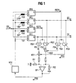
- a clock and data generator is shown in FIG . It contains four scanning flip-flops FF1 to FF4. fed. This data signal is generated by 4 clock signals TS1, TS1 , TS3 and TS3 sampled. A period of this clock signal comprises two bits of the data signal. The effective edges of the clock signals TS1 and TS1 are out of phase by 180 °. The clock signal TS3 is shifted by 90 ° with respect to the clock signal TS1. The clock signal is the same TS3 compared to the clock signal TS3 by 180 ° and the clock signal TS3 against the clock signal TS1 shifted by 90 °.
- the bits of the data signal DS are replaced by the clock signals TS1 and TS1 sampled in the middle, transferred to the scanning flip-flops FF1 and FF2 and broken down into two data signals D1 and D2, which in turn can also contain two or more data signals interleaved with one another using the time division multiplex method.
- the data signal with the clock signals TS3 and TS3 sampled, the effective edges of which coincide with the edges of the data signal.
- the sampled bits are transferred to the reference sampling flip-flops FF3 and FF4.
- phase signals PS1 and PS2 as well as PS3 and PS4 generated.
- Corresponding phase signals PS1 and PS3 as well as PS2 and PS4 are in a first adder AD1 and the phase signals PS2 and PS4 in a second adder AD2 added and then in a comparison circuit, one Operational amplifier OP, compared with each other.
- the operational amplifier is also designed as a low pass filter, so that a filtered phase locked voltage PRS from the Comparison circuit is delivered and an Osilator VCO controls which outputs the sampling clock signal TS1.
- the postponement the clock signals against each other are usually not as symbolically represented, achieved by term elements but by inverting clock signals.
Landscapes
- Engineering & Computer Science (AREA)
- Computer Networks & Wireless Communication (AREA)
- Signal Processing (AREA)
- Microelectronics & Electronic Packaging (AREA)
- Stabilization Of Oscillater, Synchronisation, Frequency Synthesizers (AREA)
- Synchronisation In Digital Transmission Systems (AREA)
Abstract
Description
Claims (4)
- Takt- und Datenregenerator mit einer ersten, zweiten und dritten Abtastkippstufe (FF1, FF2, FF3), deren Dateneingängen (D) ein Datensignal (DS) zugeführt wird, wobei der ersten Abtastkippstufe (FF1) ein erstes Taktsignal (TS1) zugeführt wird, dessen Taktperiode der Dauer von zwei Bits des Datensignals (DS) entspricht, der zweiten Abtastkippstufe (FF2) ein hierzu um 180° phasenverschobenes zweites Taktsignal (
TS1 ) zugeführt wird und der dritten Abtastkippstufe (FF3), einer Referenzabtastkippstufe, ein um 90° gegenüber einem dieser Taktsignale verschobenes drittes Taktsignal (TS3 ) zugeführt wird, mit einem ersten und einem zweiten EXOR-Element (PD1, PD2), deren erste Eingänge mit jeweils einem Ausgang der ersten und zweiten Abtastkippstufe (FF1, FF2) und deren zweite Eingänge mit einem Ausgang der dritten Abtastkippstufe (FF3) verbunden sind, mit einem Vergleichselement (OP), dessen Eingängen die Ausgangssignale der EXOR-Elemente (EXOR1, EXOR2) zugeführt werden und mit einem Oszillator (VCO), dessen Frequenz von einem gefilterten Ausgangssignal (PRS) des Vergleichelementes (OP) gesteuert wird
dadurch gekennzeichnet,dass eine vierte Abtastkippstufe (FF4) als weitere Referenz-Abtastkippstufe vorgesehen ist, der ebenfalls das Datensignal (DS) und ein um 180° gegenüber dem dritten Taktsignal phasenverschobenes viertes Taktsignal (TS3 ) zugeführt sind,dass ein drittes EXOR-Element (PD3) und ein viertes EXOR-Element (PD4) vorgesehen sind, deren erste Eingänge ebenfalls mit jeweils einem Ausgang der ersten und zweiten Abtastkippstufe (FF1, FF2) verbunden sind und deren zweite Eingänge mit einem Ausgang der vierten Abtastkippstufe (FF4) verbunden sind, und dass eine Additions- und Vergleichsschaltung ((AD1, AD2, OP) vorgesehen ist, die einander entsprechende Ausgangssignale (PS1, PS3; PS2, PS4) des ersten und des dritten EXOR-Elements (PD1, PD2) sowie des zweiten und des vierten EXOR-Elements (PD2, PD4) zusammenfaßt und vergleicht, und dass eine so gewonnenes und gefiltertes Phasenregelsignal (PRS) den Oszillators (VCO) steuert. - Takt- und Datenregenerator nach Anspruch 1,
dadurch gekennzeichnet, dass die Ausgangssignale (PS1, PS3) des ersten und dritten EXOR-Elements (PD1, PD3) sowie des zweiten und des vierten EXOR-Elements (PD2, PD4) jeweils in einem Addierer (AD1, AD2) zusammengefaßt wurden und dass die so gewonnenen Summensignale einer Vergleichsschaltung (OP) zugeführt werden. - Takt- und Datenregenerator nach Anspruch 2,
dadurch gekennzeichnet, dass als Vergleichsschaltung ein Subtrahierer (OP) vorgesehen ist ,der als Tiefpaßfilter ausgebildet ist. - Takt- und Datenregenerantor nach Anspruch 1,
dadurch gekennzeichnet, dass noch zwei weitere Abtaststufen und noch zwei weitere Referenz-Abtaststufen vorgesehen sind, die mit jeweils um 45° verschobene Taktsignale getaktet werden, wobei die Periodendauer der Taktsignale der Dauer von vier Bits des Datensignals (DS) entspricht, und dass vier Paare von EXOR-Elementen und eine Additions- und Vergleichsschaltung vorgesehen ist, die die entsprechenden Phasensignale der EXOR-Elemente addiert und die Summensignale miteinander vergleicht.
Applications Claiming Priority (2)
| Application Number | Priority Date | Filing Date | Title |
|---|---|---|---|
| DE10042233 | 2000-08-28 | ||
| DE10042233A DE10042233C2 (de) | 2000-08-28 | 2000-08-28 | Takt-und Datenregenerator mit Demultiplexerfunktion |
Publications (2)
| Publication Number | Publication Date |
|---|---|
| EP1187389A2 true EP1187389A2 (de) | 2002-03-13 |
| EP1187389A3 EP1187389A3 (de) | 2005-07-20 |
Family
ID=7654064
Family Applications (1)
| Application Number | Title | Priority Date | Filing Date |
|---|---|---|---|
| EP01119545A Withdrawn EP1187389A3 (de) | 2000-08-28 | 2001-08-14 | Takt- und Datenregenerator mit Demultiplexerfunktion |
Country Status (3)
| Country | Link |
|---|---|
| US (1) | US6888906B2 (de) |
| EP (1) | EP1187389A3 (de) |
| DE (1) | DE10042233C2 (de) |
Families Citing this family (7)
| Publication number | Priority date | Publication date | Assignee | Title |
|---|---|---|---|---|
| DE10221156B4 (de) * | 2002-05-13 | 2007-05-03 | Infineon Technologies Ag | Verfahren und Schaltungsanordnung zur Takt- und Datenrückgewinnung |
| US7627029B2 (en) | 2003-05-20 | 2009-12-01 | Rambus Inc. | Margin test methods and circuits |
| US7590175B2 (en) * | 2003-05-20 | 2009-09-15 | Rambus Inc. | DFE margin test methods and circuits that decouple sample and feedback timing |
| US7408981B2 (en) * | 2003-05-20 | 2008-08-05 | Rambus Inc. | Methods and circuits for performing margining tests in the presence of a decision feedback equalizer |
| CN101189791A (zh) * | 2005-05-24 | 2008-05-28 | 菲尼萨公司 | 噪声容限压控振荡器 |
| US8989214B2 (en) * | 2007-12-17 | 2015-03-24 | Altera Corporation | High-speed serial data signal receiver circuitry |
| TWI555338B (zh) | 2014-11-14 | 2016-10-21 | 円星科技股份有限公司 | 相位偵測器及相關的相位偵測方法 |
Family Cites Families (11)
| Publication number | Priority date | Publication date | Assignee | Title |
|---|---|---|---|---|
| US5022057A (en) * | 1988-03-11 | 1991-06-04 | Hitachi, Ltd. | Bit synchronization circuit |
| DE4231175C1 (de) * | 1992-09-17 | 1994-01-13 | Siemens Ag | Anordnung zur Taktrückgewinnung |
| US5317283A (en) * | 1993-06-08 | 1994-05-31 | Nokia Mobile Phones, Ltd. | Method to reduce noise in PLL frequency synthesis |
| JP2669347B2 (ja) * | 1994-06-15 | 1997-10-27 | 日本電気株式会社 | クロック信号抽出回路 |
| US6064707A (en) * | 1995-12-22 | 2000-05-16 | Zilog, Inc. | Apparatus and method for data synchronizing and tracking |
| DE19717586C1 (de) * | 1997-04-25 | 1998-08-27 | Siemens Ag | Takt- und Datenregenerator für hohe Datenraten |
| JP3072833B2 (ja) * | 1997-05-23 | 2000-08-07 | 日本電気株式会社 | ディジタルpll回路 |
| JP3189774B2 (ja) * | 1998-01-28 | 2001-07-16 | 日本電気株式会社 | ビット同期回路 |
| US6262611B1 (en) * | 1999-06-24 | 2001-07-17 | Nec Corporation | High-speed data receiving circuit and method |
| US6122335A (en) * | 1999-10-01 | 2000-09-19 | Quantum Bridge Communications, Inc. | Method and apparatus for fast burst mode data recovery |
| US6765975B2 (en) * | 2000-12-19 | 2004-07-20 | Intel Corporation | Method and apparatus for a tracking data receiver compensating for deterministic jitter |
-
2000
- 2000-08-28 DE DE10042233A patent/DE10042233C2/de not_active Expired - Fee Related
-
2001
- 2001-08-14 EP EP01119545A patent/EP1187389A3/de not_active Withdrawn
- 2001-08-28 US US09/941,082 patent/US6888906B2/en not_active Expired - Fee Related
Also Published As
| Publication number | Publication date |
|---|---|
| DE10042233A1 (de) | 2002-03-28 |
| DE10042233C2 (de) | 2002-07-11 |
| US6888906B2 (en) | 2005-05-03 |
| US20020064241A1 (en) | 2002-05-30 |
| EP1187389A3 (de) | 2005-07-20 |
Similar Documents
| Publication | Publication Date | Title |
|---|---|---|
| DE60308286T2 (de) | Generator zur Erzeugung eines Taktsignals mit geringem Jitter | |
| DE69922972T2 (de) | System und verfahren zum senden und empfängen von datensignalen über eine taktsignalleitung | |
| DE60029826T2 (de) | Mehrratentransportsystem sowie chipsatz | |
| DE69027574T2 (de) | Methode und Vorrichtung zur Taktrückgewinnung und Datensynchronisierung von zufälligen NRZ-Daten | |
| DE69838574T2 (de) | Phasensynchronisierungseinrichtung und Vorrichtung zum Erzeugen von in Quadraturphasenbeziehung stehenden Signalen | |
| DE69432587T2 (de) | Verzögerungsleitungsseparator für datenbus | |
| DE10157786B4 (de) | Verarbeitung von digitalen Hochgeschwindigkeitssignalen | |
| DE60122072T2 (de) | Datentaktrückgewinnungsschaltung | |
| DE69828347T2 (de) | Verfahren und Vorrichtung zum Extrahieren eines Taktsignals | |
| DE60219527T2 (de) | Takterzeugungsschaltung | |
| DE3942431C2 (de) | ||
| DE69332333T2 (de) | Synchronisierungsschaltung | |
| DE69031557T2 (de) | Zellensignalverarbeitungsschaltung und optische Vermittlungseinrichtung unter Anwendung dieser Schaltung | |
| DE69924277T2 (de) | Verfahren und schaltung für die erzeugung einer variablen taktfrequenz | |
| DE19907529B4 (de) | Vorrichtung und Verfahren zum adaptiven Ausgleichen von Arbeitszyklusstörungen | |
| DE10042233C2 (de) | Takt-und Datenregenerator mit Demultiplexerfunktion | |
| DE10130123B4 (de) | Verzögerungsregelkreis zur Erzeugung komplementärer Taktsignale | |
| WO2003096584A1 (de) | Verfahren und anordnung zur verringerung der signaldegradation eines optischen polarisation-multiplexsignals | |
| DE60107899T2 (de) | Parallele Datenschnittstelle | |
| DE102006054763A1 (de) | Differenzverstärker, Phasen- und Verzögerungsregelkreisvorrichtung und Differenzverstärkungsverfahren | |
| DE69608082T2 (de) | Mikrowellen-Mehrphasendetektor | |
| DE60201508T2 (de) | Verfahren zur Phasenkontrolle eines Datensignales, Schaltungsanordnung für gegenläufigem Takt und Interface-Vorrichtung | |
| EP0085337B1 (de) | Digitales Nachrichtenübertragungssystem | |
| DE60104974T2 (de) | Verfahren und Anordnung zur Korrektur der Taktphase in einem Datenempfänger mit einem Hogge oder Alexander Phasendiskriminator | |
| DE69531810T2 (de) | Verfahren zum Abtasten eines seriellen digitalen Signals |
Legal Events
| Date | Code | Title | Description |
|---|---|---|---|
| PUAI | Public reference made under article 153(3) epc to a published international application that has entered the european phase |
Free format text: ORIGINAL CODE: 0009012 |
|
| AK | Designated contracting states |
Kind code of ref document: A2 Designated state(s): AT BE CH CY DE DK ES FI FR GB GR IE IT LI LU MC NL PT SE TR |
|
| AX | Request for extension of the european patent |
Free format text: AL;LT;LV;MK;RO;SI |
|
| PUAL | Search report despatched |
Free format text: ORIGINAL CODE: 0009013 |
|
| AK | Designated contracting states |
Kind code of ref document: A3 Designated state(s): AT BE CH CY DE DK ES FI FR GB GR IE IT LI LU MC NL PT SE TR |
|
| AX | Request for extension of the european patent |
Extension state: AL LT LV MK RO SI |
|
| 17P | Request for examination filed |
Effective date: 20050704 |
|
| AKX | Designation fees paid |
Designated state(s): DE FR GB IT |
|
| RAP1 | Party data changed (applicant data changed or rights of an application transferred) |
Owner name: NOKIA SIEMENS NETWORKS GMBH & CO. KG |
|
| RAP3 | Party data changed (applicant data changed or rights of an application transferred) |
Owner name: NOKIA SIEMENS NETWORKS S.P.A. |
|
| RAP3 | Party data changed (applicant data changed or rights of an application transferred) |
Owner name: NOKIA SIEMENS NETWORKS GMBH & CO. KG |
|
| GRAP | Despatch of communication of intention to grant a patent |
Free format text: ORIGINAL CODE: EPIDOSNIGR1 |
|
| STAA | Information on the status of an ep patent application or granted ep patent |
Free format text: STATUS: THE APPLICATION IS DEEMED TO BE WITHDRAWN |
|
| 18D | Application deemed to be withdrawn |
Effective date: 20090303 |