EP1187221A2 - Linearer Farb-Bildsensor mit IR-Filter, und Herstellungsmethode hierfür - Google Patents
Linearer Farb-Bildsensor mit IR-Filter, und Herstellungsmethode hierfür Download PDFInfo
- Publication number
- EP1187221A2 EP1187221A2 EP01121303A EP01121303A EP1187221A2 EP 1187221 A2 EP1187221 A2 EP 1187221A2 EP 01121303 A EP01121303 A EP 01121303A EP 01121303 A EP01121303 A EP 01121303A EP 1187221 A2 EP1187221 A2 EP 1187221A2
- Authority
- EP
- European Patent Office
- Prior art keywords
- photosites
- image
- filter layer
- semiconductor chips
- color filter
- Prior art date
- Legal status (The legal status is an assumption and is not a legal conclusion. Google has not performed a legal analysis and makes no representation as to the accuracy of the status listed.)
- Granted
Links
- 238000000034 method Methods 0.000 title claims abstract description 34
- 239000004065 semiconductor Substances 0.000 claims description 56
- 239000004642 Polyimide Substances 0.000 claims description 24
- 229920001721 polyimide Polymers 0.000 claims description 24
- 238000000151 deposition Methods 0.000 claims description 20
- 238000004519 manufacturing process Methods 0.000 claims description 16
- 238000003491 array Methods 0.000 claims description 15
- NIXOWILDQLNWCW-UHFFFAOYSA-N acrylic acid group Chemical group C(C=C)(=O)O NIXOWILDQLNWCW-UHFFFAOYSA-N 0.000 claims description 12
- 239000000758 substrate Substances 0.000 claims description 11
- 238000001914 filtration Methods 0.000 abstract description 2
- 230000002708 enhancing effect Effects 0.000 abstract 1
- 235000012431 wafers Nutrition 0.000 description 36
- 108091008695 photoreceptors Proteins 0.000 description 24
- 229920002120 photoresistant polymer Polymers 0.000 description 20
- 238000003384 imaging method Methods 0.000 description 19
- 239000000463 material Substances 0.000 description 19
- 238000012546 transfer Methods 0.000 description 17
- 238000012545 processing Methods 0.000 description 16
- 239000002245 particle Substances 0.000 description 13
- 239000000843 powder Substances 0.000 description 12
- 238000011161 development Methods 0.000 description 10
- XUIMIQQOPSSXEZ-UHFFFAOYSA-N Silicon Chemical group [Si] XUIMIQQOPSSXEZ-UHFFFAOYSA-N 0.000 description 9
- 230000008569 process Effects 0.000 description 9
- 239000003086 colorant Substances 0.000 description 8
- 238000004140 cleaning Methods 0.000 description 7
- 238000012937 correction Methods 0.000 description 6
- 238000010586 diagram Methods 0.000 description 6
- 230000006870 function Effects 0.000 description 6
- 238000012986 modification Methods 0.000 description 5
- 230000004048 modification Effects 0.000 description 5
- 229910052710 silicon Inorganic materials 0.000 description 5
- 239000010703 silicon Substances 0.000 description 5
- 230000032258 transport Effects 0.000 description 5
- 238000004566 IR spectroscopy Methods 0.000 description 4
- 239000003795 chemical substances by application Substances 0.000 description 4
- 238000000576 coating method Methods 0.000 description 3
- 239000002131 composite material Substances 0.000 description 3
- 239000011521 glass Substances 0.000 description 3
- 150000002500 ions Chemical class 0.000 description 3
- 239000007788 liquid Substances 0.000 description 3
- 239000000049 pigment Substances 0.000 description 3
- 239000007921 spray Substances 0.000 description 3
- 238000010521 absorption reaction Methods 0.000 description 2
- 238000013459 approach Methods 0.000 description 2
- 239000006059 cover glass Substances 0.000 description 2
- 230000001934 delay Effects 0.000 description 2
- 239000000835 fiber Substances 0.000 description 2
- 230000003287 optical effect Effects 0.000 description 2
- 238000005070 sampling Methods 0.000 description 2
- 238000000926 separation method Methods 0.000 description 2
- 238000001228 spectrum Methods 0.000 description 2
- 238000003860 storage Methods 0.000 description 2
- 238000006424 Flood reaction Methods 0.000 description 1
- 238000003848 UV Light-Curing Methods 0.000 description 1
- 230000001133 acceleration Effects 0.000 description 1
- 230000008901 benefit Effects 0.000 description 1
- 238000003486 chemical etching Methods 0.000 description 1
- 239000011248 coating agent Substances 0.000 description 1
- 238000007906 compression Methods 0.000 description 1
- 230000006835 compression Effects 0.000 description 1
- 238000013144 data compression Methods 0.000 description 1
- 230000007423 decrease Effects 0.000 description 1
- 230000003111 delayed effect Effects 0.000 description 1
- 238000013461 design Methods 0.000 description 1
- 238000001514 detection method Methods 0.000 description 1
- 238000007599 discharging Methods 0.000 description 1
- 239000002019 doping agent Substances 0.000 description 1
- 238000005530 etching Methods 0.000 description 1
- 239000008187 granular material Substances 0.000 description 1
- 238000005286 illumination Methods 0.000 description 1
- 230000010354 integration Effects 0.000 description 1
- 238000002955 isolation Methods 0.000 description 1
- 239000011159 matrix material Substances 0.000 description 1
- 230000002093 peripheral effect Effects 0.000 description 1
- 230000035699 permeability Effects 0.000 description 1
- 238000001259 photo etching Methods 0.000 description 1
- 238000003825 pressing Methods 0.000 description 1
- 239000010453 quartz Substances 0.000 description 1
- 230000009467 reduction Effects 0.000 description 1
- 230000002829 reductive effect Effects 0.000 description 1
- 238000009877 rendering Methods 0.000 description 1
- VYPSYNLAJGMNEJ-UHFFFAOYSA-N silicon dioxide Inorganic materials O=[Si]=O VYPSYNLAJGMNEJ-UHFFFAOYSA-N 0.000 description 1
- 230000003068 static effect Effects 0.000 description 1
- 239000000126 substance Substances 0.000 description 1
- 238000012876 topography Methods 0.000 description 1
Images


Classifications
-
- H—ELECTRICITY
- H10—SEMICONDUCTOR DEVICES; ELECTRIC SOLID-STATE DEVICES NOT OTHERWISE PROVIDED FOR
- H10F—INORGANIC SEMICONDUCTOR DEVICES SENSITIVE TO INFRARED RADIATION, LIGHT, ELECTROMAGNETIC RADIATION OF SHORTER WAVELENGTH OR CORPUSCULAR RADIATION
- H10F39/00—Integrated devices, or assemblies of multiple devices, comprising at least one element covered by group H10F30/00, e.g. radiation detectors comprising photodiode arrays
- H10F39/10—Integrated devices
- H10F39/12—Image sensors
- H10F39/18—Complementary metal-oxide-semiconductor [CMOS] image sensors; Photodiode array image sensors
-
- H—ELECTRICITY
- H10—SEMICONDUCTOR DEVICES; ELECTRIC SOLID-STATE DEVICES NOT OTHERWISE PROVIDED FOR
- H10F—INORGANIC SEMICONDUCTOR DEVICES SENSITIVE TO INFRARED RADIATION, LIGHT, ELECTROMAGNETIC RADIATION OF SHORTER WAVELENGTH OR CORPUSCULAR RADIATION
- H10F39/00—Integrated devices, or assemblies of multiple devices, comprising at least one element covered by group H10F30/00, e.g. radiation detectors comprising photodiode arrays
- H10F39/011—Manufacture or treatment of image sensors covered by group H10F39/12
- H10F39/024—Manufacture or treatment of image sensors covered by group H10F39/12 of coatings or optical elements
Definitions
- the present invention generally relates to providing an infrared correction for substantially reducing or eliminating an infrared (IR) component in the information collected by image sensors as would be found in digital scanners, copiers, facsimile machines, or other document generating or reproducing device. More specifically, the present invention relates to subsampling a subset of IR coated red or blue photosites in a sensor array to provide an infrared correction for substantially reducing or eliminating an (IR) component in the information collected by image sensors.
- the present invention is particularly applicable to color input imaging devices or systems.
- Infrared optical filters have been used for a variety of instruments and applications to filter out long wavelength invisible light energy. Typical uses include UV curing units, scanning instruments and other sensing applications as shown in the sales literature, SWP & LWP Filter Coatings for Glass Substrates, which is provided by Evaporated Coatings, Inc., for example.
- Image sensor arrays typically comprise a linear array of photosensors which raster scan an image bearing document and convert the microscopic image areas viewed by each photosensor to electrical image signal charges. Following an integration period, the image signal charges are amplified and transferred as an analog video signal to a common output line or bus through successively actuated multiplexing transistors.
- One example of such an array is a charged-coupled device (CCD).
- CCD charged-coupled device
- a preferred design includes an array of photosensors of a width comparable to the width of a page being scanned, to permit one-to-one imaging generally without the use of reductive optics.
- relatively large silicon structures must be used to define the large number of photosensors.
- a preferred technique to create such a large array is to align several silicon chips end-to-end, each chip defining a small linear array thereon.
- the silicon chips which are assembled end-to-end to form a single full-width array are typically created by first creating the circuitry for a plurality of individual chips on a single silicon wafer. The silicon wafer is then cut or "diced," around the circuit areas to yield discrete chips.
- the technique for dicing the chips includes a combination of chemical etching and mechanical sawing. On each chip, the photosensors are spaced with high resolution from one end of a chip to the other; the length of each diced chip from one end of the array thereon to the other requires precision dicing.
- each individual chip with a precise dimension along the linear array of photosensors, so that, when a series of chips are assembled end-to-end to form a single page-width linear array, there is a minimum disruption of spacing from an end photosensor on one chip to a neighboring photosensor at the end of a neighboring chip.
- the spacing, or pitch, across an entire full-width linear array should be consistent regardless of the configuration of silicon chips forming the array.
- the full-width array extends the entire length of a document, such as eleven inches.
- the full-width array is used to scan line by line across the width of a document with the document being moved or stepped lengthwise in synchronism therewith.
- a typical architecture for such a sensor array is given, for example, in US Patent No. 5,473,513.
- one technique is to provide on each semiconductor chip multiple parallel linear arrays of photosensors, each of the parallel arrays being sensitive to one primary color.
- this arrangement can be achieved by providing multiple linear arrays of photosensors which are physically identical except for a selectively transparent primary-color overlay over the photosensitive areas, or "photosites,” for that linear array.
- the linear array which is supposed to be sensitive to red light only will have a transparent red layer placed on the photosites thereof, and such would be the case for a blue-sensitive array, a green-sensitive array, or any other color-sensitive array.
- These transparent layers are also referred to as absorption filter layers, because they selectively adsorb or block light having certain frequencies or wavelengths from reaching the photosensitive areas.
- absorption filter layers because they selectively adsorb or block light having certain frequencies or wavelengths from reaching the photosensitive areas.
- it is preferable to use three linear arrays any number of linear arrays can be used. As the chips are exposed to an original full-color image, only those portions of the image, which correspond to particular primary colors, will reach those photosensors assigned to the primary color.
- polyimide or acrylic The most common substances for providing these selectively transparent filter layers over the photosites are polyimide or acrylic.
- polyimide is typically applied in liquid form to a batch of photosensor chips while the chips are still in undiced, wafer form. After the polyimide liquid is applied to the wafer, the wafer is centrifuged to provide an even layer of a particular polyimide.
- a typical technique is to first apply an even layer of polyimide over the entire main surface of the chip (while the chip is still part of the wafer) and then remove the unnecessary parts of the filter by photo-etching or another well known technique.
- the entire filter layer placed over the chip is removed except for those areas over the desired set of photosites.
- Acrylic is applied to the wafer in a similar manner.
- a glass cover is placed over the chips and mounted on the substrate to provide physical protection of the chips.
- the glass cover is clear and transmits all light including infrared light.
- infrared light received by the photosites can be mistakenly interpreted as visible light by the photosites, which decreases image quality.
- a method for fabricating semiconductor chips including: providing a semiconductor wafer having a main surface defining chip areas, the chip areas defining bonding pads and three linear arrays of photosites; depositing a clear layer on the semiconductor wafer; depositing a first primary color filter layer on a first linear array of photosites; depositing a second primary color filter layer on a second linear array of photosites; depositing a third primary color filter layer on alternate photosites of a third linear array of photosites; and depositing an infrared filter layer on the photosites in the third linear array, which do not have a color filter layer.
- the method for fabricating a semiconductor chips further includes dicing the semiconductor wafer to provide semiconductor chips.
- the method of fabricating semiconductor chips further including assembling the semiconductor chips end to end on a substrate to form a full width array.
- the method of fabricating semiconductor chips, wherein the primary color filter layers consist of acrylic.
- the method of fabricating semiconductor chips, wherein the third primary color filter layer is blue.
- a method for fabricating semiconductor chips including providing a semiconductor wafer having a main surface defining chip areas, the chip areas defining bonding pads and three linear arrays of photosites; depositing a clear layer on the semiconductor wafer; depositing a first primary color filter layer on a first linear array of photosites; depositing a second primary color filter layer on alternate photosites of a second linear array of photosites; depositing a third primary color filter layer on a third linear array of photosites; and depositing an infrared filter layer on the photosites in the second linear array, which do not have a color filter layer.
- the method for fabricating a semiconductor chips further includes dicing the semiconductor wafer to provide semiconductor chips.
- the method of fabricating semiconductor chips further includes assembling the semiconductor chips end to end on a substrate to form a full width array.
- the method of fabricating semiconductor chips, wherein the infrared filter layer consists of polyimide.
- the method of fabricating semiconductor chips, wherein the primary color filter layers consist of polyimide.
- the method of fabricating semiconductor chips, wherein the primary color filter layers consist of acrylic.
- the method of fabricating semiconductor chips, wherein the second primary color filter layer is red.
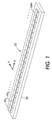
- Figure 1 shows a full width array image sensor 21 including a plurality of photosensitive chips 10 mounted end-to-end on a substrate 20 to form an effective collinear array of photosites, which extends across a page image being scanned for a scanner, copier, facsimile machine or other document reading or generating device.
- each individual photosite is adapted to output a charge or voltage signal indicative of the intensity of light of a certain type impinging thereon.
- Various structures, such as transfer circuits, or charged coupled devices, are known in the art for processing signal output by the various photosites.
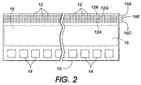
- FIG. 2 is a plan view showing one of these photosensitive chips 10 relevant to the claimed invention.
- the photosensitive chip 10 is generally made of a semiconductor substrate, as is known in the art, in which circuitry and other elements are formed, such as by photolithographic etching.
- a few of the most relevant structures are one or more linear arrays of photosites 12, each of which forms the photosensitive surface of circuitry within the photosensitive chip 10, and a set of bonding pads 14.
- the photosites 12 are typically arranged in a linear array along one main dimension of the photosensitive chip 10, with each photosite 12 along the array corresponding to one pixel in an image signal.
- the photosites 12 are preferably for sensing the three primary colors, blue, green and red.
- Photosites 12 which sense blue, green and red, are referred to as photosites 12B, 12G and 12R. However, the photosites 12 sensing blue, green and red could be replaced with photosites sensing yellow, magenta and cyan, for example. Any other suitable combination of color sensitive photosites may also be used.
- Each photosite is associated with a corresponding photosensor. Preferably, there are three parallel linear arrays 16a, 16b , and 16c for the three primary colors.
- the bonding pads 14 are distinct surfaces on the main surface of the photosensitive chip 10, and are intended to accept wire bonds attached thereto.
- the bonding pads 14 thus serve as the electronic interface between the photosensitive chip 10 and any external circuitry.
- the circuitry for obtaining signals related to light directed to the photosites 12, and for unloading image data from the photosensitive chip 10 is generally indicated as 15.
- the circuitry 15 is generally deposited between a linear array of photosites 12 and a linear array of bonding pads 14. However, any number of multiple parallel linear arrays may be provided on each photosensitive chip 10.
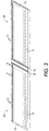
- Photosensitive chips 10 are typically formed in batches on semiconductor wafers, which are subsequently cleaved, or "diced," to create individual photosensitive chips.
- the semiconductor wafers are made of silicon.
- photolithographically etched V-grooves 18 define precisely the intended boundaries of a particular photosensitive chip 10 for dicing as shown in the perspective view of two adjacent photosensitive chips 10 in Figure 3.
- all of the photosites 12, bonding pads 14 and circuitry 15 for relatively large number of photosensitive chips 10 are etched simultaneously onto a single semiconductor wafer.
- the region between the V-grooves 18 is called the tab region.
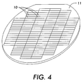
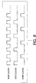
- FIG. 4 shows a typical semiconductor wafer 11, in isolation, wherein a relatively large number of photosensitive chips 10 are created in the wafer 11 prior to dicing thereof.
- Each photosensitive chip 10 has a distinct photosensitive chip area within the main surface of the wafer 11.
- the phrase "chip area" refers to a defined area within the main surface of the wafer 11 which is intended to comprise a discrete photosensitive chip 10 after the dicing step, when individual photosensitive chips 10 ( Figure 2) are separated from the rest of the wafer 11.
- the filters for the primary colors red, green and blue transmit wavelengths in both the visible region (approximately 400 nanometers to 700 nanometers) and infrared region (approximately 700 nanometers to one micron).
- the photosites 12 receive light, the light is converted into electrical signals and transmitted to a processing unit, which is typically part of a scanner.
- the processing unit recognizes the various colors of the original image by analyzing the wavelengths of the light detected by the photosites 12.
- the red, green and blue rows of photosites also sense light from the infrared region of the spectrum, thus rendering colors that are different from the original image. If the infrared component is eliminated, the photosites 12 will provide electrical signals to the processing unit, which more accurately represent the original image. Therefore, this will enhance the quality of the image output from the digital device.
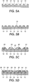
- Figures 5A-5D are cross sectional views along the line 5-5 in the direction of the arrows in Figure 3, showing polyimide or acrylic layers deposited on a row of photosites on the semiconductor wafer in accordance with the present invention.
- All three rows of photosites on the whole are preferably identical as circuit elements except that the surface of each photosite is superimposed thereon by a distinct selectively transparent color filter layer 23 or a distinct selectively transparent infrared filter layer 24.
- color filter layers 23 preferably comprise a polyimide or acrylic which has been doped with a commercially-available dye or pigment blended to yield a particular color.
- the infrared filter layer 24 of the preferred embodiment is polyimide based. It contains a dye or pigment that absorbs visible light and transmits the infrared portion of the spectrum.
- the semiconductor wafer 20 is partially planarized by using clear layer 22, which is preferably a clear polyimide or acrylic layer ( Figures 5A-5B).
- This clear layer 22 acts to smoothen the topography of the semiconductor wafer 11.
- This planarizing clear layer on the semiconductor wafer 11 is soft baked (partially baked). Certain undesirable portions of this layer are removed by means of standard photo-processing techniques.
- the bonding pads 14 shown in Figures 2-3 are examples of the areas where the clear layer is removed.
- the clear layer 22 is not removed from the photosites 12 as shown in Figure 5. After the undesirable portions of the layer have been removed, the layer is hard baked.
- the following steps are preferably performed.
- Photo-expose exposurese to ultraviolet light
- the layer removes undesirable portions of the green layer, as defined by the mask.
- the following steps are preferably performed.
- Figure 5C is a cross section of a row of photosites 12 showing the application of one color filter layer 25 (e.g. red) to the silicon wafer regardless of the chosen method.
- the odd photosites of the red row for example, are coated with a red filter layer 23 as shown in Figures 5C-5D while the even photosites are coated with the infrared (IR) transmissive filter (visible absorbing) 24 as shown in Figure 5D .
- the method used to provide the IR filter layer 24 follows the polyimide process described above. Spin coat the wafer 11 with the IR polyimide layer 24 and soft bake the layer. Spin coat the above with a layer of photoresist and bake. Photo-expose the photoresist through a mask.
- the IR filter layer 24 could be acrylic and follow the acrylic process.
- Figure 5D is a cross section of a row of photosites 12 showing the application of a red color filter layer 23 and infrared filter layer 24 to the silicon wafer regardless of the chosen method.
- the even photosites of each row could be coated with the red filter material 23 and the odd photosites of each row could be coated with the infrared filter material 24.
- alternating red coated photosites and infrared coated photosites provide pixel data, which are used to provide enhanced image quality.
- the other two rows of photosites are coated with blue or green filter layers.
- both the red and IR portions of the image are subsampled, i.e. they are read at half the base resolution.
- the base resolution of the sensor is 600 spots per inch (spi)
- both the red and IR information are collected at a resolution of 300 spi.
- a lower resolution red or blue information content does not affect the quality of the image.
- the key advantage of this approach is a double cost reduction through avoidance of an IR rejecting filter in the optical path of the scanner and through the use of a normal three row sensor (avoiding the need for a special four row sensor).
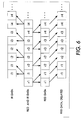
- Figures 6-8 show a sub-sampling process where, as part of a color scan, the red information (for example) is sub-sampled along with the infrared (IR) information. Both samples are taken on the same row of photosites, shown in Figures 6 and 7 as "Red and IR Data".
- the red samples in this example, correspond to the odd samples of the full base resolution.
- the IR samples are the even base resolution samples.
- each photosensitive chip 10 on the full width array image sensor 21 contains at least one linear array of photosites of the present invention, which converts the microscopic image areas viewed by each photosite into an electrical image signal charge.
- the A/D converter 25 converts the image signal to a digital image signal containing both red data and IR data.
- the red and IR data are separated by utilizing the subsampling technique described above. It must be understood that this description of alternating red and infrared photosites (subsampling) represents only one preferred embodiment for achieving this IR detection.
- Another approach could consist of placing the IR filter layer on photosites number 3,6,9, etc and the red filter layer on photosites 1 & 2, 4 & 5, 7 & 8, etc.
- any of these subsampling techniques could be applied to the blue row instead of the red row.
- the green row is preferably not subsampled as it is normally used to capture all the high resolution information of the image.
- it is preferable to have only the alternating red and infrared photosites on one row or blue and infrared photosites on one row as shown in Figure 5D alternating infrared and blue photosites in one row and alternating red and infrared rows on a second row both associated with subsampling techniques is another embodiment.
- the cost of this embodiment is higher. Therefore, the preferred embodiment is one row of photosites having alternating infrared and color filter layers.
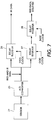
- Figure 9 is an example of a digital scanner, such as the digital scanner of U. S. Application Serial No. 09/452,690, which may include the full width array of the present invention.
- Figure 9 is a block diagram illustrating the electronic architecture of a digital scanner 30 including the scanning unit 35 employing the full width array of the present invention.
- the digital scanning unit 35 is coupled to a workstation 50 by way of a scanner interface 40.
- An example of a scanner interface 40 is a SCSI interface.
- Examples of the workstation 50 include a personal computer and a computer terminal.
- the workstation 50 includes and/or accesses a storage medium 52.
- the workstation 50 is preferably adapted to communicate with a computer network 54, and to communicate with the Internet either directly or through the computer network 54.
- the digital scanner 35 is preferably coupled to at least one image output terminal (IOT) 60, such as a printing system.
- IOT image output terminal
- the digital scanning unit 35 scans an image and converts the analog signals received by the image sensing unit 21 into digital signals (digital data).
- An image processing unit 70 registers each image, and preferably executes signal correction to enhance the digital signals.
- the FIFO (first in first out buffer) 75 temporarily stores the digital data outputted by the image processing unit 70, and transmits the digital data to the International Telecommunications Union (ITU) G3/G4 80 and Joint Photographic Experts Group (JPEG) 85 in bursts, so that the processed digital data is compressed.
- ITU International Telecommunications Union
- JPEG Joint Photographic Experts Group
- Other data compression units may be substituted for ITU G3/G4 80 and JPEG 85.
- the compressed digital data is stored in memory 100 preferably by way of Peripheral Component Interconnect Direct Memory Access (PCI DMA) Controller 90 and video bus 95.
- PCI DMA Peripheral Component Interconnect Direct Memory Access
- an operator may not wish to compress the digital data. The operator may bypass the compression step so that the digital data processed by the image processing unit 70 is sent through the FIFO 75 and directly stored in memory 100 by way of PCI DMA Controller 90.
- a computing unit 110 such as a microprocessor, is coupled to the scanner interface 40, memory 100 and PCI DMA Controller 90 by way of the video bus 95 and video bus bridge 120.
- the computing unit 110 is also coupled to a FLASH 130, static RAM 130, and display 150.
- the computing unit 110 is also connected to the scanning unit 20 and the image processing unit 70 by way of a control/data bus.
- the computing unit 110 may be communicating with the image processing unit 70 through the video bus 95 and/or PCI DMA Controller 90.
- the computing unit 110 may communicate directly with different components such as the image processing unit 70 by way of control/data bus(es) (not shown).
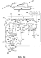
- Figure 10 is a partial schematic view of an example of a digital imaging system, such as the digital imaging system of U. S. Application Serial No. 08/838,630, including a scanner, which can utilize the full width array of the present invention. It will be understood, however, that it is not intended to limit the invention to the embodiment disclosed. On the contrary, it is intended to cover all alternatives, modifications and equivalents as may be included within the spirit and scope of the invention as defined by the appended claims.
- the RIS 228 contains document illumination lamps, optics, a mechanical scanning device and a plurality of photosensitive chips 10 of the present invention.
- the photosensitive chips 10 may include a linear array of photosites or multiple parallel linear arrays of photosites as described above.
- the RIS 228 captures the entire original document and converts it to a series of raster scan lines. This information is transmitted to an electronic subsystem (ESS) or controller 229 which controls a raster output scanner (ROS) 230.
- ESS electronic subsystem
- ROS raster output scanner
- the RIS 228 is preferably the digital scanner 30 in Figure 9 .
- the digital imaging system employs a photoconductive belt 210.
- the photoconductive belt 210 is made from a photoconductive material coated on a ground layer, which, in turn, is coated on an anti-curl backing layer.
- Belt 210 moves in the direction of arrow 213 to advance successive portions sequentially through the various processing stations deposited about the path of movement thereof.
- Belt 210 is entrained about stripping roller 214, tensioning roller 220 and drive roller 216. As roller 216 rotates, it advances belt 210 in the direction of arrow 213.
- a corona generating device indicated generally by the reference numeral 222 charges the photoconductive belt 210 to a relatively high, substantially uniform potential.
- a controller or electronic subsystem (ESS) 229 receives the image signals representing the desired output image and processes these signals to convert them to a continuous tone or grayscale rendition of the image which is transmitted to a modulated output generator, for example the raster output scanner (ROS), indicated generally by reference numeral 230.
- ESS 229 is a self-contained, dedicated minicomputer.
- the image signals transmitted to ESS 229 may originate from a RIS 228 as described above or another type of scanner utilizing the photosensitive chips 10, thereby enabling the absorption to serve as a remotely located printer for one or more scanners.
- the printer may serve as a dedicated printer for a high-speed computer or for one or more personal computers.
- ROS 230 includes a laser with rotating polygon mirror blocks.
- the ROS 230 will expose the photoconductive belt 210 to record an electrostatic latent image thereon corresponding to the continuous tone image received from ESS 229.
- ROS 230 may employ a photosensitive array of light emitting diodes (LEDs) arranged to illuminate the charged portion of photoconductive belt 210 on a raster-by-raster basis.
- LEDs light emitting diodes
- belt 210 advances the latent image to a development station, C, where toner, in the form of liquid or dry particles, is electrostatically attracted to the latent image using commonly known techniques.
- the latent image attracts toner particles from the carrier granules forming a toner powder image thereon.
- a toner particle dispenser indicated generally by the reference numeral 244, dispenses toner particles into developer housing 246 of developer unit 238.
- sheet feeding apparatus 250 includes a nudger roll 251 which feeds the uppermost sheet of stack 254 to nip 255 formed by feed roll 252 and retard roll 253.
- Feed roll 252 rotates to advance the sheet from stack 254 into vertical transport 256.
- Vertical transport 256 directs the advancing sheet 248 of support material into the registration transport 290 and past image transfer station D to receive an image from photoreceptor belt 210 in a timed sequence so that the toner powder image formed thereon contacts the advancing sheet 248 at transfer station D.
- Transfer station D includes a corona-generating device 258, which sprays ions onto the backside of sheet 248. This attracts the toner powder image from photoconductive surface 212 to sheet 248. The sheet is then detached from the photoreceptor by corona generating device 259 which sprays oppositely charged ions onto the back side of sheet 248 to assist in removing the sheet from the photoreceptor. After transfer, sheet 248 continues to move in the direction of arrow 260 by way of belt transport 262, which advances sheet 248 to fusing station F.
- Fusing station F includes a fuser assembly indicated generally by the reference numeral 270 which permanently affixes the transferred toner powder image to the copy sheet.
- fuser assembly 270 includes a heated fuser roller 272 and a pressure roller 274 with the powder image on the copy sheet contacting fuser roller 272.
- the pressure roller 274 is loaded against the fuser roller 272 to provide the necessary pressure to fix the toner powder image to the copy sheet.
- the fuser roller 272 is internally heated by a quartz lamp (not shown).
- Release agent stored in a reservoir (not shown), is pumped to a metering roll (not shown).
- a trim blade (not shown) trims off the excess release agent.
- the release agent transfers to a donor roll (not shown) and then to the fuser roll 272.
- release agent is stored in a presoaked web (not shown) and applied to the fuser roll 272 by pressing the web against fuser roll 272 and advancing the web at a slow speed.
- the sheet then passes through fuser 270 where the image is permanently fixed or fused to the sheet.
- a gate 280 either allows the sheet to move directly via output 284 to a finisher or stacker, or deflects the sheet into the duplex path 300, specifically, first into single sheet inverter 282 here. That is, if the sheet is either a simplex sheet, or a completed duplex sheet having both side one and side two images formed thereon, the sheet will be conveyed via gate 280 directly to output 284.
- the gate 280 will be positioned to deflect that sheet into the inverter 282 and into the duplex loop path 300, where that sheet will be inverted and then fed to acceleration nip 202 and belt transports 310, for recirculation back through transfer station D and fuser 270 for receiving and permanently fixing the side two image to the backside of that duplex sheet, before it exits via exit path 284.
- Cleaning station E includes a rotatably mounted fibrous brush in contact with photoconductive surface 212 to disturb and remove paper fibers and a cleaning blade to remove the nontransferred toner particles.
- the blade may be configured in either a wiper or doctor position depending on the application.
- a discharge lamp (not shown) floods photoconductive surface 212 with light to dissipate any residual electrostatic charge remaining thereon prior to the charging thereof for the next successive imaging cycle.
- Controller or ESS 229 regulates the various printer functions.
- the controller or ESS 229 is preferably a programmable microprocessor, which controls all of the printer functions hereinbefore described.
- the controller or ESS 229 provides a comparison count of the copy sheets, the number of documents being recirculated, the number of copy sheets selected by the operator, time delays, jam corrections, etc.
- the control of all of the exemplary systems heretofore described may be accomplished by conventional control switch inputs from the printing machine consoles selected by the operator.
- Conventional sheet path sensors or switches may be utilized to keep track of the position of the document and the copy sheets.
- Figure 11 is a partial schematic view of an example of a print engine of a digital imaging system, which includes a scanner having the full width array of the present invention.
- the imaging system is used to produce color output in a single pass of a photoreceptor belt. It will be understood, however, that it is not intended to limit the invention to the embodiment disclosed. On the contrary, it is intended to cover all alternatives, modifications and equivalents as may be included within the spirit and scope of the invention as defined by the appended claims, including a multiple pass color process system, a single or multiple pass highlight color system and a black and white printing system.
- the digital scanner 30 including the full width array of the present invention captures the original document (images) and converts it to digital data. This information is transmitted to an electronic subsystem (ESS) or print engine controller 700.
- digital scanner 30 captures the original document and converts it to digital data, and transmits the digital data to the workstation 50.
- the workstation 50 supplies the digital data to print engine controller 700.
- image signals may be supplied by a computer network 54 to print engine controller 700 by way of a workstation 50.
- An image-processing controller 705 receives the document information from the print engine controller 700 and converts this document information into electrical signals for the raster output scanner.
- Modern scanners connected to copiers, printers, computers, networks, facsimile machines, etc. are capable of scanning and producing complex and interesting page images.
- the pages may include text, graphics, and scanned or computer-generated images.
- the image of a page may be described as a collection of simple image components or primitives (characters, lines, bitmaps, colors, etc.).
- Complex pages can then be built by specifying a large number of the basic image primitives. This is done in software using a page description language such as PostScript.
- the job of the electronic printer's software is to receive and interpret each of the imaging primitives for the page.
- the drawing or rasterization must be done on an internal, electronic model of the page. All image components must be collected and the final page image must be assembled before marking can begin.
- the electronic model of the page is often constructed in a data structure called an image buffer.
- the data contained is in the form of an array of color values called pixels.
- Each actual page and the pixel's value give the color, which should be used when marking.
- the pixels are organized to reflect the geometric relation of their corresponding spots. They are usually ordered to provide easy access in the raster pattern required for marking.
- the printing machine preferably uses a charge retentive surface in the form of an Active Matrix (AMAT) photoreceptor belt 710 supported for movement in the direction indicated by arrow 712, for advancing sequentially through the various xerographic process stations.
- AMAT Active Matrix
- the photoreceptor belt 710 is entrained about a drive roller 714, tension rollers 716 and fixed roller 718 and the drive roller 714 is operatively connected to a drive motor 720 for effecting movement of the photoreceptor belt 710 through the xerographic stations.
- a portion of photoreceptor belt 710 passes through charging station A where a corona generating device, indicated generally by the reference numeral 722, charges the photoconductive surface of photoreceptor belt 710 to a relatively high, substantially uniform, preferably negative potential.
- the print engine controller 700 receives the image signals representing the desired output image from the digital scanner 30 directly, computer network 54, or work station 50 and processes these signals to convert them to the various color separations of the image.
- the desired output image is transmitted to a laser based output scanning device, which causes the charge retentive surface to be discharged in accordance with the output from the scanning device.
- the laser based scanning device is a laser Raster Output Scanner (ROS) 724.
- ROS 724 could be replaced by other xerographic exposure devices such as an LED array.
- the photoreceptor belt 710 which is initially charged to a voltage V 0 , undergoes dark decay to a level equal to about -500 volts. When exposed at the exposure station B, it is discharged to a level equal to about -50 volts. Thus after exposure, the photoreceptor belt 710 contains a monopolar voltage profile of high and low voltages, the former corresponding to charged areas and the latter corresponding to discharged or background areas.
- the development station C preferably utilizes a hybrid development system including a developer structure 730.
- the development roll better known as the donor roll, is powered by two development fields (potentials across an air gap).
- the first field is the ac field which is used for toner cloud generation.
- the second field is the dc development field which is used to control the amount of developed toner mass on the photoreceptor belt 710.
- the developer structure 730 contains magenta toner particles 732.
- the toner cloud causes charged magenta toner particles 732 to be attracted to the electrostatic latent image.
- Appropriate developer biasing is accomplished via a power supply (not shown).
- This type of system is a noncontact type in which only toner particles (magenta, for example) are attracted to the latent image and there is no mechanical contact between the photoreceptor belt 710 and a toner delivery device to disturb a previously developed, but unfixed, image.
- a toner concentration sensor 800 senses the toner concentration in the developer structure 730.
- a dispenser 734 dispenses magenta toner into the developer structure 730 to maintain a proper toner concentration. The dispenser 734 is controlled by print engine controller 700.
- the developed but unfixed image is then transported past a second charging device 810 where the photoreceptor belt 710 and previously developed toner image areas are recharged to a predetermined level.
- a second exposure/imaging is performed by device 820 which preferably comprises a laser based output structure.
- the device 820 is utilized for selectively discharging the photoreceptor belt 710 on toned areas and/or bare areas, pursuant to the image to be developed with the second color toner.
- Device 820 may be a raster output scanner or LED bar, which is controlled by print engine controller 700.
- the photoreceptor belt 710 contains toned and untoned areas at relatively high voltage levels and toned and untoned areas at relatively low voltage levels. These low voltage areas represent image areas which are developed using discharged area development (DAD).
- DAD discharged area development
- a negatively charged, developer material 742 comprising the second color toner, preferably yellow, is employed.
- the second color toner is contained in a developer structure 740 disposed at a second developer station D and is presented to the latent images on the photoreceptor belt 710 by way of a second developer system.
- a power supply (not shown) serves to electrically bias the developer structure 740 to a level effective to develop the discharged image areas with negatively charged yellow toner particles 742.
- a toner concentration sensor 800 senses the toner concentration in the developer structure 740.
- a dispenser 744 dispenses magenta toner into the developer structure 740 to maintain a proper toner concentration. The dispenser 744 is controlled by print engine controller 700.
- developer structures 730, 740, 750 and 760 are the same or similar in structure.
- dispensers 734, 744, 754 and 764 are the same or similar in structure.
- the exposure control scheme described below may be utilized for these subsequent imaging steps. In this manner a full color composite toner image is developed on the photoreceptor belt 710.
- a permeability sensor 830 measures developed mass per unit area (developability). Although only one sensor 830 is shown in Figure 11, there may be more than one sensor 830.
- a negative pre-transfer dicorotron member 770 is provided to condition all of the toner for effective transfer to a substrate.
- a sheet of support material 840 is moved into contact with the toner images at transfer station G.
- the sheet of support material 840 is advanced to transfer station G by the supply unit 845 in the direction of arrow 850.
- the sheet of support material 840 is then brought into contact with photoconductive surface of photoreceptor belt 710 in a timed sequence so that the toner powder image developed thereon contacts the advancing sheet of support material 840 at transfer station G.
- Transfer station G includes a transfer dicorotron 772 which sprays positive ions onto the backside of support material 840. This attracts the negatively charged toner powder images from the photoreceptor belt 710 to support material 840.
- a detack dicorotron 774 is provided for facilitating stripping of the sheets from the photoreceptor belt 710 .
- Fusing station H includes a fuser assembly, indicated generally by the reference numeral 780, which permanently affixes the transferred powder image to support material 840.
- fuser assembly 780 comprises a heated fuser roller 782 and a backup or pressure roller 784.
- Support material 840 passes between fuser roller 782 and backup roller 784 with the toner powder image contacting fuser roller 782. In this manner, the toner powder images are permanently affixed to support material 840.
- a chute guides the advancing sheets 28 to a catch tray, stacker, finisher or other output device (not shown), for subsequent removal from the printing machine by the operator.
- the residual toner particles carried by the non-image areas on the photoconductive surface are removed therefrom. These particles are removed at cleaning station I using a cleaning brush or plural brush structure contained in a housing 790.
- the cleaning brush 795 or brushes 795 are engaged after the composite toner image is transferred to a sheet. Once the photoreceptor belt 710 is cleaned the brushes 795 are retracted utilizing a device incorporating a clutch (not shown) so that the next imaging and development cycle can begin.
- Print engine controller 700 regulates the various printer functions.
- the print engine controller 700 preferably includes one or more programmable controllers, which control printer functions hereinbefore described.
- the print engine controller 700 may also provide a comparison count of the copy sheets, the number of documents being recirculated, the number of copy sheets selected by the operator, time delays, jam corrections, etc.
- the control of all of the exemplary systems heretofore described may be accomplished automatically, through the use of user interface 860 from the printing machine consoles selected by an operator, or through the use of a workstation 50 selected by the operator.
- Conventional sheet path sensors or switches may be utilized to keep track of the position of the document and the copy sheets.
- Figures 9-11 show examples of a digital imaging systems incorporating the digital scanner 30 including the full width array of the present invention, it is understood that this full width array could be used in any imaging system having any number of developer structures.
Landscapes
- Facsimile Heads (AREA)
- Solid State Image Pick-Up Elements (AREA)
- Image Input (AREA)
Applications Claiming Priority (2)
| Application Number | Priority Date | Filing Date | Title |
|---|---|---|---|
| US09/656,879 US6316284B1 (en) | 2000-09-07 | 2000-09-07 | Infrared correction in color scanners |
| US656879 | 2000-09-07 |
Publications (3)
| Publication Number | Publication Date |
|---|---|
| EP1187221A2 true EP1187221A2 (de) | 2002-03-13 |
| EP1187221A3 EP1187221A3 (de) | 2005-01-19 |
| EP1187221B1 EP1187221B1 (de) | 2008-06-04 |
Family
ID=24634951
Family Applications (1)
| Application Number | Title | Priority Date | Filing Date |
|---|---|---|---|
| EP01121303A Expired - Lifetime EP1187221B1 (de) | 2000-09-07 | 2001-09-05 | Linearer Farb-Bildsensor mit IR-Filter, und Herstellungsmethode hierfür |
Country Status (4)
| Country | Link |
|---|---|
| US (1) | US6316284B1 (de) |
| EP (1) | EP1187221B1 (de) |
| JP (1) | JP2002176530A (de) |
| DE (1) | DE60134297D1 (de) |
Cited By (1)
| Publication number | Priority date | Publication date | Assignee | Title |
|---|---|---|---|---|
| DE10247819A1 (de) * | 2002-10-14 | 2004-04-22 | Infineon Technologies Ag | Verfahren zum Herstellen einer Sensor-Anordnung, Sensor-Anordnung und Digitalkamera |
Families Citing this family (5)
| Publication number | Priority date | Publication date | Assignee | Title |
|---|---|---|---|---|
| US6396297B1 (en) * | 2000-12-14 | 2002-05-28 | Xerox Corporation | Electrical detection of V-groove width |
| US6834855B2 (en) * | 2001-10-09 | 2004-12-28 | Edward J. Mancuso | Dice scanner |
| US20090159799A1 (en) * | 2007-12-19 | 2009-06-25 | Spectral Instruments, Inc. | Color infrared light sensor, camera, and method for capturing images |
| US20160255323A1 (en) | 2015-02-26 | 2016-09-01 | Dual Aperture International Co. Ltd. | Multi-Aperture Depth Map Using Blur Kernels and Down-Sampling |
| US10943895B2 (en) * | 2019-01-14 | 2021-03-09 | Xerox Corporation | Method of fabricating a plurality of linear arrays with submicron y-axis alignment |
Family Cites Families (75)
| Publication number | Priority date | Publication date | Assignee | Title |
|---|---|---|---|---|
| US3596635A (en) | 1967-03-16 | 1971-08-03 | Bell & Howell Co | Electrostatographic office copier |
| US4672457A (en) | 1970-12-28 | 1987-06-09 | Hyatt Gilbert P | Scanner system |
| US4739396C1 (en) | 1970-12-28 | 2002-07-09 | Gilbert P Hyatt | Projection display system |
| US3864722A (en) | 1973-05-02 | 1975-02-04 | Rca Corp | Radiation sensing arrays |
| JPS50151487A (de) | 1974-05-24 | 1975-12-05 | ||
| US4016597A (en) | 1975-09-11 | 1977-04-05 | Eastman Kodak Company | Color video camera with selectively expanded sensitivity |
| JPS5941351B2 (ja) | 1976-09-13 | 1984-10-06 | 株式会社日立製作所 | カラ−用固体撮像素子 |
| US4173765A (en) | 1978-05-26 | 1979-11-06 | Eastman Kodak Company | V-MOS imaging array |
| JPS6046401B2 (ja) | 1979-02-26 | 1985-10-16 | 株式会社日立製作所 | 固体撮像素子の製造方法 |
| US4418284A (en) | 1980-03-17 | 1983-11-29 | Matsushita Electric Industrial Co., Ltd. | Solid-state color-image sensor and process for fabricating the same |
| JPS60148269A (ja) | 1984-01-12 | 1985-08-05 | Sharp Corp | カラ−画像読取装置 |
| US4691243A (en) | 1984-05-04 | 1987-09-01 | Energy Conversion Devices, Inc. | Contact-type document scanner including protective coating |
| US4727407A (en) | 1984-07-13 | 1988-02-23 | Fuji Xerox Co., Ltd. | Image sensor |
| US5166784A (en) | 1985-10-25 | 1992-11-24 | Canon Kabushiki Kaisha | Original reading apparatus, having a filter, for reading a color original |
| EP0223880A1 (de) | 1985-10-30 | 1987-06-03 | Agfa-Gevaert N.V. | Optoelektronische Schaltung zur Erzeugung eines Bildkontrastsignals |
| US4933983A (en) | 1986-02-14 | 1990-06-12 | Canon Kabushiki Kaisha | Image data reading apparatus |
| JPS62243478A (ja) | 1986-04-16 | 1987-10-23 | Canon Inc | カラ−複写装置 |
| US4827118A (en) | 1986-07-10 | 1989-05-02 | Minolta Camera Kabushiki Kaisha | Light-sensitive device having color filter and manufacturing method thereof |
| US4737854A (en) | 1986-07-18 | 1988-04-12 | Xerox Corporation | Image sensor array with two stage transfer |
| JPS6416067A (en) | 1987-07-08 | 1989-01-19 | Minolta Camera Kk | Original detector |
| US4814296A (en) | 1987-08-28 | 1989-03-21 | Xerox Corporation | Method of fabricating image sensor dies for use in assembling arrays |
| US5024923A (en) | 1987-09-09 | 1991-06-18 | Fuji Photo Film Co., Ltd. | Infrared absorbent compositions |
| JP2692824B2 (ja) | 1987-12-29 | 1997-12-17 | 株式会社リコー | 原稿読取装置 |
| US4905039A (en) | 1988-01-14 | 1990-02-27 | Fuji Photo Film Co., Ltd. | Color image exposure apparatus |
| DE8808815U1 (de) | 1988-06-23 | 1988-09-15 | Heimann Optoelectronics Gmbh, 65199 Wiesbaden | Infrarotdetektor |
| US4862253A (en) | 1988-07-20 | 1989-08-29 | Welch Allyn, Inc. | Apparatus for converting a video processor |
| US4899214A (en) | 1988-09-02 | 1990-02-06 | Itek Graphic Corp. | Low cost color scanner |
| JPH02146772A (ja) | 1989-10-15 | 1990-06-05 | Minolta Camera Co Ltd | イメージセンサー |
| US5144498A (en) | 1990-02-14 | 1992-09-01 | Hewlett-Packard Company | Variable wavelength light filter and sensor system |
| US5105277A (en) | 1990-12-24 | 1992-04-14 | Xerox Corporation | Process for canceling cell-to-cell performance variations in a sensor array |
| US5081536A (en) | 1990-12-24 | 1992-01-14 | Xerox Corporation | Image sensor array using two stage transfer having improved uniformity |
| US5114478A (en) | 1991-01-07 | 1992-05-19 | Pitney Bowes Inc. | Homogenous ink composition |
| JP2563236Y2 (ja) | 1991-02-15 | 1998-02-18 | オリンパス光学工業株式会社 | 固体撮像装置 |
| US5159199A (en) | 1991-08-12 | 1992-10-27 | The United States Of America As Represented By The Administrator Of The National Aeronautics And Space Administration | Integrated filter and detector array for spectral imaging |
| US5153421A (en) | 1991-11-04 | 1992-10-06 | Xerox Corporation | Architecture for analog and digital image sensor arrays |
| DE4136461C2 (de) | 1991-11-06 | 1999-04-08 | Roland Man Druckmasch | Vorrichtung und Verfahren zur großflächigen Bildinspektion |
| FI88768C (fi) | 1991-11-27 | 1993-06-28 | Valtion Teknillinen | Foerfarande och anordning foer bildning av felfaergbild |
| JPH05343655A (ja) | 1992-04-01 | 1993-12-24 | Nec Corp | 固体撮像装置 |
| CA2108813C (en) | 1992-10-23 | 2002-08-06 | Shinobu Arimoto | Photo-sensor and image processing apparatus |
| US5272113A (en) * | 1992-11-12 | 1993-12-21 | Xerox Corporation | Method for minimizing stress between semiconductor chips having a coefficient of thermal expansion different from that of a mounting substrate |
| US5724152A (en) | 1993-01-01 | 1998-03-03 | Canon Kabushiki Kaisha | Image reading apparatus and image processing apparatus for reading optical information of visible and non-visible light |
| US5453611A (en) * | 1993-01-01 | 1995-09-26 | Canon Kabushiki Kaisha | Solid-state image pickup device with a plurality of photoelectric conversion elements on a common semiconductor chip |
| DE69333213T2 (de) | 1993-01-01 | 2004-06-24 | Canon K.K. | Bildlesevorrichtung |
| JPH06311302A (ja) | 1993-04-19 | 1994-11-04 | Fuji Xerox Co Ltd | カラー固体ラインセンサ |
| DE69321822T2 (de) * | 1993-05-19 | 1999-04-01 | Hewlett-Packard Gmbh, 71034 Boeblingen | Photodiodenstruktur |
| EP0629926B1 (de) | 1993-06-15 | 1998-12-09 | Sharp Kabushiki Kaisha | Bildverarbeitungsgerät |
| JP3161875B2 (ja) | 1993-06-15 | 2001-04-25 | キヤノン株式会社 | 原稿読取り装置 |
| US5340619A (en) | 1993-10-18 | 1994-08-23 | Brewer Science, Inc. | Method of manufacturing a color filter array |
| JPH07122720A (ja) | 1993-10-22 | 1995-05-12 | Canon Inc | イメージセンサー及びその製造方法 |
| US5648653A (en) | 1993-10-22 | 1997-07-15 | Canon Kabushiki Kaisha | Optical filter having alternately laminated thin layers provided on a light receiving surface of an image sensor |
| ATE183137T1 (de) | 1993-12-15 | 1999-08-15 | Goss Graphic Syst Inc | Druckereisteuerungssystem |
| US5545913A (en) | 1994-10-17 | 1996-08-13 | Xerox Corporation | Assembly for mounting semiconductor chips in a full-width-array image scanner |
| US5521125A (en) | 1994-10-28 | 1996-05-28 | Xerox Corporation | Precision dicing of silicon chips from a wafer |
| US5493423A (en) | 1994-10-28 | 1996-02-20 | Xerox Corporation | Resettable pixel amplifier for an image sensor array |
| US5489457A (en) | 1994-12-06 | 1996-02-06 | Xerox Corporation | Reflective tape |
| US5530278A (en) | 1995-04-24 | 1996-06-25 | Xerox Corporation | Semiconductor chip having a dam to prevent contamination of photosensitive structures thereon |
| US5604362A (en) | 1995-04-24 | 1997-02-18 | Xerox Corporation | Filter architecture for a photosensitive chip |
| JP3881056B2 (ja) | 1995-05-19 | 2007-02-14 | ゼロックス コーポレイション | ビデオイメージデータ出力装置 |
| US5777329A (en) | 1995-07-21 | 1998-07-07 | Texas Instruments Incorporated | Bolometer array spectrometer |
| US5841137A (en) | 1995-08-11 | 1998-11-24 | Texas Instruments Incorporated | Duplicative detector sensor |
| US5790211A (en) | 1995-09-08 | 1998-08-04 | Xerox Corporation | Platen cover for a digital document scanner with electrically switchable reflectance modes |
| US5691760A (en) | 1995-10-12 | 1997-11-25 | Xerox Corporation | Photosensitive silicon chip having photosites spaced at varying pitches |
| US5696626A (en) * | 1995-10-12 | 1997-12-09 | Xerox Corporation | Photosensitive silicon chip having a ridge near an end photosite |
| US5665963A (en) | 1996-01-24 | 1997-09-09 | Hewlett-Packard Company | Reflective color filter for color correction of photodetector filters |
| US5714759A (en) | 1996-02-23 | 1998-02-03 | Ohmeda Inc. | Optical system with an extended, imaged source |
| US5668596A (en) | 1996-02-29 | 1997-09-16 | Eastman Kodak Company | Digital imaging device optimized for color performance |
| US5834761A (en) | 1996-03-22 | 1998-11-10 | Sharp Kabushiki Kaisah | Image input apparatus having a spatial filter controller |
| US5929432A (en) * | 1996-05-30 | 1999-07-27 | Kabushiki Kaisha Toshiba | Solid state image sensing device and image sensor using the same |
| JPH1065135A (ja) | 1996-05-30 | 1998-03-06 | Toshiba Corp | 固体撮像装置およびこれを用いた画像読取装置 |
| PE73298A1 (es) | 1996-06-04 | 1998-11-13 | Coin Bill Validator Inc | Validador de billetes de banco |
| US5808297A (en) | 1996-07-22 | 1998-09-15 | Xerox Corporation | Reflective test patches for translucent color filters in photosensitive semiconductor chips |
| US6380539B1 (en) | 1997-01-30 | 2002-04-30 | Applied Science Fiction, Inc. | Four color trilinear CCD scanning |
| US5848331A (en) | 1997-04-11 | 1998-12-08 | Xerox Corporation | Fuser roll housing |
| US6211521B1 (en) | 1998-03-13 | 2001-04-03 | Intel Corporation | Infrared pixel sensor and infrared signal correction |
| US6157019A (en) * | 1999-03-31 | 2000-12-05 | Xerox Corporation | Edge photosite definition by opaque filter layer |
-
2000
- 2000-09-07 US US09/656,879 patent/US6316284B1/en not_active Expired - Lifetime
-
2001
- 2001-08-15 JP JP2001246346A patent/JP2002176530A/ja not_active Withdrawn
- 2001-09-05 EP EP01121303A patent/EP1187221B1/de not_active Expired - Lifetime
- 2001-09-05 DE DE60134297T patent/DE60134297D1/de not_active Expired - Lifetime
Cited By (2)
| Publication number | Priority date | Publication date | Assignee | Title |
|---|---|---|---|---|
| DE10247819A1 (de) * | 2002-10-14 | 2004-04-22 | Infineon Technologies Ag | Verfahren zum Herstellen einer Sensor-Anordnung, Sensor-Anordnung und Digitalkamera |
| DE10247819B4 (de) * | 2002-10-14 | 2014-10-30 | Infineon Technologies Ag | Verfahren zum Herstellen einer Bild-Sensor-Anordnung |
Also Published As
| Publication number | Publication date |
|---|---|
| JP2002176530A (ja) | 2002-06-21 |
| US6316284B1 (en) | 2001-11-13 |
| EP1187221B1 (de) | 2008-06-04 |
| EP1187221A3 (de) | 2005-01-19 |
| DE60134297D1 (de) | 2008-07-17 |
Similar Documents
| Publication | Publication Date | Title |
|---|---|---|
| US6125248A (en) | Electrostatographic reproduction machine including a plurality of selectable fusing assemblies | |
| US6252220B1 (en) | Sensor cover glass with infrared filter | |
| JP3310425B2 (ja) | 多重波長、単一光学系のrosおよび多層の感光体を有するカラー・ゼログラフィック・プリント・システム | |
| US5221954A (en) | Single pass full color printing system using a quad-level xerographic unit | |
| US6201293B1 (en) | Electro optical devices with reduced filter thinning on the edge pixel photosites and method of producing same | |
| US6654056B1 (en) | Geometric configurations for photosites for reducing Moiré patterns | |
| US5926670A (en) | Image forming apparatus cleaning an intermediate transfer member carrying a concurrently existing plurality of toner image pages | |
| US6316284B1 (en) | Infrared correction in color scanners | |
| US6768565B1 (en) | Infrared correction in color scanners | |
| US5119139A (en) | Electrophotographic image forming apparatus having multiple printing stations | |
| US6157019A (en) | Edge photosite definition by opaque filter layer | |
| US6559956B2 (en) | Butted sensor array with supplemental chip in abutment region | |
| US6249656B1 (en) | Image forming apparatus that reduces test toner cleaning | |
| US6642964B1 (en) | Geometric configurations for photosites for reducing moire patterns | |
| US6670598B1 (en) | Low power autozero of pixel amplifier | |
| US6198093B1 (en) | Electro optical devices with reduced filter thinning on the edge pixel photosites and method of producing same | |
| US6556805B1 (en) | Dual cam set transfer assist blade system | |
| US6198903B1 (en) | Reproduction machine having a stalling preventing transfer station sheet placement assembly | |
| US6026276A (en) | Apparatus for handling color transparencies using vacuum switching | |
| JPH0250174A (ja) | 電子写真記録装置 | |
| JP2000019895A (ja) | 画像処理方法及び装置並びに記憶媒体 | |
| US7471922B2 (en) | Segmented transfer assist blade | |
| JP2001042743A (ja) | 画像形成装置、画像形成方法、及び記憶媒体 | |
| US20250328104A1 (en) | Image forming apparatus | |
| JPS60238823A (ja) | 画像形成装置 |
Legal Events
| Date | Code | Title | Description |
|---|---|---|---|
| PUAI | Public reference made under article 153(3) epc to a published international application that has entered the european phase |
Free format text: ORIGINAL CODE: 0009012 |
|
| AK | Designated contracting states |
Kind code of ref document: A2 Designated state(s): AT BE CH CY DE DK ES FI FR GB GR IE IT LI LU MC NL PT SE TR |
|
| AX | Request for extension of the european patent |
Free format text: AL;LT;LV;MK;RO;SI |
|
| PUAL | Search report despatched |
Free format text: ORIGINAL CODE: 0009013 |
|
| AK | Designated contracting states |
Kind code of ref document: A3 Designated state(s): AT BE CH CY DE DK ES FI FR GB GR IE IT LI LU MC NL PT SE TR |
|
| AX | Request for extension of the european patent |
Extension state: AL LT LV MK RO SI |
|
| 17P | Request for examination filed |
Effective date: 20050719 |
|
| AKX | Designation fees paid |
Designated state(s): DE FR GB |
|
| 17Q | First examination report despatched |
Effective date: 20050823 |
|
| GRAP | Despatch of communication of intention to grant a patent |
Free format text: ORIGINAL CODE: EPIDOSNIGR1 |
|
| GRAS | Grant fee paid |
Free format text: ORIGINAL CODE: EPIDOSNIGR3 |
|
| GRAA | (expected) grant |
Free format text: ORIGINAL CODE: 0009210 |
|
| AK | Designated contracting states |
Kind code of ref document: B1 Designated state(s): DE FR GB |
|
| REG | Reference to a national code |
Ref country code: GB Ref legal event code: FG4D |
|
| REF | Corresponds to: |
Ref document number: 60134297 Country of ref document: DE Date of ref document: 20080717 Kind code of ref document: P |
|
| PLBE | No opposition filed within time limit |
Free format text: ORIGINAL CODE: 0009261 |
|
| STAA | Information on the status of an ep patent application or granted ep patent |
Free format text: STATUS: NO OPPOSITION FILED WITHIN TIME LIMIT |
|
| 26N | No opposition filed |
Effective date: 20090305 |
|
| REG | Reference to a national code |
Ref country code: FR Ref legal event code: PLFP Year of fee payment: 15 |
|
| PGFP | Annual fee paid to national office [announced via postgrant information from national office to epo] |
Ref country code: GB Payment date: 20150825 Year of fee payment: 15 Ref country code: DE Payment date: 20150820 Year of fee payment: 15 |
|
| PGFP | Annual fee paid to national office [announced via postgrant information from national office to epo] |
Ref country code: FR Payment date: 20150824 Year of fee payment: 15 |
|
| REG | Reference to a national code |
Ref country code: DE Ref legal event code: R119 Ref document number: 60134297 Country of ref document: DE |
|
| GBPC | Gb: european patent ceased through non-payment of renewal fee |
Effective date: 20160905 |
|
| REG | Reference to a national code |
Ref country code: FR Ref legal event code: ST Effective date: 20170531 |
|
| PG25 | Lapsed in a contracting state [announced via postgrant information from national office to epo] |
Ref country code: FR Free format text: LAPSE BECAUSE OF NON-PAYMENT OF DUE FEES Effective date: 20160930 Ref country code: DE Free format text: LAPSE BECAUSE OF NON-PAYMENT OF DUE FEES Effective date: 20170401 Ref country code: GB Free format text: LAPSE BECAUSE OF NON-PAYMENT OF DUE FEES Effective date: 20160905 |