EP1184713B1 - Liquid crystal display device - Google Patents
Liquid crystal display device Download PDFInfo
- Publication number
- EP1184713B1 EP1184713B1 EP01307161A EP01307161A EP1184713B1 EP 1184713 B1 EP1184713 B1 EP 1184713B1 EP 01307161 A EP01307161 A EP 01307161A EP 01307161 A EP01307161 A EP 01307161A EP 1184713 B1 EP1184713 B1 EP 1184713B1
- Authority
- EP
- European Patent Office
- Prior art keywords
- plate
- liquid crystal
- crystal display
- phase retarder
- polarizing plate
- Prior art date
- Legal status (The legal status is an assumption and is not a legal conclusion. Google has not performed a legal analysis and makes no representation as to the accuracy of the status listed.)
- Expired - Lifetime
Links
Images
Classifications
-
- G—PHYSICS
- G02—OPTICS
- G02F—OPTICAL DEVICES OR ARRANGEMENTS FOR THE CONTROL OF LIGHT BY MODIFICATION OF THE OPTICAL PROPERTIES OF THE MEDIA OF THE ELEMENTS INVOLVED THEREIN; NON-LINEAR OPTICS; FREQUENCY-CHANGING OF LIGHT; OPTICAL LOGIC ELEMENTS; OPTICAL ANALOGUE/DIGITAL CONVERTERS
- G02F1/00—Devices or arrangements for the control of the intensity, colour, phase, polarisation or direction of light arriving from an independent light source, e.g. switching, gating or modulating; Non-linear optics
- G02F1/01—Devices or arrangements for the control of the intensity, colour, phase, polarisation or direction of light arriving from an independent light source, e.g. switching, gating or modulating; Non-linear optics for the control of the intensity, phase, polarisation or colour
- G02F1/13—Devices or arrangements for the control of the intensity, colour, phase, polarisation or direction of light arriving from an independent light source, e.g. switching, gating or modulating; Non-linear optics for the control of the intensity, phase, polarisation or colour based on liquid crystals, e.g. single liquid crystal display cells
- G02F1/133—Constructional arrangements; Operation of liquid crystal cells; Circuit arrangements
- G02F1/1333—Constructional arrangements; Manufacturing methods
- G02F1/13338—Input devices, e.g. touch panels
-
- G—PHYSICS
- G02—OPTICS
- G02F—OPTICAL DEVICES OR ARRANGEMENTS FOR THE CONTROL OF LIGHT BY MODIFICATION OF THE OPTICAL PROPERTIES OF THE MEDIA OF THE ELEMENTS INVOLVED THEREIN; NON-LINEAR OPTICS; FREQUENCY-CHANGING OF LIGHT; OPTICAL LOGIC ELEMENTS; OPTICAL ANALOGUE/DIGITAL CONVERTERS
- G02F1/00—Devices or arrangements for the control of the intensity, colour, phase, polarisation or direction of light arriving from an independent light source, e.g. switching, gating or modulating; Non-linear optics
- G02F1/01—Devices or arrangements for the control of the intensity, colour, phase, polarisation or direction of light arriving from an independent light source, e.g. switching, gating or modulating; Non-linear optics for the control of the intensity, phase, polarisation or colour
- G02F1/13—Devices or arrangements for the control of the intensity, colour, phase, polarisation or direction of light arriving from an independent light source, e.g. switching, gating or modulating; Non-linear optics for the control of the intensity, phase, polarisation or colour based on liquid crystals, e.g. single liquid crystal display cells
- G02F1/133—Constructional arrangements; Operation of liquid crystal cells; Circuit arrangements
- G02F1/1333—Constructional arrangements; Manufacturing methods
- G02F1/1335—Structural association of cells with optical devices, e.g. polarisers or reflectors
- G02F1/133502—Antiglare, refractive index matching layers
-
- G—PHYSICS
- G02—OPTICS
- G02F—OPTICAL DEVICES OR ARRANGEMENTS FOR THE CONTROL OF LIGHT BY MODIFICATION OF THE OPTICAL PROPERTIES OF THE MEDIA OF THE ELEMENTS INVOLVED THEREIN; NON-LINEAR OPTICS; FREQUENCY-CHANGING OF LIGHT; OPTICAL LOGIC ELEMENTS; OPTICAL ANALOGUE/DIGITAL CONVERTERS
- G02F1/00—Devices or arrangements for the control of the intensity, colour, phase, polarisation or direction of light arriving from an independent light source, e.g. switching, gating or modulating; Non-linear optics
- G02F1/01—Devices or arrangements for the control of the intensity, colour, phase, polarisation or direction of light arriving from an independent light source, e.g. switching, gating or modulating; Non-linear optics for the control of the intensity, phase, polarisation or colour
- G02F1/13—Devices or arrangements for the control of the intensity, colour, phase, polarisation or direction of light arriving from an independent light source, e.g. switching, gating or modulating; Non-linear optics for the control of the intensity, phase, polarisation or colour based on liquid crystals, e.g. single liquid crystal display cells
- G02F1/133—Constructional arrangements; Operation of liquid crystal cells; Circuit arrangements
- G02F1/1333—Constructional arrangements; Manufacturing methods
- G02F1/1335—Structural association of cells with optical devices, e.g. polarisers or reflectors
- G02F1/13363—Birefringent elements, e.g. for optical compensation
- G02F1/133637—Birefringent elements, e.g. for optical compensation characterised by the wavelength dispersion
-
- G—PHYSICS
- G02—OPTICS
- G02F—OPTICAL DEVICES OR ARRANGEMENTS FOR THE CONTROL OF LIGHT BY MODIFICATION OF THE OPTICAL PROPERTIES OF THE MEDIA OF THE ELEMENTS INVOLVED THEREIN; NON-LINEAR OPTICS; FREQUENCY-CHANGING OF LIGHT; OPTICAL LOGIC ELEMENTS; OPTICAL ANALOGUE/DIGITAL CONVERTERS
- G02F1/00—Devices or arrangements for the control of the intensity, colour, phase, polarisation or direction of light arriving from an independent light source, e.g. switching, gating or modulating; Non-linear optics
- G02F1/01—Devices or arrangements for the control of the intensity, colour, phase, polarisation or direction of light arriving from an independent light source, e.g. switching, gating or modulating; Non-linear optics for the control of the intensity, phase, polarisation or colour
- G02F1/13—Devices or arrangements for the control of the intensity, colour, phase, polarisation or direction of light arriving from an independent light source, e.g. switching, gating or modulating; Non-linear optics for the control of the intensity, phase, polarisation or colour based on liquid crystals, e.g. single liquid crystal display cells
- G02F1/133—Constructional arrangements; Operation of liquid crystal cells; Circuit arrangements
- G02F1/1333—Constructional arrangements; Manufacturing methods
- G02F1/1335—Structural association of cells with optical devices, e.g. polarisers or reflectors
- G02F1/13363—Birefringent elements, e.g. for optical compensation
- G02F1/133638—Waveplates, i.e. plates with a retardation value of lambda/n
-
- G—PHYSICS
- G02—OPTICS
- G02F—OPTICAL DEVICES OR ARRANGEMENTS FOR THE CONTROL OF LIGHT BY MODIFICATION OF THE OPTICAL PROPERTIES OF THE MEDIA OF THE ELEMENTS INVOLVED THEREIN; NON-LINEAR OPTICS; FREQUENCY-CHANGING OF LIGHT; OPTICAL LOGIC ELEMENTS; OPTICAL ANALOGUE/DIGITAL CONVERTERS
- G02F2201/00—Constructional arrangements not provided for in groups G02F1/00 - G02F7/00
- G02F2201/50—Protective arrangements
-
- G—PHYSICS
- G02—OPTICS
- G02F—OPTICAL DEVICES OR ARRANGEMENTS FOR THE CONTROL OF LIGHT BY MODIFICATION OF THE OPTICAL PROPERTIES OF THE MEDIA OF THE ELEMENTS INVOLVED THEREIN; NON-LINEAR OPTICS; FREQUENCY-CHANGING OF LIGHT; OPTICAL LOGIC ELEMENTS; OPTICAL ANALOGUE/DIGITAL CONVERTERS
- G02F2413/00—Indexing scheme related to G02F1/13363, i.e. to birefringent elements, e.g. for optical compensation, characterised by the number, position, orientation or value of the compensation plates
- G02F2413/02—Number of plates being 2
Definitions
- the present invention relates to a liquid crystal display device having a transparent protection plate, and more particularly, to a liquid crystal display device having a protection plate and exhibiting improvement in brightness, visibility and viewing angle characteristic.
- a pen entry technology which allows easy manipulations as if one is writing on a paper with a pencil, has become important owing to a trend toward diversification of information equipment and reduction in size and weight of portable terminals, and therefore, display devices having a touch panel which realizes both inputting and displaying are in a popular use. While various types of touch panels such as an optical type, an ultrasound type, a resistive membrane type, an electrostatic capacitance type, an electromagnetic induction type and the like are presently put to practical use, a transparent protection plate is usually used at a top surface of a touch panel in any type for the purpose of detecting an input signal or protecting a viewing screen.
- a transparent protection plate is disposed to a top surface of a touch panel, or a transparent protection plate itself forms the touch panel.
- a liquid crystal display which is thin in thickness and light in weight and consumes little electricity, is in a frequent use for the purpose of displaying.
- a ferroelectric liquid crystal display has an orientation defect when subjected to external shock, a transparent protection plate which is disposed in front of the ferroelectric liquid crystal display serves as protection of a liquid crystal layer against the external shock.
- Japanese Patent Application Laid-Open No. 5-127822 proposes to use a circular polarizing plate comprising a ⁇ /4-plate and a polarizing plate.
- Japanese Patent Application Laid-Open No. 10-48625 proposes a method for improving a display quality, in which another ⁇ /4-plate is disposed between a liquid crystal display device and a touch panel having a circular polarizing plate.
- the ⁇ /4-plate which forms the circular polarizing plate and the another ⁇ /4-plate are arranged so that the directions of orientation axes (optical axes) of the two ⁇ /4-plates are in the same direction, or perpendicular to each other, and the perpendicular-direction arrangement is preferable because of better visibility.
- EP-A-1 020 755 discloses a liquid crystal display device comprising a laminated protection panel of a ⁇ /4-plate, a polarizing plate and a transparent protection plate. There is also a disclosure of retardation values.
- JP-A-2000/000912 discloses the use of a hard-coat film satisfying glare protection and reducing glittering of a sharp image.
- JP 10 048625 A discloses a touch panel for an LCD with two 1 ⁇ 4 wavelength plates arranged either side of a transparent conductive film to reduce light reflection from the film from the outside and promote transmission of light from LCD to outside.
- JP 2000 137116 A discloses a 1/4 wavelength plate with a ratio of the retardation at a measurement wavelength of 450 nm to the retardation at a measurement of 550 nm in the range of 0.6 to 0.97.
- An object of the present invention is to provide a liquid crystal display device having a protection plate and exhibiting improvement in brightness, visibility and viewing angle characteristics.
- the present inventor discovered that it is possible to improve coloring of a displayed view in an oblique direction while maintaining a display quality in a frontal direction by means of a combination of a ⁇ /4-plate and a phase retarder such that the sum ( ⁇ A + ⁇ B ) of the wavelength dispersion ( ⁇ A ) of the ⁇ /4-plate, which forms a circular polarizing plate, and the wavelength dispersion ( ⁇ B ) of a phase retarder which is disposed between a transparent protection film and a liquid crystal display, is in the range of 1.11 to 1.95, thereby arriving at the present invention.
- the present invention provides a liquid crystal display device according to claim 1.
- the direction of the orientation axis of the phase retarder can be freely set in the range of 0 ⁇ 90 degrees with respect to the direction of the orientation axis of the ⁇ /4-plate which forms a laminated protection panel, for further improving a displayed view in an oblique direction, it is advantageous to ensure that the direction of the orientation axes of the ⁇ /4-plate and the phase retarder are within the range of 0 ⁇ 45 degrees.
- the combination of the ⁇ /4-plate and the phase retarder allows to improve a displayed view in an oblique direction even where the direction of the orientation axes of the ⁇ /4-plate and the phase retarder are perpendicular to each other.
- Figs. 1 is a cross sectional views schematically showing an example of a liquid crystal display device of the present invention.
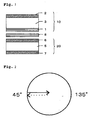
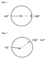
- Figs. 2 through 4 show a concept of polarizing conversion using a liquid crystal display which emits linear polarized light which is at an angle of 45 degrees in cross section on the equator on the Poincaré sphere, wherein the equator expresses a linear polarization condition in each direction of oscillations while the center (the north pole or the south pole) expresses a circular polarization condition.
- Fig. 2 represents the case where the direction of the orientation axes of a ⁇ /4-plate and a phase retarder are perpendicular to each other, Fig.
- Fig. 3 represents the case where the direction of the orientation axes of the ⁇ /4-plate and the phase retarder are parallel to each other
- Fig. 4 represents the case where the direction of the orientation axes of the ⁇ /4-plate and the phase retarder are shifted 45 degrees or less
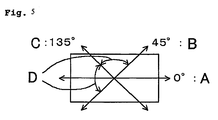
- Fig. 5 is a drawing which shows an example of a preferable angular arrangement for a polarizing plate, a phase retarder and an upper polarizing plate of a liquid crystal display where the direction of the orientation axis (optical axis) of a ⁇ /4-plate is in the direction of 0 degrees in the present invention.
- a ⁇ /4-plate 1 and a polarizing plate 2 are combined with each other so that the direction of their optical axes is at about 45 degrees relative to each other, whereby a circular polarizing plate is formed.
- the circular polarizing plate functions as an anti-reflection filter which efficiently absorbs internal reflection which is caused by incident light from outside.
- the circular polarizing plate is disposed separately as shown in Fig. 1 .
- the ⁇ /4-plate 1, the polarizing plate 2 and the transparent protection plate 3 form a laminated protection panel 10.
- a liquid crystal display 20 is usually formed of a liquid crystal display cell 5, an upper polarizing plate 6 and a lower polarizing plate 7 wherein these polarizing plates are arranged to the both surfaces of the liquid crystal display cell 5, the upper polarizing plate 6 may be omitted. It is preferable to omit the upper polarizing plate 6 if the brightness is regarded important, whereas it is preferable to have the upper polarizing plate 6 if the contrast is regarded as important.
- the polarizing plate 2 can be used those usually available in the field of liquid crystal displays. It is preferable to use, for instance, a uni-axially oriented film or the like, which is made by absorbing a dichroic material such as iodine and a dichroic dye in a polyvinylalcohol resin and orienting. In a normal use, protection films are stacked upon the both surfaces of a uni-axially oriented film in which a dichroic material is absorbed and oriented. Protection films are also similarly stacked on each of the upper polarizing plate 6 and the lower polarizing plate 7, which form the liquid crystal display 20.
- a uni-axially oriented film or the like which is made by absorbing a dichroic material such as iodine and a dichroic dye in a polyvinylalcohol resin and orienting.
- protection films are stacked upon the both surfaces of a uni-axially oriented film in which a dichroic material is absorbed and oriented.
- a phase retarder 8 whose wavelength dispersion is a specified value ⁇ B due to a relationship with the ⁇ /4-plate 1 is disposed between the laminated protection panel 10 and the liquid crystal display 20.
- the phase retarder 8 only needs to be between the laminated protection panel 10 and the liquid crystal display 20, and therefore, may be adhered to the back of the laminated protection panel 10 or to the front of the liquid crystal display 20, or alternatively, simply placed between the two. However, it is preferable to adhere to the front of the liquid crystal display 20, considering an anti-reflection effect.
- the transparent protection plate 3 is disposed below the polarizing plate 2, the transparent protection plate 3 is preferably made of an optically isotropic material, which is suitably glass, a polymeric film not oriented, etc. Further, the transparent protection plate 3 may be a touch panel. If the touch panel is a touch panel of the resistive membrane type, the ⁇ /4-plate 1, the polarizing plate 2 and the like may directly form a resistive membrane so as to serve also as an element which forms the touch panel.
- the phase retarder 8 is disposed between the laminated protection panel 10 and the liquid crystal display 20 so that displaying light from the liquid crystal display 20 is efficiently transmitted through the laminated protection panel 10 which comprises a transparent protection plate 3 and a circular polarizing plate which is formed by the ⁇ /4-plate 1 and the polarizing plate 2, wherein materials of the ⁇ /4-plate 1 and the phase retarder 8 is selected so that the sum ( ⁇ A + ⁇ B ) of the wavelength dispersion ⁇ A of the ⁇ /4-plate 1 which forms the laminated protection panel 10 and the wavelength dispersion ⁇ B of the phase retarder 8 ranges from 1.11 to 1.95, and the direction of the orientation axis of the phase retarder 8 may be within 0 ⁇ 45 degrees or 90 ⁇ 45 degrees with respect to the direction of the orientation axis of the /4-plate.
- the laminated protection panel 10 which comprises a transparent protection plate 3 and a circular polarizing plate which is formed by the ⁇ /4-plate 1 and the polarizing plate 2, wherein materials of the ⁇
- Oriented polymeric films are usually used as the /4-plate 1 and the phase retarder 8.
- Their wavelength dispersion values ⁇ A and ⁇ B are intrinsic to a material as described above, and hence, the materials of the ⁇ /4-plate 1 and the phase retarder 8 may be selected so as to satisfy the requirement above, that is, ( ⁇ A + ⁇ B ) is in the range of 1.11 to 1.95.
- a copolymer film its wavelength dispersion value ⁇ can be controlled by the copolymerization ratio of components. Accordingly, many kinds of copolymer film are applicable to the present invention.
- FIG. 2 A concept of polarizing conversion using a liquid crystal display which emits linear polarized light which is at 45 degrees, if described using the Poincaré sphere (a spherical surface in which each point on the sphere shows a state of polarization), is illustrated as shown in Figs. 2 through 4 .
- These drawings show the Poincaré sphere as a projection upon a cross section, which is on the equator.
- the solid arrows denote conversion by the phase retarder 8
- the dotted arrows denote conversion by the ⁇ /4-plate 1. Where two ⁇ /4-plates are arranged perpendicular to each other, the original condition of polarization is realized through the same trajectory as shown in Fig. 2 .
- polarizing conversion occur into a different direction by the different combination of the directions of the orientation axes of the phase retarder 8 and the ⁇ /4-plate 1.
- dispersion of the three primary colors of red, green and blue is prevented by such combination of the ⁇ /4-plate 1 and the phase retarder 8 so that ( ⁇ A + ⁇ B ) is in the range of 1.11 to 1. 95.
- the ⁇ /4-plate 1 and the phase retarder 8 are arranged so that their orientation axes are parallel to each other, conversion occurs as shown in Fig. 3 .
- Fig. 5 shows an example of a preferable angular arrangement for the polarizing plate 2, the phase retarder 8 and the upper polarizing plate 6 of the liquid crystal display 20 when the direction of the orientation axis (optical axis) of the ⁇ /4-plate 1 is in the direction of 0 degree.
- the polarizing plate 2, which forms the circular polarizing plate together with the ⁇ /4-plate 1, is disposed at an angle of 45 degrees with respect to the direction of the optical axis (A) of the ⁇ /4-plate 1.
- the upper polarizing plate 6 of the liquid crystal display is arranged to have its optical axis (absorption axis) (C) at an angle of 135 degrees with respect to the direction of the long side of the liquid crystal display, so that linear polarized light is emitted at angle of 45 degrees.
- the directions of the optical axis (B) of the polarizing plate 2 and the optical axis (C) of the upper polarizing plate 6 may be opposite to Fig. 5 , that is, the optical axis of the polarizing plate 2 may be at an angle of 135 degrees and the optical axis of the upper polarizing plate 6 may be at angle of 45 degrees.
- the phase retarder 8 is disposed so that its optical axis (D) is parallel to the optical axis (A) of the ⁇ /4-plate 1, or is perpendicular to the optical axis, is at an angle within ⁇ 45 degrees from the direction parallel to the optical axis, or is at an angle within ⁇ 45 degrees from the direction perpendicular to the optical axis. If the direction of the optical axis (D) of the phase retarder 8 is shifted to a certain extent from the direction of the optical axis (A) of the ⁇ /4-plate 1, as described earlier, the angle at which the ⁇ /4-plate 1 is disposed is slightly rotated, in this case, the optical axis of the polarizing plate 2 as well is correspondingly rotated. The optical axis of the upper polarizing plate 6 may change.
- a surface of the laminated protection panel 10 may have an additional function.
- a transparent hard coat layer for prevention of scratching may be disposed to the surface.
- the hard coat layer may be formed with applying a hard coat agent or adhering a hard coat film.
- an anti-glare layer may be formed which irregularly reflects external light by means of fine irregular patterns at the surface, or an anti-reflection layer may be formed which is a layer of a number of dielectric thin films.
- a transparent hard coat film in which anti-reflection layer is formed may be adhered, or alternatively, anti-reflection layer may be formed on a hard coat layer.
- a touch-panel type liquid crystal display device not according to the invention which comprises an isotropic touch panel of the resistive membrane type as a transparent protection plate and has the layer structure which includes (polarizing plate 2) / ( ⁇ /4-plate 1) / (touch panel 4) / (phase retarder 8) / (liquid crystal display 20).
- Retardation values in the examples not according to the invention are values at a wavelength of 550 nm.
- the measurement of luminance was conducted using a photometer MCPD manufactured by Otsuka Electronics Co.,Ltd.
- a polynorbornene film (under the trade name of "Artone” available from JSR Corporation) was uniaxially oriented, thereby obtaining the ⁇ /4-plate 1 whose wavelength dispersion ⁇ A was 1.00 and retardation value was 138 nm.
- the ⁇ /4-plate 1 and the polarizing plate 2 (under the trade name of SUMIKALAN SQW852A available from Sumitomo Chemical Co., Ltd.) were adhered to each other such that the direction of the orientation axis of the ⁇ /4-plate 1 was at 0 degree and the direction of the absorption axis of the polarizing plate 2 was at 45 degrees, and the obtained laminate was adhered, with the ⁇ /4-plate 1 facing down, on a top surface of the isotropic touch panel 4 of the resistive membrane type, whereby a touch panel with a circular polarizing plate was obtained.
- phase retarder 8 whose wavelength dispersion ⁇ was 0.93 and retardation value was 110 nm.
- the phase retarder 8 was adhered to a back surface of the touch panel above with the circular polarizing plate so that the direction of the orientation axis of the phase retarder 8 was at 0 degree.
- the touch panel 4 now laminating the circular polarizing plate adhered to the top surface and the phase retarder 8 adhered to the bottom surface was disposed on the liquid crystal display 20 in which the direction of the absorption axis of the upper polarizing plate 6 was at 135 degrees, in such a manner that the phase retarder 8 and the upper polarizing plate 6 were in contact, whereby the touch-panel type liquid crystal display device was obtained.
- the phase retarder 8 (under the trade name of "Pure Ace WR W-142" available from Teijin Limited) whose wavelength dispersion ⁇ B was 0.83 and retardation value was 138 nm was adhered to the surface of the liquid crystal display 20 in which the direction of the absorption axis of the upper polarizing plate 6 was at 135 degrees, in such a manner that the direction of the orientation axis of the phase retarder 8 was at 0 degree.
- the touch panel with a circular polarizing plate similar to the above in Example 1 not according to the invention was disposed on the phase retarder 8 side (the upper side) so that the direction of the orientation axis of the ⁇ /4-plate 1 was at 0 degree, whereby the touch-panel type liquid crystal display device was obtained.
- the ⁇ /4-plate 1 obtained in Example 1 not according to the invention and the polarizing plate 2 were adhered to each other such that the direction of the orientation axis of the ⁇ /4-plate 1 was at 0 degree and the direction of the absorption axis of the polarizing plate 2 was at 135 degrees, and the obtained laminate was adhered, with the ⁇ /4-plate 1 facing down, on a top surface of the isotropic touch panel 4 of the resistive membrane type, whereby the touch panel 11 with a circular polarizing plate was obtained.
- phase retarder 8 under the trade name of "Pure Ace WR W-142" available from Teijin Limited
- wavelength dispersion ⁇ B was 0.83 and retardation value was 138 nm was adhered to the surface of the liquid crystal display 20 in which the direction of the absorption axis of the upper polarizing plate 6 was at 135 degrees, in such a manner that the direction of the orientation axis of the phase retarder 8 was at 90 degrees.
- the bottom surface of the touch panel with the circular polarizing plate (the touch panel side) was disposed on the top surface of the liquid crystal display 20 with the phase retarder (the phase retarder side), whereby the touch-panel type liquid crystal display device was obtained.
- the ⁇ /4-plate 1 obtained in Example 1 not according to the invention and the polarizing plate 2 were adhered to each other such that the direction of the orientation axis of the ⁇ /4-plate 1 was at 0 degree and the direction of the absorption axis of the polarizing plate 2 was at 135 degrees, and the obtained laminate was adhered, with the ⁇ /4-plate 1 facing down, on a top surface of the isotropic touch panel 4 of the resistive membrane type, whereby the touch panel with a circular polarizing plate was obtained.
- phase retarder made of polycarbonate (under the trade name of "SEF340138B” available from Sumitomo Chemical Co., Ltd.) whose wavelength dispersion ⁇ B was 1.07 and retardation value was 138 nm, was adhered to the surface of the liquid crystal display 20 in which the direction of the absorption axis of the upper polarizing plate 6 was at 135 degrees, in such a manner that the direction of the orientation axis of the phase retarder was at 90 degrees.
- the bottom surface of the touch panel with the circular polarizing plate (the touch panel side) was disposed on the top surface of the liquid crystal display 20 with the phase retarder 8 (the phase retarder side), whereby the touch-panel type liquid crystal display device was obtained.
- Example 4 The same phase retarder as that used in Example 4 not according to the invention was used as the ⁇ /4-plate 1, and the ⁇ /4-plate 1 and the polarizing plate 2 were adhered to each other such that the direction of the orientation axis of the ⁇ /4-plate 1 was at 0 degree and the direction of the absorption axis of the polarizing plate 2 was at 45 degrees, and the obtained laminate was adhered, with the ⁇ /4-plate 1 facing down, on a top surface of the isotropic touch panel 4 of the resistive membrane type, whereby the touch panel with a circular polarizing plate was obtained.
- Example 4 another same phase ratarder as that used in Example 4 not according to the invention was adhered to the surface of the liquid crystal display 20 in which the direction of the absorption axis of the upper polarizing plate 6 was at 135 degrees, in such a manner that the direction of the orientation axis of the phase retarder was at 0 degree.
- the bottom surface of the touch panel with the circular polarizing plate (the touch panel side) was disposed on the top surface of the liquid crystal display 20 with the phase retarder 8 (the phase retarder side), whereby the touch-panel type liquid crystal display device was obtained.
- Table 1 Luminance levels in the respective examples not according to the invention are conversion values when the front luminance in Example 1 not according to the invention is assumed to be 100%.
- ⁇ A + ⁇ B Axial Angle of Phase retarder Direction of Evaluation Luminance Displayed view 435nm 545nm 612 nm
- Example 1 not according to the invention 1.93 0° Front 98% 98% 92% excellent at 40° to the right 67% 57% 51% excellent
- Example 2 not according to the invention 1.83 0° Front 98% 100% 98% excellent at 40° to the right 71% 68% 63% excellent
- Example 3 not according to the invention 1.83 90° Front 99% 100% 101% excellent at 40° to the right 76% 66% 67% excellent
- Example 5 not according to the invention 2.14 0° Front 59% 100% 98% yellowish at 40° to the right 66% 57% 49% excellent
- Example 4 while a displayed view from the front was excellent, a displayed view from the side was colored yellowish.
- Example 5 although a displayed view from the side was not yellowish, a displayed view from the front was yellowish, and therefore, this was not suitable as a display device. Unlike these, in Example 1 not according to the invention, a displayed view from the front was slightly bluish but only to such an extent that did not cause a concern, and a displayed view from the side was excellent without getting colored in yellow.
- Examples 2 and 3 not according to the invention both a displayed view from the front and a displayed view from the side were further improved, providing a wide viewing angle.
- the present invention provides a liquid crystal display device which is equipped with an anti-reflection function, excellent in visibility, and adaptable to the touch panel type and the like, and further, improves in viewing angle characteristic.
Landscapes
- Physics & Mathematics (AREA)
- Nonlinear Science (AREA)
- Mathematical Physics (AREA)
- Chemical & Material Sciences (AREA)
- Crystallography & Structural Chemistry (AREA)
- General Physics & Mathematics (AREA)
- Optics & Photonics (AREA)
- Liquid Crystal (AREA)
- Polarising Elements (AREA)
- Liquid Crystal Substances (AREA)
- Position Input By Displaying (AREA)
Applications Claiming Priority (4)
| Application Number | Priority Date | Filing Date | Title |
|---|---|---|---|
| JP2000262674 | 2000-08-31 | ||
| JP2000262674 | 2000-08-31 | ||
| JP2001032041 | 2001-02-08 | ||
| JP2001032041A JP2002148592A (ja) | 2000-08-31 | 2001-02-08 | 液晶表示装置 |
Publications (3)
| Publication Number | Publication Date |
|---|---|
| EP1184713A2 EP1184713A2 (en) | 2002-03-06 |
| EP1184713A3 EP1184713A3 (en) | 2004-03-31 |
| EP1184713B1 true EP1184713B1 (en) | 2008-02-20 |
Family
ID=26598916
Family Applications (1)
| Application Number | Title | Priority Date | Filing Date |
|---|---|---|---|
| EP01307161A Expired - Lifetime EP1184713B1 (en) | 2000-08-31 | 2001-08-23 | Liquid crystal display device |
Country Status (5)
| Country | Link |
|---|---|
| US (1) | US6738117B2 (enExample) |
| EP (1) | EP1184713B1 (enExample) |
| JP (1) | JP2002148592A (enExample) |
| AT (1) | ATE386959T1 (enExample) |
| DE (1) | DE60132857T2 (enExample) |
Families Citing this family (22)
| Publication number | Priority date | Publication date | Assignee | Title |
|---|---|---|---|---|
| KR100872476B1 (ko) * | 2002-07-10 | 2008-12-05 | 삼성전자주식회사 | 평판 표시 장치 |
| US7274418B2 (en) * | 2003-10-21 | 2007-09-25 | Symbol Technologies, Inc. | Method and system for improving the contrast of LCDs using circular polarization |
| US7209126B2 (en) * | 2003-12-23 | 2007-04-24 | Symbol Technologies, Inc. | Viewing angle-controlled displays for point-of-sale terminals and methods for fabricating the same |
| JP4060313B2 (ja) * | 2004-01-28 | 2008-03-12 | シャープ株式会社 | 表示装置 |
| WO2008066157A1 (en) * | 2006-11-30 | 2008-06-05 | Nippon Steel Chemical Co., Ltd. | Polarizing plate protective film, polarizing plate, and resistive touch panel |
| WO2008078812A1 (ja) * | 2006-12-27 | 2008-07-03 | Gunze Limited | 偏光板保護フィルム、偏光板及び抵抗膜式タッチパネル |
| JP5027086B2 (ja) * | 2008-09-25 | 2012-09-19 | 株式会社ジャパンディスプレイウェスト | 入力装置および入力機能付き表示装置 |
| JP2011252934A (ja) | 2008-09-25 | 2011-12-15 | Sharp Corp | 表示装置 |
| JP2010165032A (ja) | 2009-01-13 | 2010-07-29 | Hitachi Displays Ltd | タッチパネルディスプレイ装置 |
| KR101323434B1 (ko) * | 2009-06-08 | 2013-10-29 | 엘지디스플레이 주식회사 | 유기전계발광표시장치 |
| JP2012093985A (ja) * | 2010-10-27 | 2012-05-17 | Nitto Denko Corp | タッチ入力機能を有する表示パネル装置と該表示パネル装置のための光学ユニット、並びにその製造方法 |
| KR20120044041A (ko) * | 2010-10-27 | 2012-05-07 | 삼성모바일디스플레이주식회사 | 표시 장치 |
| KR101772079B1 (ko) * | 2011-03-28 | 2017-08-28 | 엘지전자 주식회사 | 터치스크린 패널 및 그 제조 방법 |
| JP2012220853A (ja) * | 2011-04-12 | 2012-11-12 | Keiwa Inc | メガネ用位相差フィルム、3dメガネ用光学シート及び3dメガネ |
| JP2013054271A (ja) * | 2011-09-06 | 2013-03-21 | Nissan Motor Co Ltd | 表示装置、自動車用表示装置、及び表示装置の製造方法 |
| US9158143B2 (en) * | 2011-09-12 | 2015-10-13 | Apple Inc. | Dual purpose touch sensor panel and optical retarder |
| JP2014219667A (ja) * | 2013-04-04 | 2014-11-20 | 日東電工株式会社 | 導電性フィルムおよび画像表示装置 |
| KR101444132B1 (ko) * | 2013-11-20 | 2014-11-04 | 동우 화인켐 주식회사 | 복합 편광판 일체형 터치 감지 전극 및 이를 구비한 터치 스크린 패널 |
| KR101629943B1 (ko) * | 2014-02-21 | 2016-06-13 | 주식회사 엘지화학 | 전자 칠판 |
| CN106374053B (zh) * | 2016-11-22 | 2018-05-25 | 上海天马微电子有限公司 | 一种oled显示面板和显示装置 |
| CN116339005A (zh) * | 2021-12-22 | 2023-06-27 | 鸿通科技(厦门)有限公司 | 显示装置 |
| TWI795147B (zh) * | 2021-12-27 | 2023-03-01 | 大陸商鴻通科技(廈門)有限公司 | 顯示裝置 |
Citations (1)
| Publication number | Priority date | Publication date | Assignee | Title |
|---|---|---|---|---|
| JP2000137116A (ja) * | 1998-10-30 | 2000-05-16 | Teijin Ltd | 位相差板及びそれを用いた液晶表示装置 |
Family Cites Families (17)
| Publication number | Priority date | Publication date | Assignee | Title |
|---|---|---|---|---|
| JPH05127822A (ja) | 1991-10-30 | 1993-05-25 | Daicel Chem Ind Ltd | タツチパネル |
| US6133980A (en) * | 1995-10-30 | 2000-10-17 | Metrologic Instruments, Inc. | Liquid crystal film structures with phase-retardation surface regions formed therein and methods of fabricating the same |
| US5657140A (en) * | 1993-12-15 | 1997-08-12 | Ois Optical Imaging Systems, Inc. | Normally white twisted nematic LCD with positive and negative retarders |
| US5999240A (en) * | 1995-05-23 | 1999-12-07 | Colorlink, Inc. | Optical retarder stack pair for transforming input light into polarization states having saturated color spectra |
| US5929946A (en) * | 1995-05-23 | 1999-07-27 | Colorlink, Inc. | Retarder stack for preconditioning light for a modulator having modulation and isotropic states of polarization |
| US5743980A (en) * | 1996-05-02 | 1998-04-28 | Industrial Technology Research Institute | Method of fabricating an optical retardation film |
| JPH1048625A (ja) | 1996-08-02 | 1998-02-20 | Sumitomo Chem Co Ltd | 液晶ディスプレイ用タッチパネル |
| US6208396B1 (en) * | 1996-10-25 | 2001-03-27 | Sumitomo Chemical Company, Limited | Normally white mode twisted nematic liquid crystal display device having improved viewing angle characteristics |
| JP3854392B2 (ja) * | 1996-11-11 | 2006-12-06 | 同和鉱業株式会社 | 光学的フィルター |
| US6147741A (en) * | 1997-02-25 | 2000-11-14 | Motorola, Inc. | Digital scanner employing recorded phase information and method of fabrication |
| JP2000112663A (ja) * | 1997-11-27 | 2000-04-21 | Kanegafuchi Chem Ind Co Ltd | 透明タッチパネルおよび透明タッチパネル付液晶セル |
| JP4211088B2 (ja) * | 1998-06-16 | 2009-01-21 | 凸版印刷株式会社 | 防眩性ハードコートフィルムもしくはシート |
| JP3690125B2 (ja) * | 1998-07-23 | 2005-08-31 | 住友化学株式会社 | 液晶表示装置 |
| DE69928759T2 (de) * | 1998-08-04 | 2006-06-29 | Kaneka Corp. | Flüssigkristallanzeigevorrichtung mit berührungsschirm |
| JP2000206531A (ja) * | 1999-01-14 | 2000-07-28 | Kanegafuchi Chem Ind Co Ltd | タッチパネル付き液晶表示装置及びタッチパネル |
| JP2000111896A (ja) * | 1998-08-04 | 2000-04-21 | Kanegafuchi Chem Ind Co Ltd | タッチパネル付き液晶表示装置及びタッチパネル |
| JP4592862B2 (ja) | 1999-09-03 | 2010-12-08 | グンゼ株式会社 | タッチパネル |
-
2001
- 2001-02-08 JP JP2001032041A patent/JP2002148592A/ja active Pending
- 2001-08-15 US US09/929,067 patent/US6738117B2/en not_active Expired - Lifetime
- 2001-08-23 EP EP01307161A patent/EP1184713B1/en not_active Expired - Lifetime
- 2001-08-23 DE DE60132857T patent/DE60132857T2/de not_active Expired - Lifetime
- 2001-08-23 AT AT01307161T patent/ATE386959T1/de not_active IP Right Cessation
Patent Citations (1)
| Publication number | Priority date | Publication date | Assignee | Title |
|---|---|---|---|---|
| JP2000137116A (ja) * | 1998-10-30 | 2000-05-16 | Teijin Ltd | 位相差板及びそれを用いた液晶表示装置 |
Also Published As
| Publication number | Publication date |
|---|---|
| JP2002148592A (ja) | 2002-05-22 |
| EP1184713A2 (en) | 2002-03-06 |
| DE60132857D1 (de) | 2008-04-03 |
| DE60132857T2 (de) | 2009-02-12 |
| US6738117B2 (en) | 2004-05-18 |
| US20020047969A1 (en) | 2002-04-25 |
| EP1184713A3 (en) | 2004-03-31 |
| ATE386959T1 (de) | 2008-03-15 |
Similar Documents
| Publication | Publication Date | Title |
|---|---|---|
| EP1184713B1 (en) | Liquid crystal display device | |
| EP4325281A2 (en) | Directional display apparatus | |
| JP3854392B2 (ja) | 光学的フィルター | |
| JP3337028B2 (ja) | 液晶装置及び電子機器 | |
| US8208097B2 (en) | Color compensation multi-layered member for display apparatus, optical filter for display apparatus having the same and display apparatus having the same | |
| EP1679545A1 (en) | Privacy screen for a display | |
| JP3058620B2 (ja) | 液晶表示装置 | |
| KR20120112063A (ko) | 표시 장치 및 전자 기기 | |
| JP2005173571A (ja) | ディスプレイ用プライバシーフィルタ | |
| US20180321546A1 (en) | Switching mirror panel and switching mirror device | |
| WO2019103012A1 (ja) | 表示装置 | |
| CN101363929B (zh) | 用于显示装置的色彩补偿多层构件和滤光片以及显示装置 | |
| US8040475B2 (en) | Reflective morphable display device and method of feature activation | |
| JP3345772B2 (ja) | 液晶装置及び電子機器 | |
| CN100520524C (zh) | 液晶显示装置 | |
| US20070236630A1 (en) | Liquid crystal display device | |
| US20050112342A1 (en) | Privacy screen for a display | |
| JPH1164631A (ja) | 偏光手段及び液晶装置及び電子機器 | |
| JP2002072214A (ja) | 液晶表示用装置 | |
| US8810753B2 (en) | Liquid crystal device and electronic apparatus | |
| JP3760656B2 (ja) | 液晶装置及び電子機器 | |
| JPH11142646A (ja) | 反射偏光子、液晶装置及び電子機器 | |
| JP3389924B2 (ja) | 液晶装置及び電子機器 | |
| JP3337029B2 (ja) | 液晶装置及び電子機器 | |
| CN113433728A (zh) | 一种基于双向反射功能层补偿的一体黑设备 |
Legal Events
| Date | Code | Title | Description |
|---|---|---|---|
| PUAI | Public reference made under article 153(3) epc to a published international application that has entered the european phase |
Free format text: ORIGINAL CODE: 0009012 |
|
| AK | Designated contracting states |
Kind code of ref document: A2 Designated state(s): AT BE CH CY DE DK ES FI FR GB GR IE IT LI LU MC NL PT SE TR |
|
| AX | Request for extension of the european patent |
Free format text: AL;LT;LV;MK;RO;SI |
|
| PUAL | Search report despatched |
Free format text: ORIGINAL CODE: 0009013 |
|
| AK | Designated contracting states |
Kind code of ref document: A3 Designated state(s): AT BE CH CY DE DK ES FI FR GB GR IE IT LI LU MC NL PT SE TR |
|
| AX | Request for extension of the european patent |
Extension state: AL LT LV MK RO SI |
|
| RIC1 | Information provided on ipc code assigned before grant |
Ipc: 7G 02F 1/133 A Ipc: 7G 02F 1/13363B Ipc: 7G 02B 5/30 B |
|
| 17P | Request for examination filed |
Effective date: 20040913 |
|
| AKX | Designation fees paid |
Designated state(s): AT BE CH CY DE DK ES FI FR GB GR IE IT LI LU MC NL PT SE TR |
|
| RAP1 | Party data changed (applicant data changed or rights of an application transferred) |
Owner name: SUMITOMO CHEMICAL COMPANY, LIMITED |
|
| 17Q | First examination report despatched |
Effective date: 20041119 |
|
| GRAP | Despatch of communication of intention to grant a patent |
Free format text: ORIGINAL CODE: EPIDOSNIGR1 |
|
| GRAS | Grant fee paid |
Free format text: ORIGINAL CODE: EPIDOSNIGR3 |
|
| GRAA | (expected) grant |
Free format text: ORIGINAL CODE: 0009210 |
|
| AK | Designated contracting states |
Kind code of ref document: B1 Designated state(s): AT BE CH CY DE DK ES FI FR GB GR IE IT LI LU MC NL PT SE TR |
|
| REG | Reference to a national code |
Ref country code: GB Ref legal event code: FG4D |
|
| REG | Reference to a national code |
Ref country code: CH Ref legal event code: EP |
|
| REG | Reference to a national code |
Ref country code: IE Ref legal event code: FG4D |
|
| REF | Corresponds to: |
Ref document number: 60132857 Country of ref document: DE Date of ref document: 20080403 Kind code of ref document: P |
|
| REG | Reference to a national code |
Ref country code: SE Ref legal event code: TRGR |
|
| PG25 | Lapsed in a contracting state [announced via postgrant information from national office to epo] |
Ref country code: ES Free format text: LAPSE BECAUSE OF FAILURE TO SUBMIT A TRANSLATION OF THE DESCRIPTION OR TO PAY THE FEE WITHIN THE PRESCRIBED TIME-LIMIT Effective date: 20080531 |
|
| PG25 | Lapsed in a contracting state [announced via postgrant information from national office to epo] |
Ref country code: AT Free format text: LAPSE BECAUSE OF FAILURE TO SUBMIT A TRANSLATION OF THE DESCRIPTION OR TO PAY THE FEE WITHIN THE PRESCRIBED TIME-LIMIT Effective date: 20080220 |
|
| PG25 | Lapsed in a contracting state [announced via postgrant information from national office to epo] |
Ref country code: BE Free format text: LAPSE BECAUSE OF FAILURE TO SUBMIT A TRANSLATION OF THE DESCRIPTION OR TO PAY THE FEE WITHIN THE PRESCRIBED TIME-LIMIT Effective date: 20080220 |
|
| ET | Fr: translation filed | ||
| PG25 | Lapsed in a contracting state [announced via postgrant information from national office to epo] |
Ref country code: PT Free format text: LAPSE BECAUSE OF FAILURE TO SUBMIT A TRANSLATION OF THE DESCRIPTION OR TO PAY THE FEE WITHIN THE PRESCRIBED TIME-LIMIT Effective date: 20080721 Ref country code: DK Free format text: LAPSE BECAUSE OF FAILURE TO SUBMIT A TRANSLATION OF THE DESCRIPTION OR TO PAY THE FEE WITHIN THE PRESCRIBED TIME-LIMIT Effective date: 20080220 |
|
| PLBE | No opposition filed within time limit |
Free format text: ORIGINAL CODE: 0009261 |
|
| STAA | Information on the status of an ep patent application or granted ep patent |
Free format text: STATUS: NO OPPOSITION FILED WITHIN TIME LIMIT |
|
| 26N | No opposition filed |
Effective date: 20081121 |
|
| PG25 | Lapsed in a contracting state [announced via postgrant information from national office to epo] |
Ref country code: MC Free format text: LAPSE BECAUSE OF NON-PAYMENT OF DUE FEES Effective date: 20080831 |
|
| REG | Reference to a national code |
Ref country code: CH Ref legal event code: PL |
|
| PG25 | Lapsed in a contracting state [announced via postgrant information from national office to epo] |
Ref country code: LI Free format text: LAPSE BECAUSE OF NON-PAYMENT OF DUE FEES Effective date: 20080831 Ref country code: CH Free format text: LAPSE BECAUSE OF NON-PAYMENT OF DUE FEES Effective date: 20080831 |
|
| PG25 | Lapsed in a contracting state [announced via postgrant information from national office to epo] |
Ref country code: CY Free format text: LAPSE BECAUSE OF FAILURE TO SUBMIT A TRANSLATION OF THE DESCRIPTION OR TO PAY THE FEE WITHIN THE PRESCRIBED TIME-LIMIT Effective date: 20080220 Ref country code: IE Free format text: LAPSE BECAUSE OF NON-PAYMENT OF DUE FEES Effective date: 20080825 |
|
| PG25 | Lapsed in a contracting state [announced via postgrant information from national office to epo] |
Ref country code: LU Free format text: LAPSE BECAUSE OF NON-PAYMENT OF DUE FEES Effective date: 20080823 |
|
| PG25 | Lapsed in a contracting state [announced via postgrant information from national office to epo] |
Ref country code: TR Free format text: LAPSE BECAUSE OF FAILURE TO SUBMIT A TRANSLATION OF THE DESCRIPTION OR TO PAY THE FEE WITHIN THE PRESCRIBED TIME-LIMIT Effective date: 20080220 |
|
| PG25 | Lapsed in a contracting state [announced via postgrant information from national office to epo] |
Ref country code: GR Free format text: LAPSE BECAUSE OF FAILURE TO SUBMIT A TRANSLATION OF THE DESCRIPTION OR TO PAY THE FEE WITHIN THE PRESCRIBED TIME-LIMIT Effective date: 20080521 |
|
| PGFP | Annual fee paid to national office [announced via postgrant information from national office to epo] |
Ref country code: GB Payment date: 20110817 Year of fee payment: 11 Ref country code: FR Payment date: 20110818 Year of fee payment: 11 Ref country code: SE Payment date: 20110811 Year of fee payment: 11 Ref country code: FI Payment date: 20110810 Year of fee payment: 11 |
|
| PGFP | Annual fee paid to national office [announced via postgrant information from national office to epo] |
Ref country code: NL Payment date: 20110818 Year of fee payment: 11 Ref country code: IT Payment date: 20110813 Year of fee payment: 11 |
|
| REG | Reference to a national code |
Ref country code: NL Ref legal event code: V1 Effective date: 20130301 |
|
| REG | Reference to a national code |
Ref country code: SE Ref legal event code: EUG |
|
| GBPC | Gb: european patent ceased through non-payment of renewal fee |
Effective date: 20120823 |
|
| PG25 | Lapsed in a contracting state [announced via postgrant information from national office to epo] |
Ref country code: NL Free format text: LAPSE BECAUSE OF NON-PAYMENT OF DUE FEES Effective date: 20130301 Ref country code: SE Free format text: LAPSE BECAUSE OF NON-PAYMENT OF DUE FEES Effective date: 20120824 Ref country code: FI Free format text: LAPSE BECAUSE OF NON-PAYMENT OF DUE FEES Effective date: 20120823 |
|
| REG | Reference to a national code |
Ref country code: FR Ref legal event code: ST Effective date: 20130430 |
|
| PG25 | Lapsed in a contracting state [announced via postgrant information from national office to epo] |
Ref country code: IT Free format text: LAPSE BECAUSE OF NON-PAYMENT OF DUE FEES Effective date: 20120823 |
|
| PG25 | Lapsed in a contracting state [announced via postgrant information from national office to epo] |
Ref country code: GB Free format text: LAPSE BECAUSE OF NON-PAYMENT OF DUE FEES Effective date: 20120823 |
|
| PG25 | Lapsed in a contracting state [announced via postgrant information from national office to epo] |
Ref country code: FR Free format text: LAPSE BECAUSE OF NON-PAYMENT OF DUE FEES Effective date: 20120831 |
|
| PGFP | Annual fee paid to national office [announced via postgrant information from national office to epo] |
Ref country code: DE Payment date: 20180807 Year of fee payment: 18 |
|
| REG | Reference to a national code |
Ref country code: DE Ref legal event code: R119 Ref document number: 60132857 Country of ref document: DE |
|
| PG25 | Lapsed in a contracting state [announced via postgrant information from national office to epo] |
Ref country code: DE Free format text: LAPSE BECAUSE OF NON-PAYMENT OF DUE FEES Effective date: 20200303 |