EP1183751B1 - Hf-schalter - Google Patents
Hf-schalter Download PDFInfo
- Publication number
- EP1183751B1 EP1183751B1 EP01908132A EP01908132A EP1183751B1 EP 1183751 B1 EP1183751 B1 EP 1183751B1 EP 01908132 A EP01908132 A EP 01908132A EP 01908132 A EP01908132 A EP 01908132A EP 1183751 B1 EP1183751 B1 EP 1183751B1
- Authority
- EP
- European Patent Office
- Prior art keywords
- strip line
- strip
- terminal
- diode
- coupled
- Prior art date
- Legal status (The legal status is an assumption and is not a legal conclusion. Google has not performed a legal analysis and makes no representation as to the accuracy of the status listed.)
- Expired - Lifetime
Links
Images


Classifications
-
- H—ELECTRICITY
- H01—ELECTRIC ELEMENTS
- H01P—WAVEGUIDES; RESONATORS, LINES, OR OTHER DEVICES OF THE WAVEGUIDE TYPE
- H01P1/00—Auxiliary devices
- H01P1/10—Auxiliary devices for switching or interrupting
-
- H—ELECTRICITY
- H01—ELECTRIC ELEMENTS
- H01P—WAVEGUIDES; RESONATORS, LINES, OR OTHER DEVICES OF THE WAVEGUIDE TYPE
- H01P1/00—Auxiliary devices
- H01P1/10—Auxiliary devices for switching or interrupting
- H01P1/15—Auxiliary devices for switching or interrupting by semiconductor devices
Definitions
- the present invention relates to a radio frequency (RF) switch used in an RF unit of various communication apparatuses.
- RF radio frequency
- a radio frequency (RF) switch causing a less insertion loss during transmission is provided.
- a strip line disposed in the RF switch is formed by a combination of two strip lines having different characteristic impedances from each other.
- the RF switch comprises:
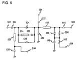
- Capacitor C 1 also prevents the capacity between the ends of diode D 1 from decreasing the characteristic impedance of strip line L at the receiving circuit 103 side when diode D 2 is turned off during the reception.
- the characteristic impedance of strip line L 2 at the receiving circuit 103 side is set higher than that of strip line L 1 at the antenna 101 side, the capacitance of capacitor C 1 can be reduced.
- the characteristic impedance of strip line L 1 is particularly set to substantially 50 ohms, compensating capacitor C 1 can be omitted.
- Capacitors C 2 at respective ends of antenna 101, transmitting circuit 102, and receiving circuit 103 cut a direct current (DC) component of the positive voltage applied from controller 104.
- DC direct current
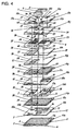
- the mounting electrode 25c side of chip diode 8, diode D 1 in Fig. 2, is coupled to connection electrode 33 through via hole 32, and to strip line 24, capacitor electrode 22, capacitor electrode 20, strip line 16, and capacitor electrode 15b through via hole 34.
- the mounting electrode 25d side of chip diode 8 is coupled to antenna terminal electrode 2 through via hole 35 and connection electrode 36. Electrode 36 is coupled to an end of strip line 17b through via hole 37.
- Strip lines 17a, 17b are connected through via hole 18. Because the electric characteristic of via hole 18, namely, Q value, is higher than that of an electrode pattern or the like formed on side surfaces of the layered product, the increasing of the insertion loss of the RF switch at this part is suppressed.
Landscapes
- Waveguide Switches, Polarizers, And Phase Shifters (AREA)
- Transceivers (AREA)
- Production Of Multi-Layered Print Wiring Board (AREA)
Claims (8)
- Hochfrequenzschalter zum selektiven Koppeln einer Antenne mit einer Sendeschaltung und einer Empfangsschaltung, der umfasst:einen ersten Anschluss (101), der zur Verbindung mit der Antenne eingerichtet ist;einen zweiten Anschluss (102), der zur Verbindung mit der Sendeschaltung eingerichtet ist;einen dritten Anschluss (103), der zur Verbindung mit der Empfangsschaltung eingerichtet ist;eine erste Diode (D1), die zwischen den ersten Anschluss und den zweiten Anschluss gekoppelt ist;eine Streifenleitung (L) von im Wesentlichen 1/4-Wellenlänge einer Sendefrequenz, die zwischen den ersten Anschluss und den dritten Anschluss gekoppelt ist;eine zweite Diode (D2), die zwischen den dritten Anschluss und Erde gekoppelt ist; undeine Steuerung (104), die Durchlass/Sperr-Schalten der ersten und der zweiten Diode steuert,dadurch gekennzeichnet, dass:die Streifenleitung (L) durch eine erste und eine zweite Streifenleitung (L1, L2) gebildet wird,die erste Streifenleitung (L1) mit einer Seite in Richtung des ersten Anschlusses gekoppelt ist,die zweite Streifenleitung (L2) mit einer Seite in Richtung des dritten Anschlusses gekoppelt ist, undeine charakteristische Impedanz der zweiten Streifenleitung (L2) höher ist als eine charakteristische Impedanz der ersten Streifenleitung (L1).
- Hochfrequenzschalter nach Anspruch 1, wobei die charakteristische Impedanz der ersten Streifenleitung (L1) im Wesentlichen 50 Ohm beträgt.
- Hochfrequenzschalter nach einem der Ansprüche 1 bis 2, der des Weiteren umfasst:einen geschichteten Körper (1), der ausgebildet wird, indem eine Vielzahl dielektrischer Scheiben (10a - 10k) geschichtet werden; undeine Erdungselektrode (6), die in dem geschichteten Körper (1) angeordnet ist,wobei die erste Diode (D1) auf dem geschichteten Körper (1) angeordnet ist,wobei die Streifenleitung (L) in dem geschichteten Körper (1) angeordnet ist,wobei die zweite Diode (D2) auf dem geschichteten Körper (1) angeordnet ist.
- Hochfrequenzschalter nach Anspruch 3, wobei sich die Leitungsbreiten der ersten und der zweiten Streifenleitung (L1, L2) voneinander unterscheiden.
- Hochfrequenzschalter nach Anspruch 3, wobei die erste (L1, 17b) und die zweite Streifenleitung (L2, 17a) jeweils auf verschiedenen dielektrischen Scheiben (10e, 10d) der dielektrischen Scheiben in dem geschichteten Körper (1) angeordnet sind.
- Hochfrequenzschalter nach Anspruch 3, wobei
sich Leitungsbreiten der ersten und der zweiten Streifenleitung (L1, L2) voneinander unterscheiden, und
die erste (L1, 17b) sowie die zweite Streifenleitung (L2, 17a) jeweils auf verschiedenen dielektrischen Scheiben (10e, 10d) der dielektrischen Scheiben in dem geschichteten Körper (1) angeordnet sind. - Hochfrequenzschalter nach Anspruch 3, wobei sich ein Abstand zwischen der ersten Streifenleitung (17b) und der Erdungselektrode (11c) von einem Abstand zwischen der zweiten Streifenleitung (17a) und der Erdungselektrode (11b) unterscheidet.
- Hochfrequenzschalter nach einem der Ansprüche 5 bis 7, wobei die erste (17b) und die zweite Streifenleitung (17a) jeweils auf verschiedenen dielektrischen Scheiben (10e, 10d) der dielektrischen Scheiben in dem geschichteten Körper (1) angeordnet und über ein Kontaktloch (18) miteinander gekoppelt sind.
Applications Claiming Priority (3)
| Application Number | Priority Date | Filing Date | Title |
|---|---|---|---|
| JP2000086150A JP3405316B2 (ja) | 2000-03-27 | 2000-03-27 | 高周波スイッチ |
| JP2000086150 | 2000-03-27 | ||
| PCT/JP2001/001492 WO2001073885A1 (en) | 2000-03-27 | 2001-02-28 | Rf switch |
Publications (2)
| Publication Number | Publication Date |
|---|---|
| EP1183751A1 EP1183751A1 (de) | 2002-03-06 |
| EP1183751B1 true EP1183751B1 (de) | 2006-04-26 |
Family
ID=18602363
Family Applications (1)
| Application Number | Title | Priority Date | Filing Date |
|---|---|---|---|
| EP01908132A Expired - Lifetime EP1183751B1 (de) | 2000-03-27 | 2001-02-28 | Hf-schalter |
Country Status (7)
| Country | Link |
|---|---|
| US (1) | US7123884B2 (de) |
| EP (1) | EP1183751B1 (de) |
| JP (1) | JP3405316B2 (de) |
| KR (1) | KR100719089B1 (de) |
| CN (1) | CN1186847C (de) |
| DE (1) | DE60119046T2 (de) |
| WO (1) | WO2001073885A1 (de) |
Families Citing this family (18)
| Publication number | Priority date | Publication date | Assignee | Title |
|---|---|---|---|---|
| JP3810011B2 (ja) * | 2003-08-08 | 2006-08-16 | Tdk株式会社 | 高周波スイッチモジュールおよび高周波スイッチモジュール用多層基板 |
| CN1315262C (zh) * | 2004-05-21 | 2007-05-09 | 粟毅 | 高频超宽带射频开关 |
| JP4379254B2 (ja) * | 2004-08-16 | 2009-12-09 | ソニー株式会社 | 分配器および通信方法 |
| KR100695969B1 (ko) | 2005-02-07 | 2007-03-15 | 알에프코어 주식회사 | Rf 스위치 및 rf 스위치를 구비하는 장치 |
| US7359677B2 (en) * | 2005-06-10 | 2008-04-15 | Sige Semiconductor Inc. | Device and methods for high isolation and interference suppression switch-filter |
| KR100864078B1 (ko) | 2005-11-08 | 2008-10-16 | 주식회사 케이엠더블유 | 고주파 스위치 |
| WO2007083861A1 (en) | 2006-01-20 | 2007-07-26 | Kmw Inc. | Radio frequency switch |
| US20070173210A1 (en) * | 2006-01-26 | 2007-07-26 | Lg Innotek Co., Ltd | Signal processing apparatus |
| KR100848261B1 (ko) * | 2007-02-05 | 2008-07-25 | 주식회사 이엠따블유안테나 | Rf 스위치 및 rf 스위치를 포함하는 장치 |
| US8005448B1 (en) * | 2007-05-10 | 2011-08-23 | Rf Micro Devices, Inc. | Radio frequency duplex filter for removing transmit signals from a receive path |
| CN102469681A (zh) * | 2010-11-17 | 2012-05-23 | 精英电脑股份有限公司 | 抑制噪声的线路布局结构 |
| US8638698B2 (en) * | 2011-07-26 | 2014-01-28 | Motorola Mobility Llc | Front end employing pin diode switch with high linearity and low loss for simultaneous transmission |
| US9306613B2 (en) | 2013-01-10 | 2016-04-05 | Google Technology Holdings LLC | Variable antenna match linearity |
| CN103746680B (zh) * | 2013-12-31 | 2017-01-25 | 北京朗波芯微技术有限公司 | 射频开关 |
| US10778206B2 (en) | 2018-03-20 | 2020-09-15 | Analog Devices Global Unlimited Company | Biasing of radio frequency switches for fast switching |
| US11152917B1 (en) | 2020-05-28 | 2021-10-19 | Analog Devices International Unlimited Company | Multi-level buffers for biasing of radio frequency switches |
| US11863227B2 (en) | 2021-10-25 | 2024-01-02 | Analog Devices International Unlimited Company | Radio frequency switches with fast switching speed |
| CN116938211A (zh) * | 2022-04-01 | 2023-10-24 | 深圳市晶准通信技术有限公司 | 射频开关电路、集成电路芯片及电子装置 |
Citations (1)
| Publication number | Priority date | Publication date | Assignee | Title |
|---|---|---|---|---|
| US5499000A (en) * | 1994-05-17 | 1996-03-12 | Murata Manufacturing Co., Ltd. | High-frequency switch |
Family Cites Families (19)
| Publication number | Priority date | Publication date | Assignee | Title |
|---|---|---|---|---|
| US4371853A (en) * | 1979-10-30 | 1983-02-01 | Matsushita Electric Industrial Company, Limited | Strip-line resonator and a band pass filter having the same |
| JPS5895403A (ja) * | 1981-12-01 | 1983-06-07 | Matsushita Electric Ind Co Ltd | 同軸型誘電体共振器 |
| DE3248246A1 (de) | 1982-12-28 | 1984-06-28 | Basf Ag, 6700 Ludwigshafen | Positiv arbeitendes verfahren zur herstellung von relief- und druckformen |
| JPS6139701A (ja) * | 1984-07-31 | 1986-02-25 | Nec Corp | 混成集積回路装置 |
| JPH02189001A (ja) | 1989-01-18 | 1990-07-25 | Nec Corp | Pinダイオードスイッチ |
| DE4222190A1 (de) * | 1992-07-07 | 1994-01-13 | Philips Patentverwaltung | Funkgerät mit einer Antennenumschaltvorrichtung |
| US5442812A (en) * | 1992-07-08 | 1995-08-15 | Matsushita Electric Industrial Co., Ltd. | Antenna switching apparatus for selectively connecting antenna to transmitter or receiver |
| US5507011A (en) * | 1992-12-22 | 1996-04-09 | Murata Manufacturing Co., Ltd. | High-frequency switch including strip line and two switching diodes |
| JP3307044B2 (ja) * | 1993-12-24 | 2002-07-24 | 松下電器産業株式会社 | 誘電体共振器およびその入出力結合回路 |
| KR0164368B1 (ko) * | 1995-10-25 | 1999-02-01 | 김광호 | 고주파 전력합성기 |
| JPH1032521A (ja) | 1996-07-17 | 1998-02-03 | Murata Mfg Co Ltd | デュプレクサ |
| JPH10135703A (ja) | 1996-10-29 | 1998-05-22 | Hitachi Metals Ltd | ダイオードスイッチ |
| JP3566024B2 (ja) | 1997-03-31 | 2004-09-15 | 三菱電機株式会社 | アンテナ給電回路 |
| JP3381547B2 (ja) | 1997-04-07 | 2003-03-04 | 三菱電機株式会社 | 高周波スイッチと送受信切替装置 |
| JP3644619B2 (ja) | 1997-06-25 | 2005-05-11 | 株式会社村田製作所 | 高周波伝送線路を有した電子部品 |
| JP3292095B2 (ja) | 1997-07-07 | 2002-06-17 | 株式会社村田製作所 | 高周波スイッチ |
| JPH11122139A (ja) * | 1997-10-17 | 1999-04-30 | Murata Mfg Co Ltd | アンテナ共用器 |
| ES2244845T3 (es) | 1997-12-03 | 2005-12-16 | Hitachi Metals, Ltd. | Modulo de continuacion multibanda de alta frecuencia. |
| JP3574893B2 (ja) * | 1999-10-13 | 2004-10-06 | 株式会社村田製作所 | 誘電体フィルタ、誘電体デュプレクサおよび通信装置 |
-
2000
- 2000-03-27 JP JP2000086150A patent/JP3405316B2/ja not_active Ceased
-
2001
- 2001-02-28 US US09/979,154 patent/US7123884B2/en not_active Expired - Fee Related
- 2001-02-28 CN CNB018006310A patent/CN1186847C/zh not_active Expired - Fee Related
- 2001-02-28 DE DE60119046T patent/DE60119046T2/de not_active Expired - Fee Related
- 2001-02-28 KR KR1020017014268A patent/KR100719089B1/ko not_active Expired - Fee Related
- 2001-02-28 WO PCT/JP2001/001492 patent/WO2001073885A1/en not_active Ceased
- 2001-02-28 EP EP01908132A patent/EP1183751B1/de not_active Expired - Lifetime
Patent Citations (1)
| Publication number | Priority date | Publication date | Assignee | Title |
|---|---|---|---|---|
| US5499000A (en) * | 1994-05-17 | 1996-03-12 | Murata Manufacturing Co., Ltd. | High-frequency switch |
Also Published As
| Publication number | Publication date |
|---|---|
| US7123884B2 (en) | 2006-10-17 |
| JP2001274722A (ja) | 2001-10-05 |
| US20020158705A1 (en) | 2002-10-31 |
| CN1186847C (zh) | 2005-01-26 |
| EP1183751A1 (de) | 2002-03-06 |
| WO2001073885A1 (en) | 2001-10-04 |
| KR100719089B1 (ko) | 2007-05-17 |
| JP3405316B2 (ja) | 2003-05-12 |
| DE60119046T2 (de) | 2006-08-31 |
| CN1365525A (zh) | 2002-08-21 |
| KR20020071717A (ko) | 2002-09-13 |
| DE60119046D1 (de) | 2006-06-01 |
Similar Documents
| Publication | Publication Date | Title |
|---|---|---|
| EP1183751B1 (de) | Hf-schalter | |
| US7391284B2 (en) | High-frequency switch | |
| US6759922B2 (en) | High directivity multi-band coupled-line coupler for RF power amplifier | |
| US5507011A (en) | High-frequency switch including strip line and two switching diodes | |
| JP3291913B2 (ja) | 高周波スイッチ | |
| EP1532745B1 (de) | Hochfrequenzmodul | |
| US7528678B2 (en) | Antenna Switch Module | |
| JPH07154110A (ja) | 伝送路共振器、及びこれを用いた無線周波数フィルタ | |
| GB2317271A (en) | Multiple or broad band antenna element arrangement for a portable radio | |
| EP1492245A1 (de) | Sende-Empfangsumschalter | |
| JP2002299922A (ja) | 高周波モジュール | |
| JP3186397B2 (ja) | 高周波スイッチ | |
| JP4239155B2 (ja) | ローパスフィルタ及びそれを用いた高周波スイッチ | |
| JP4172784B2 (ja) | 電圧制御可変フィルタおよび通信装置 | |
| JP3832484B2 (ja) | 高周波スイッチ | |
| JP2003078442A (ja) | 複合高周波部品 | |
| JP4751301B2 (ja) | 高周波スイッチ回路 | |
| JP2001345735A (ja) | 高周波スイッチ回路 | |
| JP2001345733A (ja) | 送受信制御回路 | |
| JP2004260624A (ja) | 送受信制御装置 | |
| JP2001144567A (ja) | 可変減衰器とこれを用いたagc回路 | |
| JPH1197901A (ja) | アンテナ切り替えスイッチ | |
| JP2006223004A (ja) | 高周波スイッチ |
Legal Events
| Date | Code | Title | Description |
|---|---|---|---|
| PUAI | Public reference made under article 153(3) epc to a published international application that has entered the european phase |
Free format text: ORIGINAL CODE: 0009012 |
|
| 17P | Request for examination filed |
Effective date: 20011122 |
|
| AK | Designated contracting states |
Kind code of ref document: A1 Designated state(s): AT BE CH CY DE DK ES FI FR GB GR IE IT LI LU MC NL PT SE TR |
|
| AX | Request for extension of the european patent |
Free format text: AL;LT;LV;MK;RO;SI |
|
| TPAC | Observations filed by third parties |
Free format text: ORIGINAL CODE: EPIDOSNTIPA |
|
| RBV | Designated contracting states (corrected) |
Designated state(s): DE FR GB |
|
| 17Q | First examination report despatched |
Effective date: 20040625 |
|
| GRAP | Despatch of communication of intention to grant a patent |
Free format text: ORIGINAL CODE: EPIDOSNIGR1 |
|
| GRAS | Grant fee paid |
Free format text: ORIGINAL CODE: EPIDOSNIGR3 |
|
| GRAA | (expected) grant |
Free format text: ORIGINAL CODE: 0009210 |
|
| AK | Designated contracting states |
Kind code of ref document: B1 Designated state(s): DE FR GB |
|
| REG | Reference to a national code |
Ref country code: GB Ref legal event code: FG4D |
|
| REF | Corresponds to: |
Ref document number: 60119046 Country of ref document: DE Date of ref document: 20060601 Kind code of ref document: P |
|
| ET | Fr: translation filed | ||
| PLBE | No opposition filed within time limit |
Free format text: ORIGINAL CODE: 0009261 |
|
| STAA | Information on the status of an ep patent application or granted ep patent |
Free format text: STATUS: NO OPPOSITION FILED WITHIN TIME LIMIT |
|
| 26N | No opposition filed |
Effective date: 20070129 |
|
| PGFP | Annual fee paid to national office [announced via postgrant information from national office to epo] |
Ref country code: DE Payment date: 20090226 Year of fee payment: 9 |
|
| PGFP | Annual fee paid to national office [announced via postgrant information from national office to epo] |
Ref country code: GB Payment date: 20090225 Year of fee payment: 9 |
|
| PGFP | Annual fee paid to national office [announced via postgrant information from national office to epo] |
Ref country code: FR Payment date: 20090213 Year of fee payment: 9 |
|
| GBPC | Gb: european patent ceased through non-payment of renewal fee |
Effective date: 20100228 |
|
| REG | Reference to a national code |
Ref country code: FR Ref legal event code: ST Effective date: 20101029 |
|
| PG25 | Lapsed in a contracting state [announced via postgrant information from national office to epo] |
Ref country code: FR Free format text: LAPSE BECAUSE OF NON-PAYMENT OF DUE FEES Effective date: 20100301 |
|
| PG25 | Lapsed in a contracting state [announced via postgrant information from national office to epo] |
Ref country code: DE Free format text: LAPSE BECAUSE OF NON-PAYMENT OF DUE FEES Effective date: 20100901 |
|
| PG25 | Lapsed in a contracting state [announced via postgrant information from national office to epo] |
Ref country code: GB Free format text: LAPSE BECAUSE OF NON-PAYMENT OF DUE FEES Effective date: 20100228 |