EP1182790A2 - Front end module for mobile communications apparatus - Google Patents
Front end module for mobile communications apparatus Download PDFInfo
- Publication number
- EP1182790A2 EP1182790A2 EP01108422A EP01108422A EP1182790A2 EP 1182790 A2 EP1182790 A2 EP 1182790A2 EP 01108422 A EP01108422 A EP 01108422A EP 01108422 A EP01108422 A EP 01108422A EP 1182790 A2 EP1182790 A2 EP 1182790A2
- Authority
- EP
- European Patent Office
- Prior art keywords
- dielectric layers
- circuit
- multilayer substrate
- end module
- mainly formed
- Prior art date
- Legal status (The legal status is an assumption and is not a legal conclusion. Google has not performed a legal analysis and makes no representation as to the accuracy of the status listed.)
- Withdrawn
Links
Images


Classifications
-
- H—ELECTRICITY
- H04—ELECTRIC COMMUNICATION TECHNIQUE
- H04B—TRANSMISSION
- H04B1/00—Details of transmission systems, not covered by a single one of groups H04B3/00 - H04B13/00; Details of transmission systems not characterised by the medium used for transmission
- H04B1/38—Transceivers, i.e. devices in which transmitter and receiver form a structural unit and in which at least one part is used for functions of transmitting and receiving
- H04B1/40—Circuits
- H04B1/50—Circuits using different frequencies for the two directions of communication
- H04B1/52—Hybrid arrangements, i.e. arrangements for transition from single-path two-direction transmission to single-direction transmission on each of two paths or vice versa
-
- H—ELECTRICITY
- H04—ELECTRIC COMMUNICATION TECHNIQUE
- H04B—TRANSMISSION
- H04B1/00—Details of transmission systems, not covered by a single one of groups H04B3/00 - H04B13/00; Details of transmission systems not characterised by the medium used for transmission
- H04B1/38—Transceivers, i.e. devices in which transmitter and receiver form a structural unit and in which at least one part is used for functions of transmitting and receiving
- H04B1/40—Circuits
- H04B1/44—Transmit/receive switching
-
- H—ELECTRICITY
- H03—ELECTRONIC CIRCUITRY
- H03H—IMPEDANCE NETWORKS, e.g. RESONANT CIRCUITS; RESONATORS
- H03H7/00—Multiple-port networks comprising only passive electrical elements as network components
- H03H7/46—Networks for connecting several sources or loads, working on different frequencies or frequency bands, to a common load or source
-
- H—ELECTRICITY
- H05—ELECTRIC TECHNIQUES NOT OTHERWISE PROVIDED FOR
- H05K—PRINTED CIRCUITS; CASINGS OR CONSTRUCTIONAL DETAILS OF ELECTRIC APPARATUS; MANUFACTURE OF ASSEMBLAGES OF ELECTRICAL COMPONENTS
- H05K1/00—Printed circuits
- H05K1/02—Details
- H05K1/0213—Electrical arrangements not otherwise provided for
- H05K1/0237—High frequency adaptations
-
- H—ELECTRICITY
- H05—ELECTRIC TECHNIQUES NOT OTHERWISE PROVIDED FOR
- H05K—PRINTED CIRCUITS; CASINGS OR CONSTRUCTIONAL DETAILS OF ELECTRIC APPARATUS; MANUFACTURE OF ASSEMBLAGES OF ELECTRICAL COMPONENTS
- H05K1/00—Printed circuits
- H05K1/02—Details
- H05K1/03—Use of materials for the substrate
- H05K1/0306—Inorganic insulating substrates, e.g. ceramic, glass
-
- H—ELECTRICITY
- H05—ELECTRIC TECHNIQUES NOT OTHERWISE PROVIDED FOR
- H05K—PRINTED CIRCUITS; CASINGS OR CONSTRUCTIONAL DETAILS OF ELECTRIC APPARATUS; MANUFACTURE OF ASSEMBLAGES OF ELECTRICAL COMPONENTS
- H05K1/00—Printed circuits
- H05K1/16—Printed circuits incorporating printed electric components, e.g. printed resistors, capacitors or inductors
-
- H—ELECTRICITY
- H05—ELECTRIC TECHNIQUES NOT OTHERWISE PROVIDED FOR
- H05K—PRINTED CIRCUITS; CASINGS OR CONSTRUCTIONAL DETAILS OF ELECTRIC APPARATUS; MANUFACTURE OF ASSEMBLAGES OF ELECTRICAL COMPONENTS
- H05K1/00—Printed circuits
- H05K1/18—Printed circuits structurally associated with non-printed electric components
- H05K1/181—Printed circuits structurally associated with non-printed electric components associated with surface mounted components
Definitions
- the present invention relates to a front-end module having an antenna switch as a key component available in mobile communications apparatus such as a mobile telephone set and an automobile telephone set.
- An antenna switch is disclosed in the Japanese Patent Publication No. 9-261110/(1997) proposed by the applicant of this invention is an example of a conventional front-end module for mobile communications apparatus.
- Most of the mobile telephone systems are set to different frequency bands between transmissions and receptions.
- the element constant of such mobile telephone systems tend to differ between the transmission/reception selector and the antenna selector, although these circuits are similar to each other.
- the antenna switch described in the Japanese Patent Publication No. 9-261110/(1997) has a selector circuit where one selector of the transmission/reception selector and the antenna selector and the other are symmetrical with respect to a low-pass filter.
- the aforementioned example of the related art is an antenna switch used for mobile telephone sets of TDMA system and cannot be applied to telephone sets that cover two transmission/ reception systems, such as the GSM dual-band mobile telephone sets in Europe.
- a front-end module comprising a circuit for splitting two bands and mainly an antenna switch is in need.
- the multilayer substrate for the front-end module must comprise a great number of circuit elements . This complicates the design of the multilayer substrate, and easily invites interference between circuits and deformation in the laminating and firing processes, thus worsening the yield.
- the invention aims at providing a multilayer-substrate front-end module covering a plurality of transmission/reception systems, wherein materials for layers composing circuit elements are optimized and a scaled-down multilayer substrate causes a negligible interference between circuits.
- a front end module is a front end module used for a plurality of different communications systems, comprising at least a band splitter circuit connected to an antenna, an antenna switch connected to the antenna via the band splitter circuit to switch the antenna to transmitter circuits and receiver circuits of different communications systems, and a filter for removing high frequencies, characterized in that the front end circuit constitute an integrated module with components mounted on a multilayer substrate, that said multilayer substrate arranges a pattern for a band splitter circuit at the center in the place direction, and that a plurality of antenna switch conductor patterns using different communications systems are symmetrically arranged with respect to the pattern for the band splitter circuit.
- saidmultilayer substrate is composed of a plurality of laminated dielectric layers, that the dielectric layers constituting said multilayer substrate are split into a plurality of dielectric layers laminated adjacently where coil conductor patterns are mainly formed, and a plurality of dielectric layers laminated adjacently where capacitor electrode patterns are mainly formed, and that said dielectric layers where coil conductor patterns are mainly formed select a material that shows a dielectric constant lower than that of said dielectric layers where capacitor electrode patterns are mainly formed.
- the dielectric layers laminated adjacently where capacitor electrode patterns are mainly formed are provided beneath the dielectric layers laminated adjacently where coil conductor patterns are mainly formed and, that layers comprising a similar material to that of the dielectric layers where capacitor electrode patterns are mainly formed are provided on top of said dielectric layers where coil conductor patterns are mainly formed, in order to prevent deformation caused by the difference in the reduction ratio that accompanies firing.
- the antenna switch is composed of at least a diode and at least an LC circuit
- said filter and said band splitter circuit are composed of LC circuits, that said LC circuits are formed in said multilayer substrate, and that part of said LC circuits is connected to a diode arranged on the upper face of said multilayer substrate through a via hole.
- FIG. 1 is a cross sectional view showing a front-end module.
- a front-end module 1 mounts surface-mounted components 11, 12 on a multilayer substrate 20.
- a shield case 15 is fixed to the multilayer substrate 20 so as to cover the multilayer substrate 20 and the surface-mounted components 11, 12.
- the multilayer substrate 20 is composed of dielectric layers 21 through 36.
- each of the dielectric layers 21 through 36 is shown in a thickness corresponding to its actual thickness.
- Fig. 2 shows the layer configuration of the front-end module.
- the front end module laminates dielectric green sheets where electrodes, connection patterns, via holes or marks corresponding to a great number of front end modules are arranged vertically and horizontally, cuts the sheets into materials for individual front end modules, heats and press the sheets, then fire the sheets to manufacture individual multilayer substrates 20 as shown in Fig. 1.
- numerals 21 through 36 are the dielectric layers shown in Fig. 1. These dielectric layers are dielectric green sheets in the manufacturing process. Arrows a through o means laminating. In the laminating process, a green sheet 36 as a dielectric layer is the lowest layer, on top of which is placed a green sheet 35 as a dielectric layer, on top of which is placed a green sheet 34 as a dielectric layer, and so on until green sheets 21 through 36 are laminated. These green sheets are integrated as a fired material in the heating/pressing process and firing process after cutting. Dimensions of these green sheets change according to the reduction ratio that accompanies firing and the green sheets become dielectric layers having predetermined electrical characteristics via firing.
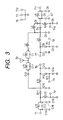
- Fig. 3 is a circuit diagram showing an example of circuit configuration of the front-end module 1.
- signs T1 through T12 are external connection electrodes.
- the external connection electrode T9 is an external connection electrode to the antenna.
- Coils L1, L2, L11 and capacitors C1, C11, C12 constitute a band splitter circuit.
- the circuit from the coil L1 and the capacitor C1 to the external connection electrode T11 (circuit on the right in the figure) is a circuit supporting the DCS system (1.8 GHz band).
- the circuit from the coil L11 and the capacitor C11 to the external connection electrode T1 (circuit on the left in the figure) is a circuit supporting the GSM system (900 MHz band).
- T11 is an external connection electrode connected to a transmitter circuit of the DCS system.
- T7 is an external connection electrode connected to a receiver circuit of the DCS system.
- T8 is an external connection electrode grounded by an external circuit.
- T10 is an external connection electrode for applying a control signal to switch between transmission and reception for the DCS system.
- a coil L6 and capacitors C6 through C8 constitute a low-pass filter.
- Diodes D1, D2, coils L3 through L5, and capacitors C2 through C5 and C9 constitute a transmission/reception selector switch.
- T1 is an external connection electrode connected to a transmitter circuit of the GSM system.
- T5 is an external connection electrode connected to a receiver circuit of the GSM system.
- T2 is an external connection electrode for applying a control signal to switch between transmission and reception for the GSM system.
- T4 is an external connection electrode grounded by an external circuit.
- a coil L14 and capacitors C17 through C19 constitute a low-pass filter.
- Diodes D11, D12, coils L12, L13, capacitors C13 through C16 constitute a transmission/reception selector switch.
- T3, T6, T12 are external connection electrodes connected to ground electrodes inside the front-end module.
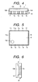
- Figs. 4 through 6 are external views of the front-end module 1.
- Fig. 4 is a front view in the same direction as Fig. 1.
- Fig. 5 is a plane view and
- Fig. 6 is a side view in the direction orthogonal to the direction of Fig. 4.
- the right and left ends (top of the figure) of the shield case 15 are bent downward to lie at right angles to the plane section. Ends 15A, 15B that are bent are respectively fixed to external connection electrodes T6, T12 as ground electrodes.
- said surface-mounted components 11, 12 are not shown.
- 15C is a hole made in the shield case 15 that shows the direction of the front-end module 1.
- external connection electrodes T1 through T12 for connecting circuits of said front-end module are arranged on the periphery of the front-end module. These external connection electrodes T1 through T12 are used to mount to connect the front-end module on a circuit substrate of a mobile telephone set.
- the front-end module in this example has a height of 1.8 mm including the shield case, a horizontal width of 6.5 mm in Fig. 5, and a vertical width of 4.8 mm.
- a ground electrode pattern 201 is formed on almost the entire surface of the dielectric layer 35 in the lower section.
- a facing electrode pattern 202 of the ground capacitor is formed on the dielectric layer 34 adjacent to the dielectric layer 35. While a plurality of facing electrode patterns are formed as well as said facing electrode pattern 202, signs are omitted for clarity.
- a ground pattern 203 and other electrode patterns whose signs are omitted are formed on the dielectric layer 33 adjacent to the dielectric layer 34.
- dielectric layers 28 through 32 where few patterns are formed.
- a via hole 204 for connecting patterns on vertically adjacent dielectric layers
- a connection pattern 205 for connecting via holes
- an electrode pattern 206 other electrode patterns whose signs are omitted, and some of the capacitor electrode patterns for the band splitter circuit.
- dielectric layers 22 through 27 are laminated above.
- coils and capacitors made by using coil conductor patterns and capacitor electrode patterns.
- Electrode patterns 211 through 218 are capacitor electrode patterns for the band splitter circuit.
- the capacitor electrode patterns for the band splitter circuit 211 through 218 are formed to be located at the center in vertical direction in the figure, that is, at the center of the plane, in each of the dielectric layers 22 through 29 in Fig. 2.
- On each of the dielectric layers 22 through 26 are formed circuits supporting the DCS system in the upper section and circuits supporting the GSM system in the lower section in the figure.
- connection pattern 221 for the DCS system in the upper section in the figure On the dielectric layer 27 is formed a connection pattern 221 for the DCS system in the upper section in the figure. On the dielectric layers 22 through 26 are formed coil conductor patterns 222 through 226 for the DCS system in the upper section in the figure.
- connection pattern 231 for the GSM system in the lower section in the figure On the dielectric layer 27 is formed a connection pattern 231 for the GSM system in the lower section in the figure. On the dielectric layers 22 through 26 are formed coil conductor patterns 232 through 236 for the GSM system in the lower section in the figure.
- connection pattern 219 On the dielectric layer 21 is formed a connection pattern 219.
- the surface-mounted components 11, 12 are diodes, chip resistors, chip capacitors or chip inductors and arranged as required according to the circuit configuration.
- connection pattern 219 is connected to a corresponding via hole according to the circuit configuration.
- external connection electrodes T1 through T12 for example external connection electrodes T8, T4 are connected to connection patterns 221, 231 as internal electrode drawing patterns.
- arrangement of the dielectric layers 21 through 36 shown in Figs. 1 and 2 is determined considering the electrical characteristics and the reduction ratio that accompanies firing of green sheets.
- the uppermost dielectric layer 21 has a dielectric constant of about 11 and a green sheet with a smaller reduction ratio is selected.
- Dielectric layers 22 through 32 below the dielectric layer 21 have a dielectric constant of about 7.3 and green sheets with a slightly larger reduction ratio are selected.
- Dielectric layers 33, 34 below the dielectric layers 22 through 32 have a dielectric constant of about 11, same as the uppermost dielectric layer 21, and green sheets with a smaller reduction ratio are selected.
- Dielectric layers 35, 36 below the dielectric layers 33, 34 have a dielectric constant of about 7.3, same as the dielectric layers 22 through 32, and green sheets with a slightly larger reduction ratio are selected.
- the dielectric layers 22 through 26 mainly form coil conductor patterns and the dielectric layers 27 through 32 mainly form connection patterns.
- a material having a dielectric constant of about 7.3 is selected for each of the dielectric layers 22 through 32.
- the dielectric layers 33, 34 are dielectric layers between electrodes constituting capacitors and a material having a dielectric constant of about 11 is selected for each of them. It is thus easy to obtain capacity as a capacitor.
- the dielectric layers 33, 34 have a small reduction ratio that accompanies firing and the dielectric layers 22 through 32 have a larger reduction ratio, thus causing deformation during firing. It is possible to prevent deformation during firing by selecting a material with small reduction ratio, same as the dielectric layers 33, 34, for the uppermost dielectric layer 21.
- the antenna switch is composed of a diode and an LC circuit, with the LC circuit formed in a multilayer substrate. This eliminates the need for considering the impedance matching of the strip lines, unlike a conventional configuration via diodes, capacitors and ⁇ /4 strip lines generally used in high-frequency circuits. It is not necessary to provide a dielectric layer for matching the impedance, thus providing a more low-thickness multilayer substrate.
Landscapes
- Engineering & Computer Science (AREA)
- Computer Networks & Wireless Communication (AREA)
- Signal Processing (AREA)
- Transceivers (AREA)
- Filters And Equalizers (AREA)
- Production Of Multi-Layered Print Wiring Board (AREA)
- Coils Or Transformers For Communication (AREA)
Abstract
Description
Claims (4)
- A front-end module used for a plurality of different communications systems, comprising:a band splitter circuit connected to an antenna;at least an antenna switch connected to the antenna via the band splitter circuit to switch the antenna to transmitter circuits and receiver circuits of different communications systems; andat least a filter for removing high frequencies;wherein the front end circuit constitute an integrated module with components mounted on a multilayer substrate, andsaid multilayer substrate arranges a pattern of said band splitter circuit at the center in the plane direction, anda plurality of antenna switch conductor patterns using different communications systems are symmetrically arranged with respect to the pattern for the band splitter circuit.
- A front-end module according to claim 1, wherein said multilayer substrate is composed of a plurality of laminated dielectric layers, andthe dielectric layers constituting said multilayer substrate are split into a plurality of dielectric layers laminated adjacently where coil conductor patterns are mainly formed, and a plurality of dielectric layers laminated adjacently where capacitor electrode patterns are mainly formed, andsaid dielectric layers where coil conductor patterns are mainly formed select a material that shows a dielectric constant lower than that of said dielectric layers where capacitor electrode patterns are mainly formed.
- A front-end module according to claim 2, wherein the dielectric layers laminated adjacently where capacitor electrode patterns are mainly formed are provided beneath the dielectric layers laminated adjacently where coil conductor patterns are mainly formed,layers comprising a similar material to that of the dielectric layers where capacitor electrode patterns are mainly formed are provided on top of said dielectric layers where coil conductor patterns are mainly formed, in order to prevent deformation caused by the difference in the reduction ratio that accompanies firing.
- A front end module according to any of claims 1 through 3, wherein said antenna switch is composed of at least a diode and at least an LC circuit, and said filter and said band splitter circuit are composed of LC circuits,said LC circuits are formed in said multilayer substrate, andpart of said LC circuits is connected to a diode arranged on the upper face of said multilayer substrate through a via hole.
Applications Claiming Priority (2)
| Application Number | Priority Date | Filing Date | Title |
|---|---|---|---|
| JP2000250393A JP3750792B2 (en) | 1999-10-04 | 2000-08-21 | Front-end module for mobile communication equipment |
| JP2000250393 | 2000-08-21 |
Publications (2)
| Publication Number | Publication Date |
|---|---|
| EP1182790A2 true EP1182790A2 (en) | 2002-02-27 |
| EP1182790A3 EP1182790A3 (en) | 2006-03-08 |
Family
ID=18739969
Family Applications (1)
| Application Number | Title | Priority Date | Filing Date |
|---|---|---|---|
| EP01108422A Withdrawn EP1182790A3 (en) | 2000-08-21 | 2001-04-03 | Front end module for mobile communications apparatus |
Country Status (6)
| Country | Link |
|---|---|
| US (1) | US6600385B2 (en) |
| EP (1) | EP1182790A3 (en) |
| KR (1) | KR100611421B1 (en) |
| CN (1) | CN1180560C (en) |
| AR (1) | AR034549A1 (en) |
| BR (1) | BR0101369A (en) |
Families Citing this family (10)
| Publication number | Priority date | Publication date | Assignee | Title |
|---|---|---|---|---|
| US6865376B2 (en) * | 2001-07-03 | 2005-03-08 | Kyocera Wireless Corp. | System and method for a GPS enabled antenna |
| US7383058B2 (en) * | 2002-07-16 | 2008-06-03 | Intel Corporation | RF/microwave system with a system on a chip package or the like |
| US6816032B1 (en) * | 2002-09-03 | 2004-11-09 | Amkor Technology, Inc. | Laminated low-profile dual filter module for telecommunications devices and method therefor |
| US7376440B2 (en) * | 2003-04-16 | 2008-05-20 | Kyocera Wireless Corp. | N-plexer systems and methods for use in a wireless communications device |
| US7167688B2 (en) * | 2003-07-30 | 2007-01-23 | Chi Mei Communication Systems, Inc. | RF transceiver module formed in multi-layered ceramic |
| KR100890711B1 (en) * | 2005-04-28 | 2009-03-27 | 가부시키가이샤 무라타 세이사쿠쇼 | High frequency switching module and method for adjusting frequency characteristic of high frequency circuit |
| KR100747978B1 (en) * | 2005-06-17 | 2007-08-08 | 엘지이노텍 주식회사 | Front end module and fabricating method thereof |
| CN100356629C (en) * | 2005-07-01 | 2007-12-19 | 清华大学 | Mobile-terminal multi-antenna system |
| JP4441886B2 (en) * | 2006-03-31 | 2010-03-31 | Tdk株式会社 | High frequency module |
| US9705558B2 (en) * | 2011-02-08 | 2017-07-11 | Qorvo Us, Inc. | Harmonic rejected antenna switch |
Family Cites Families (16)
| Publication number | Priority date | Publication date | Assignee | Title |
|---|---|---|---|---|
| WO1993019527A1 (en) * | 1992-03-19 | 1993-09-30 | Tdk Corporation | Hybrid coupler |
| JPH05335183A (en) * | 1992-05-28 | 1993-12-17 | Murata Mfg Co Ltd | Electronic component provided with multilayer board and manufacture thereof |
| JPH06232005A (en) * | 1993-02-01 | 1994-08-19 | Tdk Corp | Lc composite component |
| JP3031178B2 (en) | 1994-09-28 | 2000-04-10 | 株式会社村田製作所 | Composite high frequency components |
| JPH09261110A (en) | 1996-03-21 | 1997-10-03 | Tdk Corp | Antenna switch |
| US5999065A (en) | 1995-08-24 | 1999-12-07 | Murata Manufacturing Co., Ltd. | Composite high-frequency component |
| JPH11112264A (en) * | 1997-10-08 | 1999-04-23 | Murata Mfg Co Ltd | Filter |
| JP2983016B2 (en) | 1997-12-03 | 1999-11-29 | 日立金属株式会社 | High frequency switch module for multi-band |
| JPH11168303A (en) * | 1997-12-05 | 1999-06-22 | Hitachi Metals Ltd | High frequency switch module |
| JP3322199B2 (en) * | 1998-01-06 | 2002-09-09 | 株式会社村田製作所 | Multilayer ceramic substrate and method of manufacturing the same |
| EP1650865B1 (en) | 1998-10-27 | 2009-10-21 | Murata Manufacturing Co., Ltd. | Composite high frequency component and mobile communication device including the same |
| JP3304900B2 (en) | 1998-11-25 | 2002-07-22 | 株式会社村田製作所 | Composite high frequency component and mobile communication device using the same |
| JP3304931B2 (en) | 1998-10-27 | 2002-07-22 | 株式会社村田製作所 | Composite high frequency component and mobile communication device using the same |
| JP3304901B2 (en) | 1998-11-27 | 2002-07-22 | 株式会社村田製作所 | Composite high frequency component and mobile communication device using the same |
| JP3304898B2 (en) | 1998-11-20 | 2002-07-22 | 株式会社村田製作所 | Composite high frequency component and mobile communication device using the same |
| JP3304902B2 (en) | 1998-12-14 | 2002-07-22 | 株式会社村田製作所 | Composite high frequency component and mobile communication device using the same |
-
2001
- 2001-03-07 KR KR1020010011594A patent/KR100611421B1/en not_active Expired - Fee Related
- 2001-03-07 US US09/799,569 patent/US6600385B2/en not_active Expired - Fee Related
- 2001-04-02 BR BR0101369-6A patent/BR0101369A/en not_active Application Discontinuation
- 2001-04-03 EP EP01108422A patent/EP1182790A3/en not_active Withdrawn
- 2001-04-03 AR ARP010101572A patent/AR034549A1/en unknown
- 2001-04-03 CN CNB011165693A patent/CN1180560C/en not_active Expired - Fee Related
Also Published As
| Publication number | Publication date |
|---|---|
| BR0101369A (en) | 2004-05-25 |
| CN1339886A (en) | 2002-03-13 |
| CN1180560C (en) | 2004-12-15 |
| US6600385B2 (en) | 2003-07-29 |
| US20020021182A1 (en) | 2002-02-21 |
| AR034549A1 (en) | 2004-03-03 |
| KR20020015260A (en) | 2002-02-27 |
| EP1182790A3 (en) | 2006-03-08 |
| KR100611421B1 (en) | 2006-08-09 |
Similar Documents
| Publication | Publication Date | Title |
|---|---|---|
| US6822534B2 (en) | Laminated electronic component, laminated duplexer and communication device | |
| EP0921642B1 (en) | Multiband high-frequency switching module | |
| EP1291956B1 (en) | Frequency separator for use in dual-band mobile phone terminals | |
| JP3903456B2 (en) | High frequency switch module for multiband | |
| US20090121806A1 (en) | Noise filter array | |
| US6600385B2 (en) | Front end module for mobile communications apparatus | |
| US6856213B2 (en) | High frequency composite switch module | |
| US20230208377A1 (en) | Filter, multiplexer, and communication module | |
| JP4120902B2 (en) | Multi-band high-frequency switch module | |
| JP3750792B2 (en) | Front-end module for mobile communication equipment | |
| JPH03272213A (en) | High frequency branching filter | |
| JP4111344B2 (en) | Front-end module for mobile communication equipment | |
| JP4130442B2 (en) | Front-end module for mobile communication equipment | |
| JP3750796B2 (en) | Module for mobile communication equipment | |
| JP4678570B2 (en) | Demultiplexer and high frequency composite parts using the same | |
| JP2005192241A (en) | Front-end module for mobile communications equipment | |
| KR100430824B1 (en) | Antenna switch module including coupler and fabrication method thereof | |
| JP2001119258A (en) | Branching filter | |
| JP2002300081A (en) | High frequency module | |
| JP2002280926A (en) | High-frequency switch module for multiband | |
| KR100784411B1 (en) | Front End Modules for Dual Band Terminals | |
| JP3824229B2 (en) | High frequency switch module for multiband | |
| JP2003151856A (en) | Laminated electronic component and method of manufacturing the same | |
| KR100616640B1 (en) | Integrated Dual Band Lowpass Filter | |
| JP2005341319A (en) | High frequency module and wireless communication device |
Legal Events
| Date | Code | Title | Description |
|---|---|---|---|
| PUAI | Public reference made under article 153(3) epc to a published international application that has entered the european phase |
Free format text: ORIGINAL CODE: 0009012 |
|
| AK | Designated contracting states |
Kind code of ref document: A2 Designated state(s): AT BE CH CY DE DK ES FI FR GB GR IE IT LI LU MC NL PT SE TR |
|
| AX | Request for extension of the european patent |
Free format text: AL;LT;LV;MK;RO;SI |
|
| PUAL | Search report despatched |
Free format text: ORIGINAL CODE: 0009013 |
|
| AK | Designated contracting states |
Kind code of ref document: A3 Designated state(s): AT BE CH CY DE DK ES FI FR GB GR IE IT LI LU MC NL PT SE TR |
|
| AX | Request for extension of the european patent |
Extension state: AL LT LV MK RO SI |
|
| 17P | Request for examination filed |
Effective date: 20060405 |
|
| AKX | Designation fees paid |
Designated state(s): DE FR GB |
|
| 17Q | First examination report despatched |
Effective date: 20070917 |
|
| RAP1 | Party data changed (applicant data changed or rights of an application transferred) |
Owner name: TDK CORPORATION |
|
| RAP1 | Party data changed (applicant data changed or rights of an application transferred) |
Owner name: TDK CORPORATION |
|
| GRAP | Despatch of communication of intention to grant a patent |
Free format text: ORIGINAL CODE: EPIDOSNIGR1 |
|
| INTG | Intention to grant announced |
Effective date: 20180403 |
|
| RAP1 | Party data changed (applicant data changed or rights of an application transferred) |
Owner name: SNAPTRACK, INC. |
|
| STAA | Information on the status of an ep patent application or granted ep patent |
Free format text: STATUS: THE APPLICATION IS DEEMED TO BE WITHDRAWN |
|
| 18D | Application deemed to be withdrawn |
Effective date: 20180814 |
|
| RIC1 | Information provided on ipc code assigned before grant |
Ipc: H04B 1/18 20060101AFI20011214BHEP |