JP4678570B2 - Demultiplexer and high frequency composite parts using the same - Google Patents
Demultiplexer and high frequency composite parts using the same Download PDFInfo
- Publication number
- JP4678570B2 JP4678570B2 JP2004138664A JP2004138664A JP4678570B2 JP 4678570 B2 JP4678570 B2 JP 4678570B2 JP 2004138664 A JP2004138664 A JP 2004138664A JP 2004138664 A JP2004138664 A JP 2004138664A JP 4678570 B2 JP4678570 B2 JP 4678570B2
- Authority
- JP
- Japan
- Prior art keywords
- port
- frequency band
- capacitance
- circuit
- filter
- Prior art date
- Legal status (The legal status is an assumption and is not a legal conclusion. Google has not performed a legal analysis and makes no representation as to the accuracy of the status listed.)
- Expired - Fee Related
Links
Images


Description
本発明は、携帯電話などの移動体通信機器に用いられる分波器に関し、具体的には高周波回路(フロントエンド部)に用いられ、周波数の異なる少なくとも2つの通信システムの高周波信号を分波する分波器と、これを用いた高周波複合部品に関する。 The present invention relates to a duplexer used in a mobile communication device such as a cellular phone. Specifically, the duplexer is used in a high frequency circuit (front end unit) and demultiplexes high frequency signals of at least two communication systems having different frequencies. The present invention relates to a duplexer and a high-frequency composite component using the duplexer.
近年移動体通信機器のひとつの形態として、携帯電話一台で2つ以上の通信システムで通話を可能とするマルチバンド携帯電話がある。この携帯電話にあっては、それぞれのシステムに対応する周波数の高周波信号を分波する分波回路が必要である。
この様な分波回路として、複数のフィルタ回路を組み合わせて構成される分波器がある。特許文献1には、フィルタ回路をインダクタンス素子、キャパシタンス素子で構成し、各素子を積層体内に電極パターンで形成した積層構造の積層型分波器が提案されている。図6に、その等価回路図を示す。
この積層型分波器は、誘電体からなる絶縁層を積層一体化した積層体の内部にパターン電極を形成し、このパターン電極により構成したインダクタンス素子とキャパシタンス素子とを直列接続して2つのノッチ回路(直列共振回路)を構成し、第1ポートP1と第2ポートP2との間に、ローパスフィルタ回路(他のインダクタンス素子)と第1直列共振回路を配置し、第1ポートP1と第3ポートP3との間に、ハイパスフィルタ回路(他のキャパシタンス素子)と第2直列共振回路を配置して構成される。
前記第2直列共振回路は、周波数f1で挿入損失が最大となるように構成され、前記第1直列共振回路は前記周波数f1と異なる周波数f2で挿入損失が最大となるように構成されている。このため、第1ポートP1に入力された周波数f1のマイクロ波信号は、第3ポートP3に出力されず、また第1ポートP1に入力された周波数f2のマイクロ波信号は、第2ポートP2に出力されないため、マイクロ波信号の分配を行うことが出来る。
As such a demultiplexing circuit, there is a demultiplexer configured by combining a plurality of filter circuits.
In this laminated duplexer, a patterned electrode is formed inside a laminated body in which insulating layers made of a dielectric are laminated and integrated, and an inductance element and a capacitance element constituted by the patterned electrode are connected in series to form two notches. Circuit (series resonant circuit), a low-pass filter circuit (another inductance element) and a first series resonant circuit are arranged between the first port P1 and the second port P2, and the first port P1 and the third A high-pass filter circuit (another capacitance element) and a second series resonance circuit are arranged between the port P3.
The second series resonance circuit is configured to maximize the insertion loss at the frequency f1, and the first series resonance circuit is configured to maximize the insertion loss at a frequency f2 different from the frequency f1. Therefore, the microwave signal having the frequency f1 input to the first port P1 is not output to the third port P3, and the microwave signal having the frequency f2 input to the first port P1 is not input to the second port P2. Since it is not output, the microwave signal can be distributed.
現在、移動体通信装置として複数の周波数帯の通信システム、例えばDCS1800(送信周波数1710〜1785MHz、受信周波数1805〜1880MHz)とGSM900(送信周波数880〜915MHz、受信周波数925〜960MHz)とで動作が可能なデュアルバンド携帯電話、DCS1800及びPCS1900(送信周波数1850〜1910MHz、受信周波数1930〜1990MHz)とGSM900とで動作が可能なトリプルバンド携帯電話や、前記トリプルバンド携帯電話にGSM850(送信周波数824〜849MHz、受信周波数869〜894MHz)のシステムを加えたクワッドバンド携帯電話が提案されており、これを総称してマルチバンド携帯電話と呼称している。
これら通信システムの利用周波数帯を大別すると、周波数帯域800MHz〜1GHzを利用する通信システムと、相対的に高周波数帯域の1.5GHz〜2.4GHzを利用する通信システムとになる。
Currently, it can operate as a mobile communication device in communication systems of multiple frequency bands such as DCS1800 (transmission frequency 1710 to 1785 MHz, reception frequency 1805 to 1880 MHz) and GSM900 (transmission frequency 880 to 915 MHz, reception frequency 925 to 960 MHz). Dual-band mobile phone, DCS1800 and PCS1900 (transmission frequency 1850-1910 MHz, reception frequency 1930-1990 MHz) and triple-band mobile phone that can operate with GSM900, and GSM850 (transmission frequency 824-849 MHz, A quad-band mobile phone to which a system having a reception frequency of 869 to 894 MHz) has been proposed, and this is collectively called a multi-band mobile phone.
The use frequency bands of these communication systems are roughly classified into a communication system using a frequency band of 800 MHz to 1 GHz and a communication system using a relatively high frequency band of 1.5 GHz to 2.4 GHz.
近年の携帯電話のマルチバンド化に伴い、前記分波回路では複数の低周波数帯域の通信システムと複数の高周波数帯域の通信システムとを分波することが必要と成ってきた。しかしながら従来の分波回路では、複数の通信システムの周波数帯域を包含する広周波数帯域にわたって減衰量を確保することが困難であって、このため、通過帯域において所望の挿入損失を得られないといった問題があった。
そこで本発明では、2つ以上の通信システムで通話を可能とするマルチバンド携帯電話に用いられ、前記通信システムに対応する高周波信号を分波する分波器において、広帯域にわたって減衰量を得ることでき、通過帯域において優れた挿入損失特性が得られる小型の分波器と、これを用いた高周波複合部品を提供することを目的とする。
With the recent increase in the number of multi-band cellular phones, it has become necessary for the demultiplexing circuit to demultiplex a plurality of low frequency band communication systems and a plurality of high frequency band communication systems. However, in the conventional branching circuit, it is difficult to secure an attenuation amount over a wide frequency band including the frequency bands of a plurality of communication systems. For this reason, a desired insertion loss cannot be obtained in the pass band. was there.
Therefore, in the present invention, an attenuation amount can be obtained over a wide band in a duplexer that is used in a multiband mobile phone that enables a call in two or more communication systems and demultiplexes a high-frequency signal corresponding to the communication system. An object of the present invention is to provide a small duplexer that can provide excellent insertion loss characteristics in the passband, and a high-frequency composite component using the same.
本発明は、周波数の異なる少なくとも2つの通信システムの高周波信号を分波する分波器であって、第1ポートと第2ポートとの間に接続され、第1の周波数帯域を通過周波数帯域とする第1フィルタと、第1ポートと第3ポートとの間に接続され、第2の周波数帯域を通過周波数帯域とする第2フィルタとを備え、前記第1フィルタは、第1ポートと第2ポートとの間に接続された第1インダクタンス素子と、前記第1インダクタンス素子と並列接続し並列共振回路を形成する第1キャパシタンス素子と、前記第1インダクタンス素子の第2ポート側とグランドとの間に配置され、第2インダクタンス素子及び第2キャパシタンス素子を備えた第1直列共振回路を備え、前記第2フィルタは、第1ポートと第3ポートとの間に接続された第3キャパシタンス素子と、前記第3キャパシタンス素子と直列接続される第4キャパシタンス素子と、前記第3キャパシタンス素子と第4キャパシタンス素子との接続点とグランドとの間に配置され、第3インダクタンス素子及び第5キャパシタンス素子を備えた第2直列共振回路を有し、 前記第1から第3インダクタンス素子と、第2から第5キャパシタンス素子とは、積層体に形成された電極パターンにより構成され、前記第1キャパシタンス素子は、異なる誘電体層に形成された前記第1インダクタンス素子を構成する電極パターン間を、他の電極パターンとの間よりも積層方向に近接させて生じた浮遊容量のみで形成され、前記第3及び前記第4キャパシタンス素子の電極パターンが前記第1インダクタンス素子を構成する電極パターンと積層方向に重なり、誘電体層を介して隣り合う前記第1インダクタンス素子の電極パターンと前記第3キャパシタンス素子の電極パターンとを、少なくとも75μmの間隔をもって配置した分波器である。 The present invention is a duplexer that demultiplexes a high-frequency signal of at least two communication systems having different frequencies, and is connected between a first port and a second port, and the first frequency band is defined as a passing frequency band. And a second filter connected between the first port and the third port and having a second frequency band as a pass frequency band, wherein the first filter includes a first port and a second filter. A first inductance element connected between the first inductance element, a first capacitance element connected in parallel with the first inductance element to form a parallel resonance circuit, and a second port side of the first inductance element and a ground And a first series resonant circuit having a second inductance element and a second capacitance element, wherein the second filter is connected between the first port and the third port. A capacitance element; a fourth capacitance element connected in series with the third capacitance element; and a connection point between the third capacitance element and the fourth capacitance element and a ground, and a third inductance element and a fifth capacitance element. A second series resonant circuit including a capacitance element, wherein the first to third inductance elements and the second to fifth capacitance elements are configured by electrode patterns formed in a laminate, and the first capacitance The element is formed of only stray capacitance generated between the electrode patterns constituting the first inductance element formed in different dielectric layers closer to each other in the stacking direction than between the other electrode patterns . 3 and the electrode pattern of the fourth capacitance element constitutes the first inductance element. Ting overlap in the stacking direction, and the electrode pattern of the first inductance element adjacent with the dielectric layer and the electrode pattern of the third capacitance element, a duplexer arranged at an interval of at least 75 [mu] m.
本発明においては、前記第1直列共振回路は、第2の周波数帯域内に減衰極を有し、
前記並列共振回路は、第1の周波数帯域の2.5〜3倍の周波数帯域内に減衰極を有し、
前記第2直列共振回路は、第1の周波数帯域内に減衰極を有するように構成するのが好ましい。
In the present invention , the first series resonant circuit has an attenuation pole in the second frequency band,
It said parallel resonant circuit, an attenuation pole possess a 2.5-3 times in the frequency band of the first frequency band,
The second series resonant circuit is preferably configured to have an attenuation pole in the first frequency band .
本発明においては、更に前記第2ポートにフィルタ回路或いはスイッチ回路を接続し、及び/又は前記第3ポートに他のフィルタ回路或いは他のスイッチ回路を接続し、前記フィルタ回路、スイッチ回路を前記積層体に分波器とともに構成して高周波複合部品とするのも好ましい。 In the present invention, a filter circuit or a switch circuit is further connected to the second port, and / or another filter circuit or another switch circuit is connected to the third port, and the filter circuit and the switch circuit are connected to the stacked layer. It is also preferable that the body is configured with a duplexer to form a high frequency composite part.
本発明の分波器は、小型でありながら広帯域にわたって減衰量を得ることでき、通過帯域において優れた挿入損失特性が得られるため、2つ以上の通信システム、特には3つ以上の通信システムで通話を可能とするマルチバンド携帯電話に有用である。 Since the duplexer of the present invention is small in size and can obtain attenuation over a wide band, and an excellent insertion loss characteristic can be obtained in the pass band, it can be used in two or more communication systems, particularly three or more communication systems. This is useful for a multi-band mobile phone that enables calls.
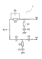
図1は、本発明の一実施例に係る分波器の等価回路を示す図である。この分波器は、第1ポートP1と第2ポートP2との間に接続され、第1の周波数帯域f1を通過周波数帯域とする第1フィルタと、第1ポートP1と第3ポートP3との間に接続され、第2の周波数帯域f2を通過周波数帯域とする第2フィルタとを備えている。第1の周波数帯域f1は、第2の周波数帯域f2と比較し低周波数側に有り、互いに重なり合わない周波数帯に設定される。前記第1フィルタは、第2の周波数帯域(高周波数帯域)f2で大きな減衰量を示すものであり、前記第2フィルタは、第1の周波数帯域(低周波数帯域)f1で大きな減衰量を示す。 FIG. 1 is a diagram showing an equivalent circuit of a duplexer according to an embodiment of the present invention. The duplexer is connected between the first port P1 and the second port P2, and includes a first filter having a first frequency band f1 as a pass frequency band, and a first port P1 and a third port P3. And a second filter connected in between and having the second frequency band f2 as a pass frequency band. The first frequency band f1 is on the lower frequency side compared to the second frequency band f2, and is set to a frequency band that does not overlap each other. The first filter exhibits a large attenuation in the second frequency band (high frequency band) f2, and the second filter exhibits a large attenuation in the first frequency band (low frequency band) f1. .
第1ポートP1と第2ポートP2との間に接続された第1フィルタは、一端が第1ポートP1に接続する第1インダクタンス素子L1と、前記第1インダクタンス素子と並列接続し並列共振回路を形成する第1キャパシタンス素子と、前記第1インダクタンス素子の第2ポート側とグランドとの間に配置され、第2インダクタンス素子及び第2キャパシタンス素子を備えた第1直列共振回路を備え、前記第1直列共振回路は、第2の周波数帯域f2内に減衰極を有し、挿入損失が最大となるように構成されている。前記並列共振回路は、第1の周波数帯域の2.5〜3倍の周波数帯域内に減衰極を有するように構成されている。このように構成することで、広帯域にわたって大きな減衰量を得ている。 The first filter connected between the first port P1 and the second port P2 has a first inductance element L1 having one end connected to the first port P1, and a parallel resonance circuit connected in parallel with the first inductance element. A first capacitance element to be formed; and a first series resonance circuit that is disposed between the second port side of the first inductance element and the ground, and includes a second inductance element and a second capacitance element. The series resonant circuit has an attenuation pole in the second frequency band f2 and is configured to maximize the insertion loss. The parallel resonant circuit is configured to have an attenuation pole in a frequency band 2.5 to 3 times the first frequency band. With this configuration, a large attenuation is obtained over a wide band.
第1ポートP1と第3ポートP3との間に接続された第2フィルタは、第1ポートP1と第3ポートP3との間に接続された第3キャパシタンス素子C3と、前記第3キャパシタンス素子C3と直列接続される第4キャパシタンス素子C4と、前記第3キャパシタンス素子C3と第4キャパシタンス素子C4との接続点とグランドとの間に配置され、第3インダクタンス素子L3及び第5キャパシタンス素子C5を備えた第2直列共振回路を有し、前記第2直列共振回路は、第1の周波数帯域f1内に減衰極を有し、挿入損失が最大となるように構成されている。また従来の分波器と比べて、第4キャパシタンス素子C4を更に追加することで、低周波数帯域で広帯域にわたって大きな減衰量を得ている。 The second filter connected between the first port P1 and the third port P3 includes a third capacitance element C3 connected between the first port P1 and the third port P3, and the third capacitance element C3. A fourth capacitance element C4 connected in series, and a connection point between the third capacitance element C3 and the fourth capacitance element C4 and the ground, and a third inductance element L3 and a fifth capacitance element C5. The second series resonant circuit has an attenuation pole in the first frequency band f1, and is configured to maximize the insertion loss. Compared to the conventional duplexer, the fourth capacitance element C4 is further added to obtain a large attenuation over a wide band in the low frequency band.
このように構成することで、第1ポートP1に入力した第1の周波数帯域f1は、第2ポートP2に表れるが、第3ポートP3には出力されず、また、第1ポートP1に入力した第2の周波数帯域f1は、第3ポートP3に表れるが、第2ポートP2には出力されないため、高周波信号を低損失で分波することが出来る。 With this configuration, the first frequency band f1 input to the first port P1 appears at the second port P2, but is not output to the third port P3, and is input to the first port P1. Although the second frequency band f1 appears at the third port P3 but is not output to the second port P2, the high frequency signal can be demultiplexed with low loss.
本発明の分波器では、前記第1乃至第5インダクタンス素子と、第1乃至第第6キャパシタンス素子とを、積層体に形成された電極パターンにより構成し、前記第1キャパシタンス素子は、前記第1インダクタンス素子を構成する電極パターンを、誘電体層を介して積層方向に略対向させて形成される浮遊容量で構成している。このため、第1キャパシタンス素子を形成する電極パターンを、更に追加する必要が無いので、分波器が大型化することがない。 In the duplexer of the present invention, the first to fifth inductance elements and the first to sixth capacitance elements are configured by electrode patterns formed in a laminate, and the first capacitance element is the first capacitance element. An electrode pattern constituting one inductance element is constituted by a stray capacitance formed so as to be substantially opposed to each other in the stacking direction via a dielectric layer. For this reason, since it is not necessary to add the electrode pattern which forms a 1st capacitance element further, a splitter is not enlarged.
本発明を以下の実施例によりさらに詳細に説明するが、本発明はそれらに限定されるものではない。
図2は本発明の分波器を含む、マルチバンド携帯電話のフロントエンド部の等価回路である。ここでは、分波器1に加えて、フィルタ回路LPF1、LPF2、スイッチ回路SW1,SW2を配置した第1乃至3の通信システムに対応したにフロントエンド部ついて説明する。なお説明においては、第1の通信システムをGSM900(送信周波数880〜915MHz、受信周波数925〜960MHz)、第2の通信システムをDCS1800(送信周波数1710〜1785MHz、受信周波数1805〜1880MHz)、第3の通信システムをPCS1900(送信周波数1850〜1910MHz、受信周波数1930〜1990MHz)としている。
The present invention will be described in more detail with reference to the following examples, but the present invention is not limited thereto.
FIG. 2 is an equivalent circuit of a front end portion of a multiband mobile phone including the duplexer of the present invention. Here, the front end unit corresponding to the first to third communication systems in which the filter circuits LPF1 and LPF2 and the switch circuits SW1 and SW2 are arranged in addition to the
図2に示したマルチバンド携帯電話器のフロントエンド部では、分波器1の第1ポートP1をアンテナANTと接続し、分波回路1の第2ポートP2、第3ポートP3には、スイッチ回路SW1,SW2が接続される。スイッチ回路SW1,SW2には、フィルタ回路LPF1、LPF2を介して送信回路EGSMTX、DCS/PCSTXが接続され、また受信回路EGSMRX,DCSRX、PCSRXが接続される。
前記分波器1は、GSM900或いはDCS1800,PCS1900の送受信信号が、互いの信号経路に回りこまないように、ローパスフィルタ、バンドパスフィルタ、ノッチフィルタから選ばれる複数のフィルタ回路で構成されるが、本実施例においては、図1で示した分波器を用いている。図中、点線で示した部分が浮遊容量で形成した第1キャパシタンス素子である。
2, the first port P1 of the
The
既に分波器の構成については説明しているので省略するが、前記第1直列共振回路により、第2の周波数帯域内(1710MHz〜1990MHz)に減衰極を形成し、前記並列共振回路により、第1の周波数帯域(880MHz〜960MHz)の2.5〜3倍の周波数帯域内(2200MHz〜2880MHz)に減衰極を形成し、前記第1直列共振回路の共振周波数を前記並列共振回路の共振周波数よりも低周波数に設定している。そして、前記第2直列共振回路は、第1の周波数帯域内(880MHz〜960MHz)に減衰極を有するように構成している。
このように構成することで、本発明の分波器は、広帯域にわたって大きな減衰量を得ることが出来、通過帯域において優れた挿入損失特性が得られるため、第1ポートP1に入力した第1の周波数帯域f1は、第2ポートP2に表れるが、第3ポートP3には出力されず、また、第1ポートP1に入力した第2の周波数帯域f1は、第3ポートP3に表れるが、第2ポートP2には出力されないため、高周波信号を分波することが出来る。分波された高周波信号は、分波回路の後段に配置されたスイッチ回路SW1,SW2へと入力する。
Although the configuration of the duplexer has already been described, a description thereof will be omitted. However, an attenuation pole is formed in the second frequency band (1710 MHz to 1990 MHz) by the first series resonance circuit, and An attenuation pole is formed in a frequency band (2200 MHz to 2880 MHz) 2.5 to 3 times the frequency band of 1 (880 MHz to 960 MHz), and the resonance frequency of the first series resonance circuit is determined from the resonance frequency of the parallel resonance circuit. Is also set to low frequency. The second series resonant circuit is configured to have an attenuation pole in the first frequency band (880 MHz to 960 MHz).
With this configuration, the duplexer according to the present invention can obtain a large attenuation over a wide band, and an excellent insertion loss characteristic in the pass band. Therefore, the first duplexer input to the first port P1 can be obtained. The frequency band f1 appears at the second port P2 but is not output to the third port P3, and the second frequency band f1 input to the first port P1 appears at the third port P3. Since it is not output to the port P2, a high frequency signal can be demultiplexed. The demultiplexed high frequency signal is input to the switch circuits SW1 and SW2 arranged in the subsequent stage of the demultiplexing circuit.
前記フロントエンド部は、絶縁体と電極パターンを積層してなる積層体に形成することが出来る。図3はその積層体の斜視図であり、図4はその分解斜視図である。この積層体はシート積層法を用いて構成してなり、分波器とフィルタ回路、スイッチ回路を構成する回路素子を電極パターンとして内蔵する複合高周波部品である。
なお、ここでは図示していないが、インダクタンス素子として、多層基板内に構成するとともに、スイッチング素子や、積層体内に内蔵することのできない高容量コンデンサ、インダクタをチップ素子として積層体上に搭載している。
The front end portion can be formed in a laminate formed by laminating an insulator and an electrode pattern. FIG. 3 is a perspective view of the laminate, and FIG. 4 is an exploded perspective view thereof. This laminated body is a composite high-frequency component that is constructed by using a sheet laminating method and incorporates circuit elements constituting a duplexer, filter circuit, and switch circuit as electrode patterns.
Although not shown here, the inductance element is configured in a multilayer substrate, and a switching element, a high-capacity capacitor that cannot be incorporated in the multilayer body, or an inductor is mounted on the multilayer body as a chip element. Yes.
この複合高周波部品を構成する積層体は、絶縁体、例えば低温焼成が可能なセラミック誘電体材料からなり、厚さが50μm〜200μmのグリーンシートを作製し、各グリーンシート上にAgを主体とする導電ペーストを印刷することにより所望の電極パターンを形成し、所望の電極パターンを有する複数のグリーンシートを積層して一体化し、焼成することにより製造することができる。低温焼結が可能なセラミック誘電体材料としては、(a)Al2O3を主成分として、SiO2、SrO、CaO、PbO、Na2O及びK2Oの少なくとも1種を副成分として含むものや、(b)Al2O3を主成分とし、MgO,SiO2及びGdOの少なくとも一種を副成分として含むものや、(c)Al2O3、SiO2、SrO、Bi2O3、TiO2を主成分として含むもの等が挙げられる。好ましい誘電率は、5〜15である。 The laminated body constituting this composite high-frequency component is made of an insulator, for example, a ceramic dielectric material that can be fired at a low temperature, and a green sheet having a thickness of 50 μm to 200 μm is manufactured, and Ag is mainly formed on each green sheet. It can be manufactured by forming a desired electrode pattern by printing a conductive paste, laminating and integrating a plurality of green sheets having the desired electrode pattern, and firing. The ceramic dielectric material that can be sintered at low temperature includes (a) Al 2 O 3 as a main component, and at least one of SiO 2 , SrO, CaO, PbO, Na 2 O, and K 2 O as subcomponents. (B) Al 2 O 3 as a main component and MgO, SiO 2 and GdO as at least one subcomponent, (c) Al 2 O 3 , SiO 2 , SrO, Bi 2 O 3 , such as those containing TiO 2 as a main component can be mentioned. A preferable dielectric constant is 5-15.
以下積層体内での分波器の構成を詳細に説明する。
最下層には、ほぼ全面を覆うように形成されたグランド用のパターン電極GNDが形成された絶縁体層17が配置される。また、絶縁体層17の裏面側には積層体内に形成される電極パターンと、ビアホールを介して適宜接続される外部端子(図示せず)が形成されている。絶縁体層17の上層に電極パターンC2,C5が形成された絶縁体層16が配置される。そして、その上層にはグランドのパターン電極GNDが形成された絶縁体層15が配置される。前記電極パターンC2,C5と電極パターンGNDとで、第1フィルタのキャパシタンス素子C2、第2フィルタのキャパシタンス素子C5を形成している。
Hereinafter, the configuration of the duplexer in the laminate will be described in detail.
In the lowermost layer, an insulator layer 17 having a ground pattern electrode GND formed so as to cover almost the entire surface is disposed. In addition, an electrode pattern formed in the laminated body and an external terminal (not shown) appropriately connected through a via hole are formed on the back surface side of the insulator layer 17. An
前記絶縁体層15に形成されたグランド用のパターン電極GNDと、絶縁体層10に形成されたグランド用のパターン電極GNDとの間には、第1フィルタの第2インダクタンス素子L2を形成するパターン電極L2a〜L2dと、第2フィルタの第3インダクタンス素子L3を形成する電極パターンL3a〜L3dが配置されている。
A pattern for forming the second inductance element L2 of the first filter between the ground pattern electrode GND formed on the
前記絶縁体層10の電極パターンGNDで囲まれた領域には、電極パターンC4aが形成されている。前記電極パターンC4aは、絶縁体層8、絶縁体層6に形成された電極パターンC4c、C4dとビアホール(図中黒丸で表示)を介して電気的に接続されている。絶縁体層9には、電極パターンC4bが形成されており、前記電極パターンC4a、C4cとで前記第2フィルタの第4キャパシタンス素子C4を形成している。また、絶縁体層7には電極パターンC1が形成され、前記電極パターンC4c,C4dとの間で、第2フィルタの第3キャパシタンス素子C3を形成している。
An electrode pattern C4a is formed in a region surrounded by the electrode pattern GND of the
絶縁体層5〜絶縁体層3には、第1フィルタのインダクタンス素子L1を構成する電極パターンL1a〜L1cが形成されている。本発明では、インダクタンス素子L1を構成する電極パターンにより、前記インダクタンス素子L1と並列接続する第1キャパシタンス素子C1を形成している。図5は、第1キャパシタンス素子C1の形成方法を説明するための電極パターンL1a〜L1cを抜き出した部分平面図である。
前記電極パターンL1a〜L1cは、1ターン未満の電極パターンで構成され、前記電極パターンは積層方向に重なり合うように重ねられ、ビアホールで接続されて周回するコイルを形成している。本実施例では、電極パターンのほぼ全面が重なり合うように構成され、また、電極パターン間が近接するように、介在する絶縁層の厚みを25μmに設定している。このように構成することで、前記電極パターンL1a〜L1c間に生じる浮遊容量により、第1フィルタの第1キャパシタンス素子C1を構成した。インダクタンス素子L1を形成するパターン電極は、ミアンダライン、スパイラルライン等であっても良いが、本発明の構成によれば線路長をより短く出来、インダクタンス素子L1を小型に形成できるので好ましい。
なお、絶縁体層6に形成された電極パターンC4dと、絶縁体層5の電極パターンL1aとの間で、浮遊容量を形成しないように間隔をあけ、およそ75μmの間隔をもって配置している。また、前記電極パターンL1a〜L1cを含め、本発明の分波器を構成する電極パターンは、積層体のなかで、フィルタやスイッチを構成する電極パターンと互いに積層方向に重ならないように水平方向の別領域に積み重ねて形成している。このような構成により、他の回路素子を構成する電極パターンとの干渉を防ぎ、不要な浮遊容量を極力生じないようにし、第1直列共振回路、第2直列共振回路、並列共振回路のそれぞれの共振周波数が所望の周波数から変動することによる挿入損失の劣化を防いでいる。
On the insulator layers 5 to 3, electrode patterns L1a to L1c constituting the inductance element L1 of the first filter are formed. In the present invention, the first capacitance element C1 connected in parallel to the inductance element L1 is formed by the electrode pattern constituting the inductance element L1. FIG. 5 is a partial plan view of extracted electrode patterns L1a to L1c for explaining a method of forming the first capacitance element C1.
The electrode patterns L1a to L1c are composed of electrode patterns of less than one turn, and the electrode patterns are stacked so as to overlap in the stacking direction, and form a coil that is connected by a via hole and circulates. In this embodiment, the electrode patterns are configured so that almost the entire surfaces overlap each other, and the thickness of the intervening insulating layer is set to 25 μm so that the electrode patterns are close to each other. With this configuration, the first capacitance element C1 of the first filter is configured by stray capacitance generated between the electrode patterns L1a to L1c. The pattern electrode that forms the inductance element L1 may be a meander line, a spiral line, or the like. However, according to the configuration of the present invention, the line length can be shortened, and the inductance element L1 can be formed in a small size.
The electrode pattern C4d formed on the insulator layer 6 and the electrode pattern L1a of the
このように形成された積層体を約900℃で焼成し、さらに積層体の外表面に形成したパターン電極(ランド電極)にダイオード、チップコンデンサ、チップインダクタ等のチップ部品を実装して5440サイズの高周波複合部品を作成した。
この高周波複合部品を用い、GSMTXからアンテナ間、DCS/PCSTXからアンテナ間について、挿入損失の周波数特性を評価した。GSM900の周波数帯域では挿入損失が0.9dBであり、その2〜3倍の周波数帯域では25dB以上の減衰量が得られた。また、GSM850(送信周波数824〜849MHz、受信周波数869〜894MHz)の周波数帯域でも挿入損失が0.9dBであり、その2〜3倍の周波数帯域でも25dB以上の減衰量が得られた。このことより、GSM850/GSM900の周波数帯域に対応した高周波複合部品も得ることができる。一方、DCS1800/PCS1900の周波数帯域では挿入損失が1.1dBであり、その2〜3倍の周波数帯域でも25dB以上の減衰量が得られ、広帯域にわたって大きな減衰量を得ることできた。
The laminated body thus formed was fired at about 900 ° C., and chip components such as diodes, chip capacitors, and chip inductors were mounted on pattern electrodes (land electrodes) formed on the outer surface of the laminated body. A high frequency composite part was created.
Using this high-frequency composite part, the frequency characteristics of insertion loss were evaluated between GSMTX and the antenna and between DCS / PCSTX and the antenna. The insertion loss was 0.9 dB in the frequency band of GSM900, and an attenuation of 25 dB or more was obtained in the frequency band of 2 to 3 times. Further, the insertion loss was 0.9 dB even in the frequency band of GSM850 (transmission frequency 824 to 849 MHz, reception frequency 869 to 894 MHz), and an attenuation of 25 dB or more was obtained even in a
本発明によれば、積層構造により分波器を構成し、しかも、並列共振回路を構成するキャパシタンス素子を、前記並列共振回路のインダクタンス素子を形成する電極パターン間に生じる浮遊容量で構成するため、パターン電極の増加を抑えながら、小型で分波特性、挿入損失特性が良好な分波器とこれを用いた高周波複合部品を得ることが出来、もってマルチバンド携帯電話の小型・高性能化に寄与するものである。 According to the present invention, the duplexer is constituted by a laminated structure, and the capacitance element constituting the parallel resonance circuit is constituted by the stray capacitance generated between the electrode patterns forming the inductance element of the parallel resonance circuit. While suppressing the increase in pattern electrodes, it is possible to obtain a small duplexer with good demultiplexing characteristics and insertion loss characteristics and high-frequency composite parts using this, thereby reducing the size and performance of multiband mobile phones. It contributes.
1 分波器
100 積層体
LPF1、LPF2 フィルタ回路
SW1,SW2 スイッチ回路
1 duplexer 100 laminated body LPF1, LPF2 filter circuit SW1, SW2 switch circuit
Claims (3)
第1ポートと第2ポートとの間に接続され、第1の周波数帯域を通過周波数帯域とする第1フィルタと、第1ポートと第3ポートとの間に接続され、第2の周波数帯域を通過周波数帯域とする第2フィルタとを備え、
前記第1フィルタは、第1ポートと第2ポートとの間に接続された第1インダクタンス素子と、前記第1インダクタンス素子と並列接続し並列共振回路を形成する第1キャパシタンス素子と、前記第1インダクタンス素子の第2ポート側とグランドとの間に配置され、第2インダクタンス素子及び第2キャパシタンス素子を備えた第1直列共振回路を備え、
前記第2フィルタは、第1ポートと第3ポートとの間に接続された第3キャパシタンス素子と、前記第3キャパシタンス素子と直列接続される第4キャパシタンス素子と、前記第3キャパシタンス素子と第4キャパシタンス素子との接続点とグランドとの間に配置され、第3インダクタンス素子及び第5キャパシタンス素子を備えた第2直列共振回路を有し、
前記第1から第3インダクタンス素子と、第2から第5キャパシタンス素子とは、積層体に形成された電極パターンにより構成され、
前記第1キャパシタンス素子は、異なる誘電体層に形成された前記第1インダクタンス素子を構成する1ターン未満の電極パターン間を、他の電極パターンとの間よりも積層方向に近接させて生じた浮遊容量のみで形成され、
前記第3及び前記第4キャパシタンス素子の電極パターンが前記第1インダクタンス素子を構成する電極パターンと積層方向に重なり、誘電体層を介して隣り合う前記第1インダクタンス素子の電極パターンと前記第3キャパシタンス素子の電極パターンとを、少なくとも75μmの間隔をもって配置したことを特徴とする分波器。 A demultiplexer for demultiplexing high-frequency signals of at least two communication systems having different frequencies,
A first filter connected between the first port and the second port and having a first frequency band as a pass frequency band, and connected between the first port and the third port, and having a second frequency band And a second filter as a pass frequency band,
The first filter includes a first inductance element connected between a first port and a second port, a first capacitance element connected in parallel with the first inductance element to form a parallel resonance circuit, and the first filter A first series resonance circuit that is disposed between the second port side of the inductance element and the ground and includes a second inductance element and a second capacitance element;
The second filter includes a third capacitance element connected between the first port and the third port, a fourth capacitance element connected in series with the third capacitance element, the third capacitance element, and a fourth capacitance. A second series resonant circuit disposed between a connection point of the capacitance element and the ground and having a third inductance element and a fifth capacitance element;
The first to third inductance elements and the second to fifth capacitance elements are constituted by electrode patterns formed in a laminate,
The first capacitance element is a floating formed by bringing the electrode patterns of less than one turn constituting the first inductance element formed in different dielectric layers closer to each other in the stacking direction than between the other electrode patterns. Formed only by capacity ,
The electrode patterns of the third inductance element and the fourth capacitance element overlap with the electrode pattern constituting the first inductance element in the stacking direction, and the electrode pattern of the first inductance element and the third capacitance adjacent to each other via a dielectric layer. A duplexer, wherein the electrode pattern of the element is disposed at an interval of at least 75 μm .
前記並列共振回路は、第1の周波数帯域の2.5〜3倍の周波数帯域内に減衰極を有し、
前記第2直列共振回路は、第1の周波数帯域内に減衰極を有することを特徴とする請求項1に記載の分波器。 The first series resonant circuit has an attenuation pole in a second frequency band,
The parallel resonant circuit has an attenuation pole in a frequency band 2.5 to 3 times the first frequency band,
The duplexer according to claim 1, wherein the second series resonant circuit has an attenuation pole in the first frequency band.
Priority Applications (1)
| Application Number | Priority Date | Filing Date | Title |
|---|---|---|---|
| JP2004138664A JP4678570B2 (en) | 2004-05-07 | 2004-05-07 | Demultiplexer and high frequency composite parts using the same |
Applications Claiming Priority (1)
| Application Number | Priority Date | Filing Date | Title |
|---|---|---|---|
| JP2004138664A JP4678570B2 (en) | 2004-05-07 | 2004-05-07 | Demultiplexer and high frequency composite parts using the same |
Publications (2)
| Publication Number | Publication Date |
|---|---|
| JP2005323064A JP2005323064A (en) | 2005-11-17 |
| JP4678570B2 true JP4678570B2 (en) | 2011-04-27 |
Family
ID=35470010
Family Applications (1)
| Application Number | Title | Priority Date | Filing Date |
|---|---|---|---|
| JP2004138664A Expired - Fee Related JP4678570B2 (en) | 2004-05-07 | 2004-05-07 | Demultiplexer and high frequency composite parts using the same |
Country Status (1)
| Country | Link |
|---|---|
| JP (1) | JP4678570B2 (en) |
Families Citing this family (3)
| Publication number | Priority date | Publication date | Assignee | Title |
|---|---|---|---|---|
| JP2007201644A (en) * | 2006-01-24 | 2007-08-09 | Sanyo Electric Co Ltd | Mobile phone |
| JP6024702B2 (en) | 2014-05-02 | 2016-11-16 | 株式会社村田製作所 | Circuit board and branching circuit |
| JP6132111B2 (en) * | 2015-07-21 | 2017-05-24 | Tdk株式会社 | Diplexer |
Citations (3)
| Publication number | Priority date | Publication date | Assignee | Title |
|---|---|---|---|---|
| JP2000049554A (en) * | 1998-07-30 | 2000-02-18 | Kyocera Corp | Lowpass filter and circuit board |
| JP2003209454A (en) * | 2001-11-12 | 2003-07-25 | Matsushita Electric Ind Co Ltd | Diplexer, and high-frequency switch and antenna duplexer using the same |
| JP2004015161A (en) * | 2002-06-04 | 2004-01-15 | Hitachi Metals Ltd | High-frequency switch circuit and high-frequency switch module for multiband |
-
2004
- 2004-05-07 JP JP2004138664A patent/JP4678570B2/en not_active Expired - Fee Related
Patent Citations (3)
| Publication number | Priority date | Publication date | Assignee | Title |
|---|---|---|---|---|
| JP2000049554A (en) * | 1998-07-30 | 2000-02-18 | Kyocera Corp | Lowpass filter and circuit board |
| JP2003209454A (en) * | 2001-11-12 | 2003-07-25 | Matsushita Electric Ind Co Ltd | Diplexer, and high-frequency switch and antenna duplexer using the same |
| JP2004015161A (en) * | 2002-06-04 | 2004-01-15 | Hitachi Metals Ltd | High-frequency switch circuit and high-frequency switch module for multiband |
Also Published As
| Publication number | Publication date |
|---|---|
| JP2005323064A (en) | 2005-11-17 |
Similar Documents
| Publication | Publication Date | Title |
|---|---|---|
| JP5569571B2 (en) | Demultiplexing circuit and high frequency module | |
| KR100456262B1 (en) | LC filter circuit, multilayered LC complex component, multiplexer and wireless communication apparatus | |
| JP4442056B2 (en) | Composite LC filter parts | |
| WO2002052724A1 (en) | Multiplexer | |
| JP2001211097A (en) | High frequency switch module for multi-band | |
| JP5041285B2 (en) | High frequency components | |
| JP2002118486A (en) | High-frequency composite switch module | |
| JP2002280862A (en) | Composite lc filter circuit and composite lc filter component | |
| JPH10294634A (en) | Filter | |
| US11742821B2 (en) | Multiplexer, filter, and communication module | |
| JP2006128881A (en) | Diplexer | |
| JP4678570B2 (en) | Demultiplexer and high frequency composite parts using the same | |
| JPH1098348A (en) | Stacked-type wave divider | |
| JPH09294042A (en) | Laminated branching filter | |
| JP3916061B2 (en) | Bandpass filter | |
| JP5549820B2 (en) | Triplexa | |
| JP2000082932A (en) | Stacked branching filter | |
| JP4505777B2 (en) | Frequency demultiplexing circuit and multi-band antenna switch laminated module composite parts | |
| JP4038714B2 (en) | High-frequency switch circuit and multi-band high-frequency switch module | |
| JP2005142689A (en) | High frequency component | |
| JP3806719B2 (en) | Antenna switching module and manufacturing method thereof | |
| JP4623398B2 (en) | Stacked duplexer | |
| JP2003124771A (en) | Demultiplexer for dual-band mobile phone terminal | |
| JP2005333012A (en) | Laminated balun transformer and high-frequency switch module using the same | |
| JP7424849B2 (en) | Filters, multiplexers and communication modules |
Legal Events
| Date | Code | Title | Description |
|---|---|---|---|
| A621 | Written request for application examination |
Free format text: JAPANESE INTERMEDIATE CODE: A621 Effective date: 20070417 |
|
| A131 | Notification of reasons for refusal |
Free format text: JAPANESE INTERMEDIATE CODE: A131 Effective date: 20090731 |
|
| A521 | Request for written amendment filed |
Free format text: JAPANESE INTERMEDIATE CODE: A523 Effective date: 20090924 |
|
| A131 | Notification of reasons for refusal |
Free format text: JAPANESE INTERMEDIATE CODE: A131 Effective date: 20100212 |
|
| A521 | Request for written amendment filed |
Free format text: JAPANESE INTERMEDIATE CODE: A523 Effective date: 20100317 |
|
| TRDD | Decision of grant or rejection written | ||
| A01 | Written decision to grant a patent or to grant a registration (utility model) |
Free format text: JAPANESE INTERMEDIATE CODE: A01 Effective date: 20110107 |
|
| A01 | Written decision to grant a patent or to grant a registration (utility model) |
Free format text: JAPANESE INTERMEDIATE CODE: A01 |
|
| A61 | First payment of annual fees (during grant procedure) |
Free format text: JAPANESE INTERMEDIATE CODE: A61 Effective date: 20110120 |
|
| R150 | Certificate of patent or registration of utility model |
Ref document number: 4678570 Country of ref document: JP Free format text: JAPANESE INTERMEDIATE CODE: R150 Free format text: JAPANESE INTERMEDIATE CODE: R150 |
|
| FPAY | Renewal fee payment (event date is renewal date of database) |
Free format text: PAYMENT UNTIL: 20140210 Year of fee payment: 3 |
|
| LAPS | Cancellation because of no payment of annual fees |