JP5041285B2 - High frequency components - Google Patents
High frequency components Download PDFInfo
- Publication number
- JP5041285B2 JP5041285B2 JP2007114657A JP2007114657A JP5041285B2 JP 5041285 B2 JP5041285 B2 JP 5041285B2 JP 2007114657 A JP2007114657 A JP 2007114657A JP 2007114657 A JP2007114657 A JP 2007114657A JP 5041285 B2 JP5041285 B2 JP 5041285B2
- Authority
- JP
- Japan
- Prior art keywords
- balanced
- multilayer substrate
- terminal
- ground
- signal terminal
- Prior art date
- Legal status (The legal status is an assumption and is not a legal conclusion. Google has not performed a legal analysis and makes no representation as to the accuracy of the status listed.)
- Expired - Fee Related
Links
Images


Description
本発明は、移動体通信機器等で用いられる弾性波フィルタ及びスイッチと弾性波フィルタを複合した高周波デバイスである複合部品に関する。 The present invention relates to an elastic wave filter used in mobile communication equipment and the like, and a composite component that is a high-frequency device in which an elastic wave filter is combined with a switch.
従来から、移動体通信機器等の電子機器には多くの電子部品が用いられている。携帯電話機などの高周波無線機器の小型化に、その高周波回路部で用いられる弾性波フィルタ等の電子部品が大いに貢献している。
ところで弾性波フィルタは不平衡入出力型フィルタがほとんどであったが、欧州地域をはじめとして広く適用されているEGSM900やDCS1800等の携帯電話機では、雑音指数を下げ、受信感度を上げるように、増幅器・ミキサ等の回路部品で平衡型のものが用いられている。これに伴い、前記回路部品と接続する弾性波フィルタも入力及び/又は出力が平衡型であるものが用いられるようになってきている。
Conventionally, many electronic components have been used in electronic devices such as mobile communication devices. Electronic components such as acoustic wave filters used in the high-frequency circuit section have greatly contributed to the miniaturization of high-frequency radio equipment such as cellular phones.
By the way, most of the elastic wave filters are unbalanced input / output type filters. However, in portable telephones such as EGSM900 and DCS1800 widely used in the European region, an amplifier is used to lower the noise figure and increase the reception sensitivity. -Balanced type circuit components such as mixers are used. Along with this, an acoustic wave filter connected to the circuit component has been used with a balanced input and / or output.
弾性波フィルタとしては、バルク弾性波を利用するBAWフィルタ(Bulk accousic wave filter)、表面弾性波を利用するSAWフィルタ(Surface acoustic Wave filter)、境界弾性波(Boundary elastic wave)を利用する境界弾性波フィルタがある。このうち、縦モード型の弾性表面波フィルタは電極指(インターディジタルトランスデューサ電極)の構成上、平衡−不平衡変換が容易に実現できるため、弾性波フィルタの中でも特に広くも用いられるようになった。また、平衡−不平衡変換が可能なBAWフィルタや境界弾性波フィルタも既に開発されており商品化も始まっている。 As the elastic wave filter, a BAW filter (Bulk acoustic wave filter) using a bulk elastic wave, a SAW filter (Surface acoustic wave filter) using a surface elastic wave, and a boundary elastic wave using a boundary elastic wave (Boundary elastic wave) are used. There is a filter. Among them, the longitudinal mode type surface acoustic wave filter can be easily used for the balance-unbalance conversion due to the configuration of the electrode finger (interdigital transducer electrode), and is therefore widely used among the acoustic wave filters. . In addition, BAW filters and boundary acoustic wave filters capable of balanced-unbalanced conversion have already been developed and commercialized.
このような弾性波フィルタの一例として、図11にSAWフィルタの断面図を示す。多層基板の内部には、電極パターン(ラインパターンやビアホール)で形成された接続線路72、80、91、92が形成され、多層基板10の上部には弾性表面波素子3が搭載されている。この多層基板10の上面側に設けられて弾性表面波素子3を気密封止するエポキシ樹脂などの樹脂部材15を備えたSAWフィルタである。
弾性表面波素子3の不平衡入力ポートや平衡出力ポートは、前記接続線路を介して前記多層基板の底面に設けられた高周波端子(不平衡信号入力端子20a、平衡信号出力端子20c)と接続し、グランドポートは同様に接続線路を介して多層基板の底面に設けられたグランド端子(図示せず)と接続する。
As an example of such an elastic wave filter, FIG. 11 shows a cross-sectional view of a SAW filter. Inside the multilayer substrate,
The unbalanced input port and the balanced output port of the surface
このような弾性波フィルタでは、多層基板において一対の平衡信号出力端子と接続する接続線路の長さの異なりにより、平衡信号間の位相差が生じ、フィルタ特性の劣化を招く場合があった。そこで特許文献1の弾性波フィルタでは接続線路の一部を屈曲して形成することで接続線路の電気長を等しくして伝送される平衡信号の位相差をなくすことでフィルタ特性を改善することが記載されている。
特許文献1に開示された弾性波フィルタであれば、単体での特性を見ると位相差をなくすことが出来るが、回路基板に実装した場合に、回路基板側の電極パターンと多層基板内の接続線路との干渉によって所望の位相特性が得られない場合があった。また小型の弾性波フィルタには多層基板の小型化が不可欠であるが、多層基板に形成された電極パターン(接続線路、グランド電極、グランド端子、高周波端子等)の干渉によっても弾性波フィルタと平衡信号出力端子との間の電気長に差が生じて所望の位相特性が得られず、その結果フィルタ特性の劣化を招く場合があった。特に弾性波フィルタとスイッチ回路との複合部品では多くの回路素子を多層基板に構成する必要があり、多層基板内の配線は複雑となり、回路相互間の干渉が生じやすく、前記問題の発生が顕著になっていた。
そこで本発明は、弾性波フィルタに用いる多層基板の構造に起因する位相特性の劣化を改善し、優れた電気的特性を有する弾性波フィルタや複合部品を提供することを目的とする。
With the acoustic wave filter disclosed in
SUMMARY OF THE INVENTION An object of the present invention is to provide an acoustic wave filter and a composite component that improve the deterioration of phase characteristics due to the structure of a multilayer substrate used in an acoustic wave filter and have excellent electrical characteristics.
本発明は、多層基板に平衡出力の弾性波素子とスイッチング素子を実装し、前記多層基板の底面にグランド端子と高周波端子を備え、前記スイッチング素子で構成された高周波スイッチ回路に分波回路が接続され、前記分波回路には前記弾性波素子でなる複数の弾性波フィルタが接続されており、前記スイッチング素子及び前記弾性波素子の下部であって、前記多層基板の内層には、異なる層に形成され、ビアホールを介して接続された複数のグランド電極を有し、前記グランド電極間には、前記分波回路を構成するリアクタンス素子用の電極パターンを含み、前記高周波端子は少なくとも平衡信号端子と不平衡信号端子を有し、前記平衡信号端子は各弾性波素子の平衡ポートと前記多層基板に設けられた接続線路を介して接続し、前記多層基板の底面の一側面側にのみに並設され、前記多層基板の内層において、前記平衡信号端子と積層方向に重なる部位には、前記接続線路のみが設けられ、前記グランド電極は、前記平衡信号端子と、前記多層基板の表面に形成された弾性波素子の平衡ポートと接続する実装電極とに積層方向に重なり合わないことを特徴とする高周波部品である。 In the present invention, a balanced output acoustic wave element and a switching element are mounted on a multilayer board, a ground terminal and a high frequency terminal are provided on the bottom surface of the multilayer board , and a branching circuit is connected to the high frequency switch circuit configured by the switching element. The branching circuit is connected to a plurality of acoustic wave filters composed of the acoustic wave elements, and is provided below the switching element and the acoustic wave element, and the inner layer of the multilayer substrate is formed in a different layer. A plurality of ground electrodes formed and connected via via holes, including an electrode pattern for a reactance element constituting the branching circuit between the ground electrodes, wherein the high-frequency terminal is at least a balanced signal terminal; It has an unbalanced signal terminal, and connect the balanced signal terminals via the connection line provided on the balanced port and the multilayer substrate of the acoustic wave device, the multilayer It juxtaposed only on one side of the bottom surface of the plate, in the inner layer of the multilayer substrate, the portion that overlaps the stacking direction and the balanced signal terminals, only the connecting line is provided, the ground electrode, the balanced signal The high-frequency component is characterized in that the terminal and the mounting electrode connected to the balanced port of the acoustic wave device formed on the surface of the multilayer substrate do not overlap in the stacking direction.
本発明においては、前記平衡信号端子が位置する底面の一側面側と対向する側面側に、アンテナ端子を含む前記不平衡信号端子が位置し、前記グランド電極の内、底面側のグランド電極とビアホールを介して接続されたグランド端子が、前記平衡信号端子と前記不平衡信号端子との間に挟まれた中央の領域と不平衡信号端子が配置された側面側を除く側面側に分かれて配置されるのが好ましい。
このような構成により、不平衡信号端子と平衡信号端子との間の干渉を防ぐことができる。また、平衡信号端子間には位相特性の劣化を防ぐため、グランド端子を設けないのが好ましい。
本発明においては、弾性波素子は少なくとも一対の平衡ポートを有するものであり、前記各平衡ポートから各平衡信号端子までの経路の電気長を実質的に等しくすることにより、位相特性の劣化を防ぐことができる。
In the present invention, the side surface opposite to the one side of the bottom surface of the balanced signal terminals are located, and the unbalanced signal terminal position including an antenna terminal, among the pre Kigu land electrodes, the bottom side of the ground electrode The ground terminal connected via the via hole is divided into a central region sandwiched between the balanced signal terminal and the unbalanced signal terminal and a side surface side excluding the side surface side where the unbalanced signal terminal is disposed. Preferably it is arranged.
With such a configuration, it is possible to prevent interference between the unbalanced signal terminal and the balanced signal terminal. Further, it is preferable not to provide a ground terminal between the balanced signal terminals in order to prevent deterioration of the phase characteristics.
In the present invention, the acoustic wave element has at least a pair of balanced ports, and prevents the deterioration of the phase characteristics by making the electrical lengths of the paths from the balanced ports to the balanced signal terminals substantially equal. be able to.
本発明においては、更に増幅器などを複合してもよく、適宜多層基板にインダクタンス素子やキャパシタンス素子による整合回路を形成することもできる。 In the present invention, an amplifier or the like may be further combined, and a matching circuit using an inductance element or a capacitance element may be appropriately formed on the multilayer substrate.
前記グランド電極間は、面内に縦列形成された積層方向に連続するビアホール群で接続され、前記ビアホール群は平衡信号端子側に位置するのが好ましい。
また、前記平衡信号端子と前記平衡ポートとは、積層方向に連続するビアホール群を介して接続するのが好ましく、前記平衡信号端子と前記平衡ポートとの間の経路が、グランド電極と重なり合わないことで、平面的に配置された他の電極パターンとの干渉を抑えることが出来る。
Ago Kigu land electrodes are connected with via hole group continuous in the stacking direction that is tandem formed in a plane, the via hole group is preferably located balanced signal terminal side.
Further, the A balanced signal terminal and the balanced port is preferably connected through a via hole group continuous in the stacking direction, the path between the balanced signal terminal and the balanced port, overlap the ground electrode By not having this, interference with other electrode patterns arranged in a plane can be suppressed.
本発明においては、前記スイッチング素子と前記弾性波素子との間の経路に整合回路を備え、前記多層基板には前記整合回路を構成するリアクタンス素子を含み、前記リアクタンス素子を構成する電極パターンと、前記平衡信号端子と前記平衡ポートとの間の経路が重なり合わないようにするのが好ましい。
In the present invention, a matching circuit is provided in a path between the switching element and the acoustic wave element, the multilayer substrate includes a reactance element constituting the matching circuit, and an electrode pattern constituting the reactance element; It is preferable that the path between the balanced signal terminal and the balanced port does not overlap.
本発明においては、更にスイッチ素子と接続するフィルタ回路を備えるようにし、前記フィルタ回路を前記多層基板に電極パターンで形成されるインダクタ及びコンデンサで構成しても良い。In the present invention, a filter circuit connected to the switch element may be further provided, and the filter circuit may be constituted by an inductor and a capacitor formed by an electrode pattern on the multilayer substrate.
前記フィルタ回路の、インダクタやコンデンサ用の電極パターンは、前記平衡信号端子と積層方向に重なり合わない配置とするのが好ましい。The electrode pattern for the inductor and the capacitor of the filter circuit is preferably arranged so as not to overlap the balanced signal terminal in the stacking direction.
複数のグランド電極と、それらを電気的に接続するビアホール群で囲まれた領域に、整合回路やフィルタ回路を設け、その外領域に平衡信号端子と平衡ポートとを接続する経路を設けるのが好ましい。It is preferable to provide a matching circuit and a filter circuit in a region surrounded by a plurality of ground electrodes and a via hole group for electrically connecting them, and to provide a path for connecting the balanced signal terminal and the balanced port in the outer region. .
複数のグランド電極を電気的に接続するビアホール群や、平衡信号端子と平衡ポートとを接続するビアホール群は、電極パターンと同様な導電材料で形成される場合が多く、密に充填される場合や、一部に空隙を有する場合もあり、スルーホールと呼ばれることもある。A via hole group that electrically connects a plurality of ground electrodes and a via hole group that connects a balanced signal terminal and a balanced port are often formed of a conductive material similar to the electrode pattern, In some cases, there may be a gap, and it is sometimes called a through hole.
本発明によれば、弾性波フィルタに用いる多層基板の構造に起因する位相特性の劣化を改善することが出来、電気的特性に優れた弾性波フィルタ及び複合部品を得ることが出来る。 ADVANTAGE OF THE INVENTION According to this invention, deterioration of the phase characteristic resulting from the structure of the multilayer substrate used for an elastic wave filter can be improved, and the elastic wave filter and composite component excellent in the electrical property can be obtained.
本発明者等は、まず回路基板の電極パターンによる干渉を低減する多層基板の構造として、多層基板の最も底面側にビアホールとグランド電極のみを形成し、その上層に接続線路を設けることを試みた。
しかしながら試作を繰り返して行く内に、多層基板の構成によって位相特性にばらつきが生じることが判明した。図9は最底面側にグランド電極を形成した多層基板の部分拡大断面図である。また図10はその多層基板を用いて構成された弾性波フィルタの回路ブロック図である。鋭意研究の結果、グランド電極50と高周波端子のうちの平衡信号出力端子20b、20c等とが、積層方向で重なり合いって生じた寄生容量C1,C2により、接続線路の電気長にばらつきが生じたことが分かった。グランド電極50と平衡信号出力端子20b、20cは例えば数十μm〜50μmの間隔をもって配置され、その間は比誘電率が5〜30程度の誘電体が占める。このため高周波においては無視できない程度のキャパシタンス(寄生容量)が接続線路80とグランドとの間に接続され、また形成される寄生容量C1,C2も一様では無い。
そこで上記問題を鑑みて、多層基板の最も底面側に実質的にグランド電極のみを形成し、ビアホールを除く接続線路を形成しない構成とするとともに、更に前記グランド電極と平衡信号出力端子20b、20cとを積層方向に重ね合わせない構成とすることを着想した。
The inventors first tried to form a via hole and a ground electrode only on the bottom surface side of the multilayer substrate and provide a connection line on the upper layer as a multilayer substrate structure that reduces interference due to the electrode pattern of the circuit substrate. .
However, as trial production was repeated, it was found that the phase characteristics varied depending on the configuration of the multilayer substrate. FIG. 9 is a partially enlarged cross-sectional view of a multilayer substrate having a ground electrode formed on the bottom surface side. FIG. 10 is a circuit block diagram of an acoustic wave filter constructed using the multilayer substrate. As a result of intensive research, the electrical lengths of the connection lines vary due to parasitic capacitances C1 and C2 generated by overlapping the
Therefore, in view of the above problem, only the ground electrode is substantially formed on the bottom surface side of the multilayer substrate, and the connection line excluding the via hole is not formed. Further, the ground electrode and the balanced
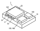
図1は本発明の一実施例に係る弾性波フィルタ(SAWフィルタ)の斜視図であり、(a)上面斜視図、(b)下面斜視図である。また図2はその回路ブロック図である。図3は弾性波フィルタを構成する多層基板の部分断面拡大図である。
多層基板10の内部には、電極パターン(ラインパターンやビアホール)で形成された接続線路70,80,85,90が形成され、多層基板10の上面部には弾性表面波素子(図示せず)が搭載され、この多層基板10の上面側に、弾性表面波素子を気密封止するエポキシ樹脂などの樹脂部材15を備えている。
弾性表面波素子の不平衡入力ポートや平衡出力ポートは、前記接続線路を介して矩形に形成された多層基板の底面に設けられた高周波端子(不平衡信号入力端子20a、平衡信号出力端子20c)と接続し、グランドポートは同様に接続線路とグランド電極50を介して多層基板の底面に設けられたグランド端子(20d)と接続する。前記グランド端子(20d)は、多層基板の対向する側面に、それぞれ形成された不平衡信号入力端子20aと平衡信号出力端子20cの間に配置されている。本実施例においては、グランド端子を帯状の電極パターンで形成しているが、他の高周波端子と同形状の電極パターンとし、複数の電極パターンを、平衡信号出力端子間を除く他の側面側等の異なる位置に設けて形成しても良い。
FIG. 1 is a perspective view of an acoustic wave filter (SAW filter) according to an embodiment of the present invention, where (a) is a top perspective view and (b) is a bottom perspective view. FIG. 2 is a block diagram of the circuit. FIG. 3 is an enlarged partial cross-sectional view of a multilayer substrate constituting the acoustic wave filter.
Inside the
The unbalanced input port and the balanced output port of the surface acoustic wave element are high-frequency terminals (unbalanced
本実施例で最も特徴的な部分は、平衡信号出力端子を多層基板の最も底面側に形成されたグランド電極と積層方向に重なり合わないように構成した点にある。なお最も底面側に形成されたグランド電極とは、多層基板の底面に最も近い電極パターン(ビアホールを除く)がグランド電極であることを意味する。
グランド電極は平衡信号出力端子と積層方向に重なり合わないが、絶縁層面に広がって形成されているため、その上層に設けられた伝送線路が実装基板の電極パターンと干渉するのを防ぐ。また平衡信号出力端子との重なりを除く構成によって、寄生容量の形成を抑え、位相特性が劣化することが無く、優れた電気的特性を得ることが出来る。
The most characteristic part of this embodiment is that the balanced signal output terminal is configured not to overlap the ground electrode formed on the bottom surface side of the multilayer substrate in the stacking direction. The ground electrode formed closest to the bottom surface means that the electrode pattern (excluding via holes) closest to the bottom surface of the multilayer substrate is the ground electrode.
Although the ground electrode does not overlap with the balanced signal output terminal in the stacking direction, the ground electrode is formed so as to spread over the insulating layer surface, thereby preventing the transmission line provided on the upper layer from interfering with the electrode pattern of the mounting substrate. In addition, the configuration excluding the overlap with the balanced signal output terminal can suppress the formation of parasitic capacitance, and the phase characteristics are not deteriorated, and excellent electrical characteristics can be obtained.
図4は無線通信器の高周波回路のブロック図であって、本発明の一実施例に係る複合部品を用いて構成されたものである。また図5は複合部品の等価回路図である。以下説明において幾つかの通信方式を例示するが、各通信方式の周波数帯域は表1に示す通りであって、送信・受信は無線通信器端末を基準にしている。本発明が利用される通信方式は、例示した通信システムにのみに限定されるものではなく、GPSや、他のCDMA方式等にも利用可能であり、本発明は利用する通信方式には何等限定されない。 FIG. 4 is a block diagram of a high-frequency circuit of a wireless communication device, which is configured using a composite part according to an embodiment of the present invention. FIG. 5 is an equivalent circuit diagram of the composite part. In the following description, several communication methods are exemplified, but the frequency bands of the respective communication methods are as shown in Table 1, and transmission / reception is based on the wireless communication device terminal. The communication system in which the present invention is used is not limited to the illustrated communication system, and can be used in GPS, other CDMA systems, and the present invention is not limited to any communication system. Not.

この複合部品は、4つの通信方式に用いられるものであって、周波数帯域f1の第1通信方式(例えばGSM850)、周波数帯域f2の第2通信方式(例えばDCS1800)、周波数帯域f3の第3通信方式(例えばDCS1900)、周波数帯域f4の第4通信方式(例えばUMTS)とに対応した高周波回路に用いられ、前記通信方式の送受信信号の伝送経路を切り替える電界効果トランジスタ(FET)を用いた高周波スイッチ回路と、前記高周波スイッチに接続される分波回路とローパスフィルタと弾性波フィルタを少なくとも有する。 This composite component is used for four communication systems, and includes a first communication system (for example, GSM850) in the frequency band f1, a second communication system (for example, DCS1800) in the frequency band f2, and a third communication in the frequency band f3. A high-frequency switch using a field effect transistor (FET) that is used in a high-frequency circuit corresponding to a communication system (for example, DCS1900) and a fourth communication system (for example, UMTS) in the frequency band f4, and switches transmission / reception signal transmission paths of the communication system A circuit, a branching circuit connected to the high-frequency switch, a low-pass filter, and an elastic wave filter.
前記高周波スイッチは、6つのポートを備えるSP5Tの高周波スイッチSWであり、その第1のポート(共通ポート)aには、ESD(electro−Static discharge;静電気放電)対策回路220を介してフィルタ回路110が接続される。第2のポートbにはフィルタ回路130と、整合回路186と、DCカットコンデンサC3(図1では図示せず)が接続される。第3のポートcにはDCカットコンデンサC2(図1では図示せず)と、フィルタ回路140と、整合回路187が接続される。第4のポートdには、分波回路120と、その分波回路120を構成するフィルタ回路120aの後段に、整合回路188と、弾性波フィルタ150とが接続される。分波回路120を構成するフィルタ回路120bには整合回路180と、弾性波フィルタ155とが接続される。第5のポートeには整合回路185と、弾性波フィルタ160が接続され、第6のポートfには整合回路190が接続される。
The high-frequency switch is an SP5T high-frequency switch SW having six ports, and the first port (common port) a is connected to the
フィルタ回路110は、第1通信システムの送信信号の第3次高調波成分を減衰させるローパスフィルタである。フィルタ回路130は、第1通信方式の送信信号を通過させるローパスフィルタである。バンドパスフィルタであってもよい。フィルタ回路140は、第2通信方式及び第3通信方式の送信信号を通過させるローパスフィルタである。この場合もバンドパスフィルタを用いても良い。弾性波フィルタ150が前記第1通信方式の受信信号を通過させるバンドパスフィルタであり、弾性波フィルタ150が前記第3通信方式の受信信号を通過させるバンドパスフィルタであり、前記弾性波フィルタ160が前記第2通信方式の受信信号を通過させるバンドパスフィルタである。本実施例においては、弾性波フィルタ150、155、160として不平衡入力−平衡出力型のSAWフィルタを用いている。
分波回路120は、前記第1通信方式の受信信号を通過させるローパスフィルタ120aと、前記第3通信方式の受信信号を通過させるハイパスフィルタ120bを並列に接続したものである。整合回路180、185、186、187、188、190は主としてインピーダンスマッチングのために用いられるが、高周波信号の位相調整のために用いられる場合もある。
The
The
図6は複合部品の外観斜視図であり、図7は複合部品に用いる多層基板10の分解斜視図であって、各層の構成を示している。
フィルタ回路110,130,140、分波回路120、及び整合回路180、185、186、187、188、190はインダクタとコンデンサで構成されており、これらは、誘電体層と、AgやCu等の金属や前記金属をベースとする合金を用いてなるペーストを所定の形状に形成した電極パターンとで形成される多層基板に、前記電極パターンやチップ部品として構成される。
FIG. 6 is an external perspective view of the composite component, and FIG. 7 is an exploded perspective view of the
The
以下多層基板の構成について説明する。多層基板は、複数の誘電体層を積層して構成してなり、分波回路及びローパスフィルタのコイル用パターンが主に形成された複数の第1誘電体層と、コンデンサ用パターンが主に形成された複数の第2誘電体層と、アース用パターンが主に形成された複数の第3誘電体層とを備えている。コイル用パターンとコンデンサ用パターンとを異なる誘電体層に形成しているが、同じ誘電体層に形成しても良い。なお本実施例では。コイル用パターンは抵抗を低減するため断面積を大きくするように、コンデンサ用パターンと比べて厚く形成している。 The configuration of the multilayer substrate will be described below. The multi-layer substrate is formed by laminating a plurality of dielectric layers, and a plurality of first dielectric layers mainly including a pattern for a demultiplexing circuit and a low-pass filter, and a capacitor pattern are mainly formed. A plurality of second dielectric layers and a plurality of third dielectric layers mainly formed with a grounding pattern. Although the coil pattern and the capacitor pattern are formed in different dielectric layers, they may be formed in the same dielectric layer. In the present embodiment. The coil pattern is formed thicker than the capacitor pattern so as to increase the cross-sectional area in order to reduce resistance.
第1〜第3誘電体層は、例えば誘電体セラミクスを、ドクターブレード法などの周知のシート化方法によってグリーンシート化したものであり、積層後焼結して一体化されるものである。多層基板を構成する誘電体セラミクスとしては、例えばAl,Si及びSrを主成分として、Ti,Bi,Cu,Mn,Na,Kなどを副成分とするセラミックス、Al,Si及びSrを主成分として、Ca,Pb,Na,Kなどを複成分とするセラミクス、Al,Mg,Si及びGdを含むセラミクス、Al,Si,Zr及びMg含むセラミクスが挙げられる。誘電体の誘電率は5〜15程度が好ましい。また誘電体セラミクスの他に、樹脂や、樹脂/セラミック複合材を用いて多層基板を構成することも可能である。さらにHTCC(高温同時焼成セラミック)技術により、Al2O3を主体とする多層基板内に、タングステンやモリブデン等の高温焼結可能な金属導体により電極パターンを形成しても良い。
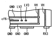
最下層のグリーンシート14の表面には、ほぼ全面を覆うアース用パターンGND(第1グランド電極)が形成されており、裏面には回路基板に実装するための端子電極が形成されている。前記端子電極は、各通信システム共通のアンテナポートANT(100a)と、第1の通信システムの送信信号が入力する第1送信ポートTX1(100b)と、第2、第3の通信システムの送信信号が入力する第2送信ポートTX2(100c)と、第1の通信システムが出力する受信ポートRX1(100d、100d2)と,第3の通信システムが出力する受信ポートRX2(100e1、100e2)と,第2の通信システムが出力する受信ポートRX3(100f1,100f2)と,第4の通信システムが入出力する送受信ポートTRX(100g)と、グランドポートGNDと、スイッチ回路制御用のコントロールポート(制御端子)V1,V2,V3,Vddを有し、それぞれがグリーンシートに形成されたビアホール(図中、黒丸、黒四角で表示)を介して上層のグリーンシート上の電極パターンと接続される。
The first to third dielectric layers are, for example, those obtained by forming dielectric ceramics into green sheets by a known sheet forming method such as a doctor blade method, and are integrated by sintering after lamination. As dielectric ceramics constituting the multilayer substrate, for example, Al, Si, and Sr as main components, Ti, Bi, Cu, Mn, Na, K, etc. as subcomponents, Al, Si, and Sr as main components. , Ca, Pb, Na, K and the like, ceramics containing Al, Mg, Si and Gd, ceramics containing Al, Si, Zr and Mg. The dielectric constant of the dielectric is preferably about 5-15. In addition to dielectric ceramics, it is also possible to form a multilayer substrate using a resin or a resin / ceramic composite material. Further, an electrode pattern may be formed by a high-temperature sinterable metal conductor such as tungsten or molybdenum in a multilayer substrate mainly composed of Al 2 O 3 by HTCC (high temperature co-fired ceramic) technology.
A ground pattern GND (first ground electrode) covering almost the entire surface is formed on the surface of the lowermost
本実施例では端子電極をLGA(Land Grid Array)としているが,BGA(Ball Grid Array)なども採用することができる。また本実施例では、制御端子V1,V2,V3,Vdd、受信系端子RX1、RX2、RX3、送信系端子TX1,TX2、アンテナ端子ANT及び送受信系端子TRXを、それぞれ異なると側面側に集めて配置している。このような配置によれば高周波スイッチモジュールが回路基板に実装されたときの他の高周波回路との接続を短く出来る。受信系端子RX1、RX2、RX3を一側面側に配置し、他の高周波端子や制御端子を配置しないことで、受信信号への影響を低減している。また受信信号の出力端に接地コンデンサが形成され無いように、端子電極とアース用パターンGNDとが重ならないようにした。このため、平衡出力される受信信号のフェイズバランスやアンプリチュードバランスを損なう事が無い。好ましくは、多層基板においてアース用パターンGND以外の電極パターンとも重ならないように構成する。
前記スイッチ回路制御用のコントロールポートV1,V2,V3,Vddは、多層基板の一側面に側に集められており、積層方向に連続するビアホールと、グリーンシート13上に並行して走るラインパターン(制御信号用線路)を介して前記第1の主面に形成された複数のデコーダ用実装電極と接続される。また同じ層にはフィルタ回路や整合回路を構成するコンデンサ用電極パターンが形成されている。
In this embodiment, the terminal electrode is an LGA (Land Grid Array), but a BGA (Ball Grid Array) or the like can also be adopted. In this embodiment, the control terminals V1, V2, V3, Vdd, the reception system terminals RX1, RX2, RX3, the transmission system terminals TX1, TX2, the antenna terminal ANT, and the transmission / reception system terminal TRX are collected on the side surface if they are different from each other. It is arranged. According to such an arrangement, when the high frequency switch module is mounted on the circuit board, the connection with other high frequency circuits can be shortened. The reception system terminals RX1, RX2, and RX3 are arranged on one side surface, and other high-frequency terminals and control terminals are not arranged, thereby reducing the influence on the reception signal. In addition, the terminal electrode and the ground pattern GND are not overlapped so that a ground capacitor is not formed at the output end of the received signal. For this reason, the phase balance and amplitude balance of the reception signal that is output in a balanced manner are not impaired. Preferably, the multilayer substrate is configured not to overlap with electrode patterns other than the ground pattern GND.
The control ports V1, V2, V3, and Vdd for controlling the switch circuit are gathered on one side of the multilayer substrate, and a via pattern that continues in the stacking direction and a line pattern that runs in parallel on the green sheet 13 ( The control signal lines are connected to a plurality of decoder mounting electrodes formed on the first main surface. In the same layer, a capacitor electrode pattern constituting a filter circuit and a matching circuit is formed.
グリーンシート12には、ほぼ全面を覆うアース用パターンGND(第2グランド電極)が形成されており、その一部は、電極が形成されてない抜き部となっている。前記抜き部には、制御信号用線路とFETスイッチの制御信号入力ポートとを接続するビアホールや、コンデンサ用電極パターンを他の層の電極パターンと接続するビアホールが形成されている。
The
グリーンシート11〜8には、フィルタ回路や整合回路を構成するインダクタ用電極パターンが形成されている。グリーンシート7には、コンデンサ用電極パターンとともに、ほぼ全面を覆うアース用パターンGND(第3グランド電極)が形成されている。コンデンサ用電極パターンは、信号の経路に直列に接続するコンデンサ用の電極パターンである。グリーンシート6〜4には、コンデンサ用電極パターンが形成され、そしてその上層のグリーンシート3には、コンデンサ用電極パターンGNDとともに、ほぼ全面を覆うアース用パターンGND(第4グランド電極)が形成されている。グリーンシート2には、グリーンシート1に形成された実装電極と、前記インダクタ用電極パターンや前記コンデンサ用電極パターンとの接続のための線路(電極パターン)が形成されている。
各電極パターンは適宜ビアホールを介して適宜接続され、得られた積層体を850℃〜1000℃程度(用いる導体や誘電体セラミクスによる)で焼結して多層基板とし、これにFETスイッチやSAWフィルタを実装して本発明に係るスイッチモジュールとした。
本実施例においては、更にDCカットコンデンサC1〜C3、ESD対策回路のインダクタL1、コンデンサC1(コンデンサC1はDCカットと共用)を積層基板上に実装している。なお、これらのインダクタやコンデンサを積層基板内に電極パターンで形成することも可能であるが、他の回路素子と比べて、比較的大きな容量値、インダクタンス値が必要となるので、専らチップ部品として積層基板上に実装する場合が多い。
The
Each electrode pattern is appropriately connected through a via hole, and the obtained laminated body is sintered at about 850 ° C. to 1000 ° C. (depending on the conductor and dielectric ceramic used) to form a multilayer substrate, and this is used as an FET switch or SAW filter. Was implemented as a switch module according to the present invention.
In this embodiment, DC cut capacitors C1 to C3, an inductor L1 of an ESD countermeasure circuit, and a capacitor C1 (capacitor C1 is also used for DC cut) are mounted on the multilayer substrate. Although it is possible to form these inductors and capacitors in the multilayer substrate with electrode patterns, they require relatively large capacitance values and inductance values compared to other circuit elements. It is often mounted on a multilayer substrate.
多層基板の上面にFETスイッチやSAWフィルタ、及びチップインダクタやチップコンデンサを実装するための実装電極の内、FETスイッチやSAWフィルタのグランド端子は、グリーンシート3に形成されたアース用パターンGNDとビアホールで接続される。またグリーンシート3に形成されたアース用パターンGNDは、グリーンシート7、12、14の各アース用パターンGNDと複数のビアホールで接続されている。
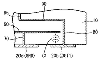
図8に多層基板10の部分断面拡大図を示す。前記SAWフィルタの平衡出力ポートと接続する実装電極は、多層基板の裏面に形成された高周波端子のうちの平衡出力端子RX3と、積層方向に連続する第1ビアホール群を介して接続されている。図示していないが他の平衡出力端子も同様に、それぞれが他の第1ビアホール群を介してSAWフィルタの平衡出力ポートと接続する。またグランド電極は平衡出力端子と積層方向に重なり合わない構成によりフェイズバランスやアンプリチュードバランス等の位相特性を損ねることが無い。更に前記第1ビアホール群と前記制御信号用線路との間には、面内に縦列し、積層方向に連続した第2ビアホール群が形成され、第1グランド電極〜第4グランド電極の間を接続している。このような構成により、ノイズの影響を受け易い受信信号の経路を、制御信号の経路、送信信号の経路から分離して配置することで、更に優れた挿入損失特性を得ることが出来た。
Of the mounting electrodes for mounting FET switches, SAW filters, chip inductors and chip capacitors on the upper surface of the multilayer substrate, the ground terminals of the FET switches and SAW filters are ground patterns GND and via holes formed on the
FIG. 8 is an enlarged partial sectional view of the
以上説明したように、本発明によれば、弾性波フィルタに用いる多層基板の構造に起因する位相特性の劣化を改善することが出来、電気的特性に優れた弾性波フィルタ及び複合部品を得ることが出来る。 As described above, according to the present invention, it is possible to improve the deterioration of the phase characteristics due to the structure of the multilayer substrate used for the elastic wave filter, and to obtain an elastic wave filter and a composite component having excellent electrical characteristics. I can do it.
10 多層基板
110,130,140 フィルタ回路
115 FETスイッチ
120 ESD対策回路
150,155,160 SAWフィルタ
180、185、186、187、190 整合回路
120 分波回路
DESCRIPTION OF
Claims (2)
前記スイッチング素子及び前記弾性波素子の下部であって、前記多層基板の内層には、異なる層に形成され、ビアホールを介して接続された複数のグランド電極を有し、前記グランド電極間には、前記分波回路を構成するリアクタンス素子用の電極パターンを含み、
前記高周波端子は少なくとも平衡信号端子と不平衡信号端子を有し、前記平衡信号端子は各弾性波素子の平衡ポートと前記多層基板に設けられた接続線路を介して接続し、前記多層基板の底面の一側面側にのみに並設され、
前記多層基板の内層において、前記平衡信号端子と積層方向に重なる部位には、前記接続線路のみが設けられ、前記グランド電極は、前記平衡信号端子と、前記多層基板の表面に形成された弾性波素子の平衡ポートと接続する実装電極とに積層方向に重なり合わないことを特徴とする高周波部品。 A balanced output elastic wave element and a switching element are mounted on the multilayer board, a ground terminal and a high frequency terminal are provided on the bottom surface of the multilayer board , and a branching circuit is connected to the high frequency switch circuit configured by the switching element. The wave circuit is connected to a plurality of elastic wave filters made of the elastic wave elements,
Below the switching element and the acoustic wave element, the inner layer of the multilayer substrate has a plurality of ground electrodes formed in different layers and connected via via holes, and between the ground electrodes, Including an electrode pattern for reactance elements constituting the branching circuit,
The high-frequency terminal has at least a balanced signal terminal and an unbalanced signal terminal, and the balanced signal terminal is connected to a balanced port of each acoustic wave element via a connection line provided on the multilayer substrate, and a bottom surface of the multilayer substrate. Are juxtaposed only on one side,
In the inner layer of the multilayer substrate, only the connection line is provided in a portion overlapping the balanced signal terminal in the stacking direction, and the ground electrode is an elastic wave formed on the surface of the balanced signal terminal and the multilayer substrate. high-frequency component, characterized in that on the mounting electrode connected to the balanced port of the elements do not overlap in the stacking direction.
Priority Applications (1)
| Application Number | Priority Date | Filing Date | Title |
|---|---|---|---|
| JP2007114657A JP5041285B2 (en) | 2007-04-24 | 2007-04-24 | High frequency components |
Applications Claiming Priority (1)
| Application Number | Priority Date | Filing Date | Title |
|---|---|---|---|
| JP2007114657A JP5041285B2 (en) | 2007-04-24 | 2007-04-24 | High frequency components |
Publications (3)
| Publication Number | Publication Date |
|---|---|
| JP2008271421A JP2008271421A (en) | 2008-11-06 |
| JP2008271421A5 JP2008271421A5 (en) | 2010-04-30 |
| JP5041285B2 true JP5041285B2 (en) | 2012-10-03 |
Family
ID=40050304
Family Applications (1)
| Application Number | Title | Priority Date | Filing Date |
|---|---|---|---|
| JP2007114657A Expired - Fee Related JP5041285B2 (en) | 2007-04-24 | 2007-04-24 | High frequency components |
Country Status (1)
| Country | Link |
|---|---|
| JP (1) | JP5041285B2 (en) |
Families Citing this family (8)
| Publication number | Priority date | Publication date | Assignee | Title |
|---|---|---|---|---|
| JP2009089165A (en) * | 2007-10-01 | 2009-04-23 | Murata Mfg Co Ltd | High-frequency module |
| JP5273861B2 (en) | 2009-04-22 | 2013-08-28 | 太陽誘電株式会社 | Communication module |
| DE112011102499T5 (en) | 2010-07-27 | 2013-06-20 | Murata Manufacturing Co., Ltd. | RF module |
| WO2018043206A1 (en) | 2016-09-05 | 2018-03-08 | 株式会社村田製作所 | Lc filter, high frequency front end circuit, and communication device |
| JP6661521B2 (en) | 2016-12-05 | 2020-03-11 | 太陽誘電株式会社 | Filters and multiplexers |
| WO2018168653A1 (en) * | 2017-03-14 | 2018-09-20 | 株式会社村田製作所 | High frequency module |
| WO2019150787A1 (en) | 2018-02-01 | 2019-08-08 | 株式会社村田製作所 | Filter module and high frequency module |
| JP7138198B2 (en) * | 2018-06-12 | 2022-09-15 | ケーエムダブリュ・インコーポレーテッド | Cavity filter and connecting structure contained therein |
Family Cites Families (16)
| Publication number | Priority date | Publication date | Assignee | Title |
|---|---|---|---|---|
| JP3869919B2 (en) * | 1997-11-05 | 2007-01-17 | Tdk株式会社 | Surface acoustic wave device |
| JP2002118487A (en) * | 2000-10-06 | 2002-04-19 | Matsushita Electric Ind Co Ltd | High-frequency composite switch module |
| JP4532825B2 (en) * | 2000-11-01 | 2010-08-25 | 日立金属株式会社 | High frequency switch module |
| JP3729396B2 (en) * | 2001-11-01 | 2005-12-21 | 日立金属株式会社 | High frequency components |
| JP2003304139A (en) * | 2002-02-07 | 2003-10-24 | Ngk Spark Plug Co Ltd | Package for surface acoustic wave branching filter and method for manufacturing the same package |
| JP3911426B2 (en) * | 2002-02-26 | 2007-05-09 | 京セラ株式会社 | Surface acoustic wave filter package and surface acoustic wave filter device |
| JP2004080233A (en) * | 2002-08-14 | 2004-03-11 | Murata Mfg Co Ltd | Branching filter |
| JP2004166258A (en) * | 2002-10-25 | 2004-06-10 | Hitachi Metals Ltd | Balanced/unbalanced multiband filter module |
| JP3967289B2 (en) * | 2003-04-30 | 2007-08-29 | 富士通メディアデバイス株式会社 | Duplexer and electronic device |
| JP4323972B2 (en) * | 2004-01-30 | 2009-09-02 | 三星電子株式会社 | Modulation circuit and modulation method |
| EP1729413B1 (en) * | 2004-03-16 | 2015-12-09 | Hitachi Metals, Ltd. | High-frequency circuit and high-frequency component |
| JP4412123B2 (en) * | 2004-09-09 | 2010-02-10 | エプソントヨコム株式会社 | Surface acoustic wave device |
| JP4091043B2 (en) * | 2004-12-22 | 2008-05-28 | 富士通メディアデバイス株式会社 | Duplexer |
| JP4601415B2 (en) * | 2004-12-24 | 2010-12-22 | 京セラ株式会社 | Surface acoustic wave device and communication device |
| WO2006070616A1 (en) * | 2004-12-28 | 2006-07-06 | Murata Manufacturing Co., Ltd. | Balance/unbalance filter module and communication apparatus |
| JP4446922B2 (en) * | 2005-04-21 | 2010-04-07 | 富士通メディアデバイス株式会社 | Filters and duplexers |
-
2007
- 2007-04-24 JP JP2007114657A patent/JP5041285B2/en not_active Expired - Fee Related
Also Published As
| Publication number | Publication date |
|---|---|
| JP2008271421A (en) | 2008-11-06 |
Similar Documents
| Publication | Publication Date | Title |
|---|---|---|
| JP4324807B2 (en) | High frequency switch module | |
| JP5316544B2 (en) | High frequency circuit, high frequency component, and multiband communication device | |
| JP5041285B2 (en) | High frequency components | |
| JP5029946B2 (en) | Switch module | |
| US7924118B2 (en) | Duplexer and elastic wave device | |
| JP2003198325A (en) | Branching filter and communication equipment | |
| JP5796579B2 (en) | Laminated electronic component with filter and balun | |
| JP5630697B2 (en) | Electronic components | |
| JP2001211097A (en) | High frequency switch module for multi-band | |
| JP2005268878A (en) | Antenna duplexer | |
| JP4702622B2 (en) | Switch module | |
| JP2010147589A (en) | High frequency circuit, high frequency component, and communication device | |
| JP3729396B2 (en) | High frequency components | |
| US20040012461A1 (en) | High-frequency device and communication apparatus | |
| JP2003142981A5 (en) | ||
| JP4936119B2 (en) | Multilayer balun transformer and high frequency components | |
| US11075658B2 (en) | Multilayer substrate, filter, multiplexer, radio-frequency front-end circuit, and communication device | |
| JP4678572B2 (en) | Multilayer balun transformer and high-frequency switch module using the same | |
| JP5549820B2 (en) | Triplexa | |
| JP4794247B2 (en) | High frequency module | |
| JP2006279553A (en) | High-frequency switching module and radio communication device | |
| WO2022230708A1 (en) | High-frequency circuit and communication device | |
| JP2005167624A (en) | Laminated electronic component and radio apparatus | |
| JP2009159412A (en) | High-frequency, component and communication device | |
| JP2010136288A (en) | Band pass filter, radio frequency component, and communication device |
Legal Events
| Date | Code | Title | Description |
|---|---|---|---|
| A521 | Request for written amendment filed |
Free format text: JAPANESE INTERMEDIATE CODE: A523 Effective date: 20100315 |
|
| A621 | Written request for application examination |
Free format text: JAPANESE INTERMEDIATE CODE: A621 Effective date: 20100315 |
|
| A977 | Report on retrieval |
Free format text: JAPANESE INTERMEDIATE CODE: A971007 Effective date: 20120201 |
|
| A131 | Notification of reasons for refusal |
Free format text: JAPANESE INTERMEDIATE CODE: A131 Effective date: 20120224 |
|
| A521 | Request for written amendment filed |
Free format text: JAPANESE INTERMEDIATE CODE: A523 Effective date: 20120424 |
|
| TRDD | Decision of grant or rejection written | ||
| A01 | Written decision to grant a patent or to grant a registration (utility model) |
Free format text: JAPANESE INTERMEDIATE CODE: A01 Effective date: 20120615 |
|
| A01 | Written decision to grant a patent or to grant a registration (utility model) |
Free format text: JAPANESE INTERMEDIATE CODE: A01 |
|
| A61 | First payment of annual fees (during grant procedure) |
Free format text: JAPANESE INTERMEDIATE CODE: A61 Effective date: 20120628 |
|
| R150 | Certificate of patent or registration of utility model |
Ref document number: 5041285 Country of ref document: JP Free format text: JAPANESE INTERMEDIATE CODE: R150 Free format text: JAPANESE INTERMEDIATE CODE: R150 |
|
| FPAY | Renewal fee payment (event date is renewal date of database) |
Free format text: PAYMENT UNTIL: 20150720 Year of fee payment: 3 |
|
| LAPS | Cancellation because of no payment of annual fees |