EP1182699A2 - Verfahren zur Bildung eines dicken dielektrischen Gebietes in einem Halbleitersubstrat - Google Patents
Verfahren zur Bildung eines dicken dielektrischen Gebietes in einem Halbleitersubstrat Download PDFInfo
- Publication number
- EP1182699A2 EP1182699A2 EP01117972A EP01117972A EP1182699A2 EP 1182699 A2 EP1182699 A2 EP 1182699A2 EP 01117972 A EP01117972 A EP 01117972A EP 01117972 A EP01117972 A EP 01117972A EP 1182699 A2 EP1182699 A2 EP 1182699A2
- Authority
- EP
- European Patent Office
- Prior art keywords
- trench
- substrate
- dielectric layer
- dielectric
- region
- Prior art date
- Legal status (The legal status is an assumption and is not a legal conclusion. Google has not performed a legal analysis and makes no representation as to the accuracy of the status listed.)
- Granted
Links
Images




Classifications
-
- H—ELECTRICITY
- H10—SEMICONDUCTOR DEVICES; ELECTRIC SOLID-STATE DEVICES NOT OTHERWISE PROVIDED FOR
- H10W—GENERIC PACKAGES, INTERCONNECTIONS, CONNECTORS OR OTHER CONSTRUCTIONAL DETAILS OF DEVICES COVERED BY CLASS H10
- H10W10/00—Isolation regions in semiconductor bodies between components of integrated devices
- H10W10/01—Manufacture or treatment
- H10W10/011—Manufacture or treatment of isolation regions comprising dielectric materials
- H10W10/014—Manufacture or treatment of isolation regions comprising dielectric materials using trench refilling with dielectric materials, e.g. shallow trench isolations
-
- H—ELECTRICITY
- H10—SEMICONDUCTOR DEVICES; ELECTRIC SOLID-STATE DEVICES NOT OTHERWISE PROVIDED FOR
- H10W—GENERIC PACKAGES, INTERCONNECTIONS, CONNECTORS OR OTHER CONSTRUCTIONAL DETAILS OF DEVICES COVERED BY CLASS H10
- H10W10/00—Isolation regions in semiconductor bodies between components of integrated devices
- H10W10/01—Manufacture or treatment
- H10W10/021—Manufacture or treatment of air gaps
-
- H—ELECTRICITY
- H10—SEMICONDUCTOR DEVICES; ELECTRIC SOLID-STATE DEVICES NOT OTHERWISE PROVIDED FOR
- H10W—GENERIC PACKAGES, INTERCONNECTIONS, CONNECTORS OR OTHER CONSTRUCTIONAL DETAILS OF DEVICES COVERED BY CLASS H10
- H10W10/00—Isolation regions in semiconductor bodies between components of integrated devices
- H10W10/10—Isolation regions comprising dielectric materials
- H10W10/17—Isolation regions comprising dielectric materials formed using trench refilling with dielectric materials, e.g. shallow trench isolations
-
- H—ELECTRICITY
- H10—SEMICONDUCTOR DEVICES; ELECTRIC SOLID-STATE DEVICES NOT OTHERWISE PROVIDED FOR
- H10W—GENERIC PACKAGES, INTERCONNECTIONS, CONNECTORS OR OTHER CONSTRUCTIONAL DETAILS OF DEVICES COVERED BY CLASS H10
- H10W10/00—Isolation regions in semiconductor bodies between components of integrated devices
- H10W10/20—Air gaps
Definitions
- the present patent application relates to a method for Formation of a dielectric region in a semiconductor substrate.
- the electrical performance more integrated, more passive Components such as polysilicon resistors, polysilicon-polysilicon or metal-metal capacities as well Coils are often caused by parasitic capacitive couplings deteriorated the semiconductor substrate used. This occurs especially on when semiconductor substrates with lower Conductivity can be used. Capacitive substrate coupling can cause a drastic deterioration of high frequency components to lead.
- a dielectric insulating layer be arranged locally under the components to be isolated. The thicker the dielectric layer is, the better the decoupling of the components from that Substrate. There are already different ways to produce thick layers of insulation.
- organic spin-on layers like Polyamide can be used.
- these materials can because of their temperature sensitivity only at the end of the process be used.
- these layers have the Disadvantage that due to the large layer thickness of about 10 complicated by a subsequent high-resolution structuring becomes. This means that these layers only can be used to isolate the last metal level, in which the contact hole openings to the underlying one Layers can be formed without fine structuring and consequently occupy a large proportion of the substrate surface.
- the invention first forms the first and the second trench, with a bridge between the two trenches arises. If it is provided that a relatively large area the substrate surface with a dielectric region is to be provided, for example a whole series of Trenches with ridges in between.
- the trenches can be formed with a depth that is later Corresponds to the thickness of the dielectric region.
- the trenches are first filled with the first dielectric layer, only one layer thickness has to be deposited, which corresponds approximately to half the trench width. This process is compared to a thick layer thickness of the dielectric Shift quickly and very inexpensively. Below is a land between the deposited first dielectric Removed layer, creating a third trench.
- the third trench is formed for example with a depth which is roughly the depth of the first trench previously formed and so that the filling depth corresponds to the first dielectric layer.
- the first dielectric layer is planarized.
- this procedure has the advantage that Planarization step of the web between the first and the second trench is exposed and in a subsequent one Etching step can be removed.
- the planarization step also has the advantage that a topological level between the surface of the semiconductor substrate and the dielectric Area is avoided.
- Another embodiment of the method according to the invention provides that the web by an isotropic or by a anisotropic etching is removed. Since the bridge between two trenches filled with dielectric material are arranged, can the web by an isotropic etching, which selectively Bridge against the dielectric layer in the first and the second trench removed, etched. Is also one anisotropic etching possible, for example RIE (Reactive Ion Etch) used to against a paint mask, against a hard mask or against the material difference from web to dielectric Layer is selective.
- RIE Reactive Ion Etch
- a hard mask is used for the formation of the first trench .
- the use of a hard mask has the advantage that the first trench or second trench with a large trench depth can.
- the paint mask for isotropic etching serve a window Expose in which the web is arranged, so that the rest Substrate is protected from the etching.
- Another embodiment of the method according to the invention provides that the first dielectric layer in an upper Area of the first trench is formed and in a lower one Area located below the top area is, a cavity is created.
- the cavity has the advantage that an improved decoupling between the substrate and the Component is reached.
- the second dielectric Layer formed in an upper area of the third trench will and in a lower area that is below the upper one Area is arranged, a second cavity is formed.
- the second cavity has the advantage that the decoupling between the substrate and the device is further improved.
- first cavity and the second cavity are formed contiguously.
- the contiguous Formation of the first and second cavities has the advantage that an improved decoupling between the substrate and one disposed on the dielectric region Component is reached.
- a substrate 1 is shown in which a trench isolation 2 is arranged.
- the trench isolation 2 is, for example, by depositing an insulation layer 3 have been formed on the surface of the substrate 1.
- Farther A region 17 of the semiconductor substrate 1 is shown.
- the insulation layer 3 of the Surface of the substrate 1 has been removed, the surface of the substrate 1, for example with a CMP (Chemical Mechanical Polishing) step has been planarized.
- a mask 4 is arranged on the surface of the substrate 1, which is structured.
- a subsequent process step according to FIG. 3 sees the formation a first trench 5 and a second trench 7, wherein between the first trench 5 and the second trench 7 a web 6 remains.
- the web 6 is, for example, with the mask 4 masked so that the formation of the first trench 5 and the second trench 7 performed etching step Trench 6 leaves.
- the etch to form the first trench 5 and the second trench 7 becomes anisotropic, for example performed a trench with high aspect ratio (Trench depth to trench diameter).
- the ditch can, for example, with a RIE (Reactive Ion Etch) step be formed.
- the substrate 1 is made of silicon, for example educated.
- the trench isolation 2 is an STI (Shallow Trench insulation) is formed and is made of silicon oxide, for example or a doped silicon oxide or silicate glass educated.
- the mask 4 is formed as a hard mask and can contain, for example, silicon oxide or silicon nitride.
- a CVD (Chemical Vaper Deposition) process be used.
- the first dielectric layer can contain silicon oxide or silicon nitride, for example.
- the surface of the substrate 1 is so processed that the first dielectric layer 8 and the Mask 4 are removed from the surface of the substrate 1. This can be done, for example, using a CMP step become.
- the CMP step also has the advantage that the surface of the substrate 1 is planarized. advantageously, planarization is pushed so far that the surface of the web 6 is exposed.
- an uncritical mask 40 is arranged so that for example, it overlaps the trench insulation 2 and thus exposes the substrate 1 in an area in which a dielectric Area 11 is to be formed, and in one area protects in which active components can be formed.
- On the uncritical mask 40 does not become high resolution lithographic Conditions are met because the trench isolation 2 is roughly structured.
- the web 6 is then removed. This is for example with an anisotropic or isotropic etching possible. The etching can, for example self-aligned to those already in the first trench 5 and the second trench 7 existing oxide webs from the first dielectric layer 8 exist.
- the uncritical mask 40 is removed and a second dielectric layer 10 on the surface of the substrate 1 and on the first dielectric layer in the first trench 5 and the second trench 7 are formed.
- the second dielectric layer 10 can, for example, with a CVD process to be separated.
- the third trench 9 filled up, for example. For this, a layer thickness for the second dielectric layer 10, which is approximately the same half the trench width of the third trench 9 corresponds.
- a CMP step is performed which the surface of the substrate 1 is planarized and the second dielectric layer 10 from the surface of the substrate 1 away.
- the first dielectric layer 8 and the second dielectric layer 10 form a dielectric region 11.
- the second dielectric layer 10 can also be silicon oxide or contain silicon nitride.
- a process variant is shown with reference to FIG. 9, which follows on from Figure 6. It is envisaged that the third trench 9 is not completely filled, but a first cavity 12 in the area of the third trench 9 is formed.
- the Cavity 12 arises from the fact that the second dielectric Layer 10 formed with reduced edge coverage the trench 9 is closed in its upper region is before the trench 9 is completely filled.
- the relative Dielectric constant of a cavity is in the Order of magnitude 1, which is an improvement over the material the first dielectric layer and the second dielectric layer Layer can represent.
- the first dielectric exists Layer of silicon oxide, for example, it points a relative dielectric constant of 4. Thereby the decoupling of components is improved, which on the dielectric region are formed.
- a deposition process can be used for this, which has a reduced edge coverage, so that the first Trench 5 in its upper area is closed before the first trench 5 is completely filled, so that the second cavity 14 in the lower region of the trench 5 forms.
- the relative dielectric constant of the cavity is on the order of 1, compared to a silicon oxide with a relative dielectric constant of about 4 represents an improvement.
- the surface of the substrate 1 etched back and planarized, the first dielectric Layer 8 is partially removed again. Then will an uncritical mask 40 on the surface of the substrate arranged, for example, the trench isolation 2 partially overlaps.
- a deposition process is used which has a reduced edge coverage has, so that between the free-floating Structures of the first dielectric layer 8 the second dielectric layer 10 is formed.
- Figure 16 shows a plan view of a substrate 1, the one closed ring as trench insulation 2.
- FIG. 17 shows a top view according to FIG. 16, at that in the inner surface surrounded by the trench insulation 2 a first trench 5, a web 6 and a second trench 7 is formed, the web 6 between the first trench 5 and the second trench 7 is arranged.
Landscapes
- Element Separation (AREA)
- Semiconductor Integrated Circuits (AREA)
Abstract
Description
- Bilden eines ersten Grabens und eines zweiten Grabens in dem Bereich des Halbleitersubstrats, wobei ein Steg zwischen dem ersten Graben und dem zweiten Graben gebildet wird;
- Bilden einer ersten dielektrischen Schicht in dem ersten und dem zweiten Graben;
- Entfernen des Stegs, wodurch ein dritter Graben entsteht;
- Bilden einer zweiten dielektrischen Schicht in dem dritten Graben.
- Figur 1
- ein Substrat mit einem Isolationsgraben;
- Figur 2
- ein Substrat gemäß Figur 1, auf dem eine Maske gebildet ist;
- Figur 3
- ein Substrat gemäß Figur 2, wobei die Maske zur Ätzung von Gräben verwendet wurde;
- Figur 4
- ein Substrat gemäß Figur 3, wobei die Gräben mit einer dielektrischen Schicht gefüllt sind;
- Figur 5
- ein Substrat gemäß Figur 4, wobei die Substratoberfläche planarisiert ist;
- Figur 6
- das Substrat aus Figur 5, wobei ein Steg zwischen den dielektrischen Schichten herausgeätzt wurde und ein Graben gebildet wurde;
- Figur 7
- das Substrat gemäß Figur 6, wobei eine zweite dielektrische Schicht auf dem Substrat und in einem Graben angeordnet ist;
- Figur 8
- das Substrat gemäß Figur 7, wobei die erste dielektrische Schicht und die zweite dielektrische Schicht als dielektrisches Gebiet dargestellt sind;
- Figur 9
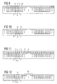
- eine Prozeßvariante, die sich an Figur 6 anschließt, wobei eine zweite dielektrische Schicht auf dem Substrat abgeschieden wird, und ein Hohlraum gebildet wird;
- Figur 10
- das Substrat gemäß Figur 9, wobei die Substratoberfläche planarisiert ist;
- Figur 11
- eine Prozeßvariante, die sich an Figur 3 anschließt, wobei eine erste dielektrische Schicht auf der Substratoberfläche abgeschieden wird und einen Hohlraum in dem Substrat in einem der vorher geätzten Gräben bildet;
- Figur 12
- das Substrat gemäß Figur 11, wobei die Substratoberfläche planarisiert wurde;
- Figur 13
- das Substrat gemäß Figur 12, wobei ein Steg, der zwischen zwei Gräben angeordnet war, entfernt wurde;
- Figur 14
- ein Substrat nach Figur 13, wobei eine zweite dielektrische Schicht auf der Substratoberfläche abgeschieden ist und in dem Substrat ein Hohlraum gebildet ist;
- Figur 15
- ein Substrat gemäß Figur 14, wobei die erste dielektrische Schicht und die zweite dielektrische Schicht eine dielektrische Membran bilden, die einen Hohlraum überspannt;
- Figur 16
- die Draufsicht auf ein Substrat, wobei eine Grabenisolation angeordnet ist;
- Figur 17
- das Substrat aus Figur 16, wobei ein erster Graben, ein Steg und ein zweiter Graben dargestellt sind.
Claims (8)
- Verfahren zur Bildung eines dielektrischen Gebiets in einem Bereich (17) eines Halbleitersubstrats (1) mit den Schritten:Bilden eines ersten Grabens (5) und eines zweiten Grabens (7) in dem Bereich (17) des Halbleitersubstrats (1), wobei ein Steg (6) zwischen dem ersten Graben (5) und dem zweiten Graben (7) gebildet wird;Bilden einer ersten dielektrischen Schicht (8) in dem ersten Graben (5) und dem zweiten Graben (7);Entfernen des Stegs (6), wodurch ein dritter Graben (9) entsteht;Bilden einer zweiten dielektrischen Schicht (10) in dem dritten Graben (9).
- Verfahren nach Anspruch 1,
dadurch gekennzeichnet, daß
die erste dielektrische Schicht (8) planarisiert wird. - Verfahren nach einem der Ansprüche 1 oder 2,
dadurch gekennzeichnet, daß
der Steg (6) durch eine isotrope oder eine anisotrope Ätzung entfernt wird. - Verfahren nach einem der Ansprüche 1 bis 3,
dadurch gekennzeichnet, daß
zur Bildung des ersten Grabens (5) eine Maske (4) verwendet wird. - Verfahren nach einem der Ansprüche 1 bis 4,
dadurch gekennzeichnet, daß
zur Bildung des dritten Grabens (9) eine Lackmaske oder eine Hartmaske verwendet wird. - Verfahren nach einem der Ansprüche 1 bis 5,
dadurch gekennzeichnet, daß
die erste dielektrische Schicht (8) in einem oberen Bereich des ersten Grabens (5) gebildet wird und in einem unteren Bereich des ersten Grabens (5), der unterhalb des oberen Bereichs des ersten Grabens (5) angeordnet ist, ein Hohlraum (12) gebildet wird. - Verfahren nach einem der Ansprüche 1 bis 6,
dadurch gekennzeichnet, daß
die zweite dielektrische Schicht (10) in einem oberen Bereich des dritten Grabens (9) gebildet wird und in einem unteren Bereich des dritten Grabens (9), der unterhalb des oberen Bereichs des dritten Grabens (9) angeordnet ist, ein zweiter Hohlraum (14) gebildet wird. - Verfahren nach Anspruch 7,
dadurch gekennzeichnet, daß
der erste Hohlraum (12) und der zweite Hohlraum (14) zusammenhängend ausgebildet werden.
Applications Claiming Priority (2)
| Application Number | Priority Date | Filing Date | Title |
|---|---|---|---|
| DE10041084A DE10041084A1 (de) | 2000-08-22 | 2000-08-22 | Verfahren zur Bildung eines dielektrischen Gebiets in einem Halbleitersubstrat |
| DE10041084 | 2000-08-22 |
Publications (3)
| Publication Number | Publication Date |
|---|---|
| EP1182699A2 true EP1182699A2 (de) | 2002-02-27 |
| EP1182699A3 EP1182699A3 (de) | 2007-01-31 |
| EP1182699B1 EP1182699B1 (de) | 2010-09-01 |
Family
ID=7653317
Family Applications (1)
| Application Number | Title | Priority Date | Filing Date |
|---|---|---|---|
| EP01117972A Expired - Lifetime EP1182699B1 (de) | 2000-08-22 | 2001-07-24 | Verfahren zur Bildung eines dicken dielektrischen Gebietes in einem Halbleitersubstrat |
Country Status (3)
| Country | Link |
|---|---|
| US (1) | US6613644B2 (de) |
| EP (1) | EP1182699B1 (de) |
| DE (2) | DE10041084A1 (de) |
Families Citing this family (22)
| Publication number | Priority date | Publication date | Assignee | Title |
|---|---|---|---|---|
| ITTO20011038A1 (it) * | 2001-10-30 | 2003-04-30 | St Microelectronics Srl | Procedimento per la fabbricazione di una fetta semiconduttrice integrante dispositivi elettronici e una struttura per il disaccoppiamento el |
| FR2847382A1 (fr) * | 2002-11-19 | 2004-05-21 | St Microelectronics Sa | Realisation de tranchees fines et rapprochees |
| US7023069B2 (en) * | 2003-12-19 | 2006-04-04 | Third Dimension (3D) Semiconductor, Inc. | Method for forming thick dielectric regions using etched trenches |
| KR101250364B1 (ko) * | 2004-12-13 | 2013-04-05 | 세파론 오스트레일리아 (브이아이씨) 피티와이 엘티디 | 오스테오프로테게린 변이체 단백질 |
| TWI401749B (zh) * | 2004-12-27 | 2013-07-11 | 3D半導體股份有限公司 | 用於高電壓超接面終止之方法 |
| US7439583B2 (en) * | 2004-12-27 | 2008-10-21 | Third Dimension (3D) Semiconductor, Inc. | Tungsten plug drain extension |
| EP1872396A4 (de) * | 2005-04-22 | 2009-09-23 | Icemos Technology Corp | Superübergangsbauelement mit oxidausgekleideten gräben und verfahren zur herstellung eines superübergangsbauelements mit oxidausgekleideten gräben |
| US7446018B2 (en) | 2005-08-22 | 2008-11-04 | Icemos Technology Corporation | Bonded-wafer superjunction semiconductor device |
| US7429772B2 (en) | 2006-04-27 | 2008-09-30 | Icemos Technology Corporation | Technique for stable processing of thin/fragile substrates |
| KR100876806B1 (ko) * | 2006-07-20 | 2009-01-07 | 주식회사 하이닉스반도체 | 이중 패터닝 기술을 이용한 반도체 소자의 트랜지스터 형성방법 |
| US8580651B2 (en) * | 2007-04-23 | 2013-11-12 | Icemos Technology Ltd. | Methods for manufacturing a trench type semiconductor device having a thermally sensitive refill material |
| US7723172B2 (en) | 2007-04-23 | 2010-05-25 | Icemos Technology Ltd. | Methods for manufacturing a trench type semiconductor device having a thermally sensitive refill material |
| US20090085148A1 (en) * | 2007-09-28 | 2009-04-02 | Icemos Technology Corporation | Multi-directional trenching of a plurality of dies in manufacturing superjunction devices |
| US7777295B2 (en) * | 2007-12-11 | 2010-08-17 | Hvvi Semiconductors, Inc. | Semiconductor structure and method of manufacture |
| US7811896B2 (en) | 2007-12-11 | 2010-10-12 | Hvvi Semiconductors, Inc. | Semiconductor structure and method of manufacture |
| US20100230776A1 (en) * | 2007-12-11 | 2010-09-16 | Bishnu Prasanna Gogoi | Semiconductor structure and method of manufacture |
| US7846821B2 (en) | 2008-02-13 | 2010-12-07 | Icemos Technology Ltd. | Multi-angle rotation for ion implantation of trenches in superjunction devices |
| US7871895B2 (en) * | 2008-02-19 | 2011-01-18 | International Business Machines Corporation | Method and structure for relieving transistor performance degradation due to shallow trench isolation induced stress |
| US8030133B2 (en) * | 2008-03-28 | 2011-10-04 | Icemos Technology Ltd. | Method of fabricating a bonded wafer substrate for use in MEMS structures |
| US8501578B2 (en) * | 2010-01-22 | 2013-08-06 | Estivation Properties Llc | Semiconductor structure formed without requiring thermal oxidation |
| US8946814B2 (en) | 2012-04-05 | 2015-02-03 | Icemos Technology Ltd. | Superjunction devices having narrow surface layout of terminal structures, buried contact regions and trench gates |
| US9576842B2 (en) | 2012-12-10 | 2017-02-21 | Icemos Technology, Ltd. | Grass removal in patterned cavity etching |
Family Cites Families (24)
| Publication number | Priority date | Publication date | Assignee | Title |
|---|---|---|---|---|
| US4211582A (en) * | 1979-06-28 | 1980-07-08 | International Business Machines Corporation | Process for making large area isolation trenches utilizing a two-step selective etching technique |
| JPS5931215B2 (ja) * | 1980-05-15 | 1984-07-31 | 松下電器産業株式会社 | 絶縁層の形成方法 |
| JPS5842251A (ja) * | 1981-09-07 | 1983-03-11 | Toshiba Corp | 半導体装置の製造方法 |
| US5943578A (en) * | 1993-02-05 | 1999-08-24 | Kabushiki Kaisha Toshiba | Method of manufacturing a semiconductor device having an element isolating region |
| US5563343A (en) * | 1993-05-26 | 1996-10-08 | Cornell Research Foundation, Inc. | Microelectromechanical lateral accelerometer |
| JP3252569B2 (ja) * | 1993-11-09 | 2002-02-04 | 株式会社デンソー | 絶縁分離基板及びそれを用いた半導体装置及びその製造方法 |
| KR960014452B1 (ko) * | 1993-12-22 | 1996-10-15 | 금성일렉트론 주식회사 | 반도체 소자분리 방법 |
| US5516720A (en) * | 1994-02-14 | 1996-05-14 | United Microelectronics Corporation | Stress relaxation in dielectric before metallization |
| US5665622A (en) * | 1995-03-15 | 1997-09-09 | International Business Machines Corporation | Folded trench and rie/deposition process for high-value capacitors |
| US5665633A (en) * | 1995-04-06 | 1997-09-09 | Motorola, Inc. | Process for forming a semiconductor device having field isolation |
| US5926713A (en) * | 1996-04-17 | 1999-07-20 | Advanced Micro Devices, Inc. | Method for achieving global planarization by forming minimum mesas in large field areas |
| SE510443C2 (sv) * | 1996-05-31 | 1999-05-25 | Ericsson Telefon Ab L M | Induktorer för integrerade kretsar |
| DE69738012T2 (de) * | 1996-11-26 | 2007-12-13 | Matsushita Electric Industrial Co., Ltd., Kadoma | Halbleitervorrichtung und deren Herstellungsverfahren |
| EP0887847A1 (de) * | 1997-04-15 | 1998-12-30 | STMicroelectronics S.r.l. | Verfahren zur abschliessenden Passivierung integrierter Schaltungen |
| US5834359A (en) * | 1997-08-29 | 1998-11-10 | Vanguard International Semiconductor Corporation | Method of forming an isolation region in a semiconductor substrate |
| KR100280487B1 (ko) * | 1998-06-05 | 2001-03-02 | 김영환 | 반도체소자에서의소자격리구조및그격리방법 |
| EP0996149A1 (de) * | 1998-10-23 | 2000-04-26 | STMicroelectronics S.r.l. | Herstellungsverfahren für eine Oxidschicht mit grosser Dicke |
| JP2000183149A (ja) * | 1998-12-10 | 2000-06-30 | Sanyo Electric Co Ltd | 半導体装置 |
| JP3443358B2 (ja) * | 1999-03-24 | 2003-09-02 | シャープ株式会社 | 半導体装置の製造方法 |
| US6204149B1 (en) * | 1999-05-26 | 2001-03-20 | Micron Technology, Inc. | Methods of forming polished material and methods of forming isolation regions |
| US6482716B1 (en) * | 2000-01-11 | 2002-11-19 | Infineon Technologies North America Corp. | Uniform recess depth of recessed resist layers in trench structure |
| US6380078B1 (en) * | 2000-05-11 | 2002-04-30 | Conexant Systems, Inc. | Method for fabrication of damascene interconnects and related structures |
| US6391792B1 (en) * | 2000-05-18 | 2002-05-21 | Taiwan Semiconductor Manufacturing Co., Ltd | Multi-step chemical mechanical polish (CMP) planarizing method for forming patterned planarized aperture fill layer |
| US6444517B1 (en) * | 2002-01-23 | 2002-09-03 | Taiwan Semiconductor Manufacturing Company | High Q inductor with Cu damascene via/trench etching simultaneous module |
-
2000
- 2000-08-22 DE DE10041084A patent/DE10041084A1/de not_active Withdrawn
-
2001
- 2001-07-24 EP EP01117972A patent/EP1182699B1/de not_active Expired - Lifetime
- 2001-07-24 DE DE50115612T patent/DE50115612D1/de not_active Expired - Lifetime
- 2001-08-22 US US09/935,560 patent/US6613644B2/en not_active Expired - Lifetime
Also Published As
| Publication number | Publication date |
|---|---|
| EP1182699B1 (de) | 2010-09-01 |
| DE50115612D1 (de) | 2010-10-14 |
| US20020052092A1 (en) | 2002-05-02 |
| DE10041084A1 (de) | 2002-03-14 |
| EP1182699A3 (de) | 2007-01-31 |
| US6613644B2 (en) | 2003-09-02 |
Similar Documents
| Publication | Publication Date | Title |
|---|---|---|
| EP1182699B1 (de) | Verfahren zur Bildung eines dicken dielektrischen Gebietes in einem Halbleitersubstrat | |
| DE10065013B4 (de) | Verfahren zum Herstellen eines mikromechanischen Bauelements | |
| DE4125221C2 (de) | ||
| DE68927353T2 (de) | Verfahren zur Herstellung einer Planarisolierung | |
| DE69824481T2 (de) | Verfahren zur Herstellung von FET-Bauelementen mit flacher,maskenloser Grabenisolation | |
| DE69836943T2 (de) | Planarisierung von einer nicht-konformen Vorrichtungsschicht in Halbleiterherstellung | |
| DE19704149B4 (de) | Verfahren zum Herstellen einer Metallverdrahtung an einem Halbleiterbauteil sowie nach diesem Verfahren hergestellte Metallverdrahtung | |
| DE19906030A1 (de) | Grabenisolationsstruktur eines Halbleiterbauteils und Verfahren zum Herstellen einer Grabenisolationsstruktur mit Polysiliziumkontakt | |
| DE102014103341A1 (de) | Halbleiterbauelemente und Verfahren zu ihrer Bildung | |
| DE102005010944A1 (de) | Verfahren zur Herstellung eines Trägerscheibenkontaktes in grabenisolierten integrierten SOI Schaltungen mit Hochspannungsbauelementen | |
| DE19921110A1 (de) | Verfahren zur Herstellung eines Halbleiterbauelements | |
| DE10109564A1 (de) | Grabenkondensator und Verfahren zu seiner Herstellung | |
| DE4341171A1 (de) | Verfahren zur Herstellung einer integrierten Schaltungsanordnung | |
| DE10054190A1 (de) | Verfahren zum Einebnen einer Isolierung in Form eines flachen Grabens | |
| DE19840385C2 (de) | Verfahren zm Isolieren von Bereichen eines integrierten Schaltkreises und Halbleiterbaustein mit integriertem Schaltkreis | |
| DE19538005A1 (de) | Verfahren zum Erzeugen einer Grabenisolation in einem Substrat | |
| WO1999016125A1 (de) | Verfahren zur ausbildung einer grabenstruktur in einem siliziumsubstrat | |
| DE102006054334B3 (de) | Verfahren zur Herstellung eines Halbleiterbauelementes mit Isolationsgraben und Kontaktgraben | |
| DE10138510B4 (de) | Grabenisolation mit selbstjustierender Oberflächenversiegelung und Verfahren zur Herstellung einer solchen Grabenisolation | |
| DE10310080A1 (de) | Neuartiges Verfahren zum Ausbilden tieferer Gräben unabhängig von lithografisch bedingten, kritischen Abmessungen | |
| DE19843160B4 (de) | Halbleitervorrichtung mit Grabentrennung und Verfahren zu dessen Herstellung mittels Vorplanarisierung | |
| EP0914678B1 (de) | Verfahren zum auffüllen von gräben in einem substrat | |
| DE10335071B4 (de) | Verfahren zur Integrierung einer Ausrichtmarkierung und Grabenvorrichtung | |
| DE102006036076B4 (de) | Verfahren zum Herstellen eines Kondensatorbauelements | |
| DE19938481B4 (de) | Neue Technologie zur Bildung eines flaschenförmigen Tiefgrabens |
Legal Events
| Date | Code | Title | Description |
|---|---|---|---|
| PUAI | Public reference made under article 153(3) epc to a published international application that has entered the european phase |
Free format text: ORIGINAL CODE: 0009012 |
|
| AK | Designated contracting states |
Kind code of ref document: A2 Designated state(s): AT BE CH CY DE DK ES FI FR GB GR IE IT LI LU MC NL PT SE TR |
|
| AX | Request for extension of the european patent |
Free format text: AL;LT;LV;MK;RO;SI |
|
| PUAL | Search report despatched |
Free format text: ORIGINAL CODE: 0009013 |
|
| RIC1 | Information provided on ipc code assigned before grant |
Ipc: H01L 21/311 20060101ALI20061221BHEP Ipc: H01L 27/08 20060101ALN20061221BHEP Ipc: H01L 21/762 20060101AFI20061221BHEP Ipc: H01L 29/06 20060101ALN20061221BHEP Ipc: H01L 21/764 20060101ALI20061221BHEP |
|
| AK | Designated contracting states |
Kind code of ref document: A3 Designated state(s): AT BE CH CY DE DK ES FI FR GB GR IE IT LI LU MC NL PT SE TR |
|
| AX | Request for extension of the european patent |
Extension state: AL LT LV MK RO SI |
|
| 17P | Request for examination filed |
Effective date: 20070313 |
|
| 17Q | First examination report despatched |
Effective date: 20070516 |
|
| AKX | Designation fees paid |
Designated state(s): DE |
|
| RAP1 | Party data changed (applicant data changed or rights of an application transferred) |
Owner name: INFINEON TECHNOLOGIES AG |
|
| GRAP | Despatch of communication of intention to grant a patent |
Free format text: ORIGINAL CODE: EPIDOSNIGR1 |
|
| GRAS | Grant fee paid |
Free format text: ORIGINAL CODE: EPIDOSNIGR3 |
|
| GRAA | (expected) grant |
Free format text: ORIGINAL CODE: 0009210 |
|
| AK | Designated contracting states |
Kind code of ref document: B1 Designated state(s): DE |
|
| REF | Corresponds to: |
Ref document number: 50115612 Country of ref document: DE Date of ref document: 20101014 Kind code of ref document: P |
|
| PLBE | No opposition filed within time limit |
Free format text: ORIGINAL CODE: 0009261 |
|
| STAA | Information on the status of an ep patent application or granted ep patent |
Free format text: STATUS: NO OPPOSITION FILED WITHIN TIME LIMIT |
|
| 26N | No opposition filed |
Effective date: 20110606 |
|
| REG | Reference to a national code |
Ref country code: DE Ref legal event code: R097 Ref document number: 50115612 Country of ref document: DE Effective date: 20110606 |
|
| PGFP | Annual fee paid to national office [announced via postgrant information from national office to epo] |
Ref country code: DE Payment date: 20170912 Year of fee payment: 17 |
|
| REG | Reference to a national code |
Ref country code: DE Ref legal event code: R119 Ref document number: 50115612 Country of ref document: DE |
|
| PG25 | Lapsed in a contracting state [announced via postgrant information from national office to epo] |
Ref country code: DE Free format text: LAPSE BECAUSE OF NON-PAYMENT OF DUE FEES Effective date: 20190201 |