EP1177628B1 - Schaltungsanordnung zur erzeugung von strompulsen im versorgungsstrom integrierter schaltungen - Google Patents
Schaltungsanordnung zur erzeugung von strompulsen im versorgungsstrom integrierter schaltungen Download PDFInfo
- Publication number
- EP1177628B1 EP1177628B1 EP00931090A EP00931090A EP1177628B1 EP 1177628 B1 EP1177628 B1 EP 1177628B1 EP 00931090 A EP00931090 A EP 00931090A EP 00931090 A EP00931090 A EP 00931090A EP 1177628 B1 EP1177628 B1 EP 1177628B1
- Authority
- EP
- European Patent Office
- Prior art keywords
- switching
- control signal
- sts
- circuit arrangement
- circuit
- Prior art date
- Legal status (The legal status is an assumption and is not a legal conclusion. Google has not performed a legal analysis and makes no representation as to the accuracy of the status listed.)
- Expired - Lifetime
Links
Images


Classifications
-
- G—PHYSICS
- G06—COMPUTING OR CALCULATING; COUNTING
- G06K—GRAPHICAL DATA READING; PRESENTATION OF DATA; RECORD CARRIERS; HANDLING RECORD CARRIERS
- G06K19/00—Record carriers for use with machines and with at least a part designed to carry digital markings
- G06K19/06—Record carriers for use with machines and with at least a part designed to carry digital markings characterised by the kind of the digital marking, e.g. shape, nature, code
- G06K19/067—Record carriers with conductive marks, printed circuits or semiconductor circuit elements, e.g. credit or identity cards also with resonating or responding marks without active components
- G06K19/07—Record carriers with conductive marks, printed circuits or semiconductor circuit elements, e.g. credit or identity cards also with resonating or responding marks without active components with integrated circuit chips
- G06K19/0701—Record carriers with conductive marks, printed circuits or semiconductor circuit elements, e.g. credit or identity cards also with resonating or responding marks without active components with integrated circuit chips at least one of the integrated circuit chips comprising an arrangement for power management
-
- G—PHYSICS
- G06—COMPUTING OR CALCULATING; COUNTING
- G06K—GRAPHICAL DATA READING; PRESENTATION OF DATA; RECORD CARRIERS; HANDLING RECORD CARRIERS
- G06K19/00—Record carriers for use with machines and with at least a part designed to carry digital markings
- G06K19/06—Record carriers for use with machines and with at least a part designed to carry digital markings characterised by the kind of the digital marking, e.g. shape, nature, code
- G06K19/067—Record carriers with conductive marks, printed circuits or semiconductor circuit elements, e.g. credit or identity cards also with resonating or responding marks without active components
- G06K19/07—Record carriers with conductive marks, printed circuits or semiconductor circuit elements, e.g. credit or identity cards also with resonating or responding marks without active components with integrated circuit chips
- G06K19/0723—Record carriers with conductive marks, printed circuits or semiconductor circuit elements, e.g. credit or identity cards also with resonating or responding marks without active components with integrated circuit chips the record carrier comprising an arrangement for non-contact communication, e.g. wireless communication circuits on transponder cards, non-contact smart cards or RFIDs
-
- G—PHYSICS
- G06—COMPUTING OR CALCULATING; COUNTING
- G06K—GRAPHICAL DATA READING; PRESENTATION OF DATA; RECORD CARRIERS; HANDLING RECORD CARRIERS
- G06K19/00—Record carriers for use with machines and with at least a part designed to carry digital markings
- G06K19/06—Record carriers for use with machines and with at least a part designed to carry digital markings characterised by the kind of the digital marking, e.g. shape, nature, code
- G06K19/067—Record carriers with conductive marks, printed circuits or semiconductor circuit elements, e.g. credit or identity cards also with resonating or responding marks without active components
- G06K19/07—Record carriers with conductive marks, printed circuits or semiconductor circuit elements, e.g. credit or identity cards also with resonating or responding marks without active components with integrated circuit chips
- G06K19/073—Special arrangements for circuits, e.g. for protecting identification code in memory
-
- H—ELECTRICITY
- H03—ELECTRONIC CIRCUITRY
- H03K—PULSE TECHNIQUE
- H03K17/00—Electronic switching or gating, i.e. not by contact-making and –breaking
- H03K17/28—Modifications for introducing a time delay before switching
- H03K17/284—Modifications for introducing a time delay before switching in field effect transistor switches
-
- H—ELECTRICITY
- H03—ELECTRONIC CIRCUITRY
- H03K—PULSE TECHNIQUE
- H03K17/00—Electronic switching or gating, i.e. not by contact-making and –breaking
- H03K17/51—Electronic switching or gating, i.e. not by contact-making and –breaking characterised by the components used
- H03K17/56—Electronic switching or gating, i.e. not by contact-making and –breaking characterised by the components used by the use, as active elements, of semiconductor devices
- H03K17/687—Electronic switching or gating, i.e. not by contact-making and –breaking characterised by the components used by the use, as active elements, of semiconductor devices the devices being field-effect transistors
- H03K17/6871—Electronic switching or gating, i.e. not by contact-making and –breaking characterised by the components used by the use, as active elements, of semiconductor devices the devices being field-effect transistors the output circuit comprising more than one controlled field-effect transistor
- H03K17/6872—Electronic switching or gating, i.e. not by contact-making and –breaking characterised by the components used by the use, as active elements, of semiconductor devices the devices being field-effect transistors the output circuit comprising more than one controlled field-effect transistor using complementary field-effect transistors
-
- H—ELECTRICITY
- H03—ELECTRONIC CIRCUITRY
- H03K—PULSE TECHNIQUE
- H03K5/00—Manipulating of pulses not covered by one of the other main groups of this subclass
- H03K5/01—Shaping pulses
- H03K5/12—Shaping pulses by steepening leading or trailing edges
Definitions
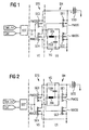
- FIG. 2 shows a further embodiment of the invention Circuit arrangement shown, which is different from the Circuit arrangement according to FIG. 1 only differs in that the delay element VG is not between the input terminal the final stage switching unit ES and the gate connection of the NMOS transistor switching element SE2, but between the input connection of the output stage switching unit ES and the gate terminal of the PMOS transistor switching element SE1 is. This results in the current pulse falling Edge of the first control signal T1 at the input one constructed from a preliminary stage VS and a final stage ES Switching stage STS is generated.
Landscapes
- Engineering & Computer Science (AREA)
- Computer Hardware Design (AREA)
- Physics & Mathematics (AREA)
- Microelectronics & Electronic Packaging (AREA)
- Theoretical Computer Science (AREA)
- General Physics & Mathematics (AREA)
- Computer Networks & Wireless Communication (AREA)
- Nonlinear Science (AREA)
- Computer Security & Cryptography (AREA)
- General Engineering & Computer Science (AREA)
- Semiconductor Integrated Circuits (AREA)
- Electronic Switches (AREA)
- Logic Circuits (AREA)
Abstract
Description
- Figur 1
- eine erste Ausführung einer erfindungsgemäßen Schaltungsanordnung mit einer aus einer Vor- und einer Endstufe gebildeten Schaltstufe,
- Figur 2
- eine zweite Ausführungsform einer erfindungsgemäßen Schaltungsanordnung,
- Figur 3
- eine dritte Ausführungsform der erfindungsgemäßen Schaltungsanordnung mit einer Steuerschaltung zur Auswahl der Schaltflanke des Steuersignals,
- Figur 4
- ein die Schaltung gemäß Figur 3 beschreibendes Signaldiagramm,
- Figur 5
- eine mehrstufige Schaltungsanordnung zur Erzeugung unterschiedlicher Pulsamplituden,
- Figur 6
- ein Beispiel für ein Signaldiagramm zur Beaufschlagung der Eingänge der Schaltung gemäß Figur 5 und
- Figur 7
- das aus dem Signaldiagramm gemäß Figur 6 resultierende Stromprofil als Spannungsabfall über einem Meßwiderstand der Schaltung gemäß Figur 5.
Claims (11)
- Schaltungsanordnung zur Erzeugung von Strompulsen im Versorgungsstrom integrierter Schaltungen mit zumindest einer mit zwei komplementären, zwischen den Versorgungsspannungen (VDD, Masse) der integrierten Schaltung in Serie geschalteten, steuerbaren Schaltelementen (SE1, SE2; SE3, SE4) gebildeten Schalteinheit (SH; VS, ES), deren durch ein erstes Steuersignal (T1) ansteuerbarer Eingangsanschluß mit den Steueranschlüssen der Schaltelemente (SE1, SE2; SE3, SE4) verbunden ist, wobei zwischen dem Eingangsanschluß und entweder dem Steueranschluß des Pull-Up-Schaltelements (SE1, SE3) oder dem Steueranschluß des Pull-Down-Schaltelements (SE2, SE4) ein Verzögerungsglied (VG) angeordnet ist, so daß entweder bei einer steigenden oder einer fallenden Flanke des ersten Steuersignals (T1) ein Strompuls erzeugt wird.
- Schaltungsanordnung nach Anspruch 1, dadurch gekennzeichnet, daß der Schalteinheit (ES) eine weitere Schalteinheit (VS) vorgeschaltet ist, deren Eingangsanschluß direkt mit den Steueranschlüssen der sie bildenden komplementären Schaltelemente (T3, T4) verbunden ist und deren Ausgangsanschluß durch den Verbindungspunkt der beiden komplementären Schaltelemente (T3, T4) gebildet ist, wobei die Serienschaltung dieser Schalteinheiten (VS, ES) eine Schaltstufe (STS) bildet, deren Eingangsanschluß mit dem ersten Steuersignal (T1) ansteuerbar ist.
- Schaltungsanordnung nach Anspruch 1 oder 2, dadurch gekennzeichnet, daß eine Schalteinheit (SH; VS, ES) mit einer CMOS-Inverterschaltung gebildet ist.
- Schaltungsanordnung nach einem der vorhergehenden Ansprüche, dadurch gekennzeichnet, daß mehrere Schalteinheiten (SH) oder Schaltstufen (STS) bezüglich des ersten Steuersignals (T1) parallelgeschaltet sind und das erste Steuersignal (T1) jeweils über eine von einer Steuerschaltung (SST) ansteuerbaren Schaltvorrichtung (SV1, SV2) einer jeweiligen Schalteinheit (SH) oder Schaltstufe (STS) zuführbar ist.
- Schaltungsanordnung nach Anspruch 4, dadurch gekennzeichnet, daß die Schalteinheiten (SH; VS, ES) oder Schaltstufen (STS) derart dimensioniert sind, daß sie unterschiedlich hohe Strompulse erzeugen.
- Schaltungsanordnung nach einem der Ansprüche 4 oder 5, dadurch gekennzeichnet, daß die Schalteinheiten (SH; VS, ES) oder Schaltstufen (STS) derart gebildet sind, daß die Strompulse bei einer steigenden Flanke des ersten Steuersignals (T1) erzeugt werden.
- Schaltungsanordnung nach einem der Ansprüche 4 oder 5, dadurch gekennzeichnet, daß die Schalteinheiten (SH; VS, ES) oder Schaltstufen (STS) derart gebildet sind, daß die Strompulse bei einer fallenden Flanke des ersten Steuersignals (T1) erzeugt werden.
- Schaltungsanordnung nach einem der Ansprüche 4 oder 5, dadurch gekennzeichnet, daß die Schalteinheiten (SH; VS, ES) oder Schaltstufen (STS) einer ersten Gruppe derart gebildet sind, daß die Strompulse bei einer steigenden Flanke des ersten Steuersignals (T1) erzeugt werden und die Schalteinheiten (SH; VS, ES) oder Schaltstufen (STS) einer zweiten Gruppe derart gebildet sind, daß die Strompulse bei einer fallenden Flanke des ersten Steuersignals (T1) erzeugt werden.
- Schaltungsanordnung nach einem der Ansprüche 1 bis 3, dadurch gekennzeichnet, daß eine erste Anzahl von Schalteinheiten (SH; VS, ES) oder Schaltstufen (STS) bezüglich des ersten Steuersignals (T1) parallelgeschaltet sind und eine Gruppe bilden und das erste Steuersignal (T1) jeweils über eine von einer Steuerschaltung (SST) ansteuerbaren Schaltvorrichtung (SV1) einer jeweiligen Schalteinheit (SH) oder Schaltstufe (STS) der Gruppe zuführbar ist, wobei die Schalteinheiten (SH; VS, ES) oder Schaltstufen (STS) der Gruppe derart gebildet sind, daß die Strompulse bei einer steigenden Flanke des ersten Steuersignals (T1) erzeugt werden,
und daß eine zweite Anzahl von Schalteinheiten (SH) oder Schaltstufen (STS) bezüglich eines zweiten, zum ersten Steuersignal (T1) komplementären Steuersignals (T2) parallelgeschaltet sind und eine weitere Gruppe bilden und das zweite Steuersignal (T2) jeweils über eine von der Steuerschaltung (SST) ansteuerbaren Schaltvorrichtung (SV2) einer jeweiligen Schalteinheit (SH) oder Schaltstufe (STS) der weiteren Gruppe zuführbar ist, wobei die Schalteinheiten (SH) oder Schaltstufen (STS) der weiteren Gruppe derart gebildet sind, daß die Strompulse bei einer steigenden Flanke des zweiten Steuersignal (T2) bzw. einer fallenden Flanke des ersten Steuersignals (T1) erzeugt werden. - Schaltungsanordnung nach einem der Ansprüche 4 bis 9, dadurch gekennzeichnet, daß die Steuerschaltung (SST) einen Signalgenerator (SG) zur Erzeugung von Bitmustern zur Ansteuerung der Schaltvorrichtungen (SV1, SV2) aufweist.
- Schaltungsanordnung nach Anspruch 10, dadurch gekennzeichnet, daß der Signalgenerator (SG) ein Zufallszahlengenerator ist.
Priority Applications (1)
| Application Number | Priority Date | Filing Date | Title |
|---|---|---|---|
| EP00931090A EP1177628B1 (de) | 1999-05-12 | 2000-04-28 | Schaltungsanordnung zur erzeugung von strompulsen im versorgungsstrom integrierter schaltungen |
Applications Claiming Priority (4)
| Application Number | Priority Date | Filing Date | Title |
|---|---|---|---|
| EP99109552 | 1999-05-12 | ||
| EP99109552 | 1999-05-12 | ||
| EP00931090A EP1177628B1 (de) | 1999-05-12 | 2000-04-28 | Schaltungsanordnung zur erzeugung von strompulsen im versorgungsstrom integrierter schaltungen |
| PCT/EP2000/003879 WO2000070761A1 (de) | 1999-05-12 | 2000-04-28 | Schaltungsanordnung zur erzeugung von strompulsen im versorgungsstrom integrierter schaltungen |
Publications (2)
| Publication Number | Publication Date |
|---|---|
| EP1177628A1 EP1177628A1 (de) | 2002-02-06 |
| EP1177628B1 true EP1177628B1 (de) | 2003-08-06 |
Family
ID=8238172
Family Applications (1)
| Application Number | Title | Priority Date | Filing Date |
|---|---|---|---|
| EP00931090A Expired - Lifetime EP1177628B1 (de) | 1999-05-12 | 2000-04-28 | Schaltungsanordnung zur erzeugung von strompulsen im versorgungsstrom integrierter schaltungen |
Country Status (7)
| Country | Link |
|---|---|
| US (1) | US7017048B2 (de) |
| EP (1) | EP1177628B1 (de) |
| JP (1) | JP2003500881A (de) |
| CN (1) | CN1175570C (de) |
| DE (1) | DE50003195D1 (de) |
| ES (1) | ES2204603T3 (de) |
| WO (1) | WO2000070761A1 (de) |
Families Citing this family (20)
| Publication number | Priority date | Publication date | Assignee | Title |
|---|---|---|---|---|
| FR2811790A1 (fr) * | 2000-07-11 | 2002-01-18 | Schlumberger Systems & Service | Microcontroleur securise contre des attaques dites en courant |
| DE10162309A1 (de) * | 2001-12-19 | 2003-07-03 | Philips Intellectual Property | Verfahren und Anordnung zur Erhöhung der Sicherheit von Schaltkreisen gegen unbefugten Zugriff |
| DE10227618B4 (de) | 2002-06-20 | 2007-02-01 | Infineon Technologies Ag | Logikschaltung |
| US7187227B2 (en) * | 2002-08-07 | 2007-03-06 | Nippon Telegraph And Telephone Corporation | Driver circuit |
| KR100528464B1 (ko) * | 2003-02-06 | 2005-11-15 | 삼성전자주식회사 | 스마트카드의 보안장치 |
| US20040265499A1 (en) * | 2003-06-24 | 2004-12-30 | Nokia Corporation | Method of forming patterns on articles |
| KR100706787B1 (ko) * | 2004-11-29 | 2007-04-11 | 삼성전자주식회사 | 향상된 보안 기능을 갖는 스마트 카드 |
| CN100337399C (zh) * | 2004-12-14 | 2007-09-12 | 重庆大学 | 具有上升沿提升能力的电流脉冲下降沿线性可调的控制方法及装置 |
| EP1831812A1 (de) | 2004-12-20 | 2007-09-12 | Philips Intellectual Property & Standards GmbH | Datenverarbeitungsvorrichtung und verfahren für den betrieb einer derartigen datenverarbeitungsvorrichtung |
| JP4641215B2 (ja) * | 2005-05-20 | 2011-03-02 | 株式会社日立製作所 | 負荷駆動回路、集積回路、及びプラズマディスプレイ |
| EP2235874A1 (de) * | 2007-12-13 | 2010-10-06 | Nxp B.V. | Elektronische schaltung und verfahren zur maskierung von stromanforderungen einer elektronischen schaltung |
| CN101860351B (zh) * | 2009-04-09 | 2012-12-12 | 智原科技股份有限公司 | 脉冲干扰消除电路 |
| CN102025347B (zh) * | 2009-09-21 | 2013-06-19 | 联咏科技股份有限公司 | 开关装置及其控制信号产生器 |
| US8334705B1 (en) | 2011-10-27 | 2012-12-18 | Certicom Corp. | Analog circuitry to conceal activity of logic circuitry |
| US8635467B2 (en) | 2011-10-27 | 2014-01-21 | Certicom Corp. | Integrated circuit with logic circuitry and multiple concealing circuits |
| WO2015089346A1 (en) | 2013-12-13 | 2015-06-18 | Battelle Memorial Institute | Electronic component classification |
| DE102014009808A1 (de) | 2014-07-03 | 2016-01-07 | Andreas Gornik | Hardware Schutzmaßnahme zur Erschwerung von Seitenkanalattacken |
| FR3061580A1 (fr) * | 2017-01-03 | 2018-07-06 | Stmicroelectronics (Rousset) Sas | Procede et dispositif de gestion de la consommation en courant d'un module integre. |
| US10789550B2 (en) | 2017-04-13 | 2020-09-29 | Battelle Memorial Institute | System and method for generating test vectors |
| US10630272B1 (en) * | 2019-04-08 | 2020-04-21 | Kandou Labs, S.A. | Measurement and correction of multiphase clock duty cycle and skew |
Family Cites Families (7)
| Publication number | Priority date | Publication date | Assignee | Title |
|---|---|---|---|---|
| US4829199A (en) | 1987-07-13 | 1989-05-09 | Ncr Corporation | Driver circuit providing load and time adaptive current |
| US4797579A (en) * | 1987-07-27 | 1989-01-10 | Raytheon Company | CMOS VLSI output driver with controlled rise and fall times |
| US5041741A (en) * | 1990-09-14 | 1991-08-20 | Ncr Corporation | Transient immune input buffer |
| JPH05145032A (ja) * | 1991-11-25 | 1993-06-11 | Toshiba Corp | 入力回路 |
| US5598348A (en) * | 1994-09-22 | 1997-01-28 | Sun Microsystems, Inc. | Method and apparatus for analyzing the power network of a VLSI circuit |
| US5625803A (en) * | 1994-12-14 | 1997-04-29 | Vlsi Technology, Inc. | Slew rate based power usage simulation and method |
| US5768145A (en) | 1996-06-11 | 1998-06-16 | Lsi Logic Corporation | Parametrized waveform processor for gate-level power analysis tool |
-
2000
- 2000-04-28 JP JP2000619102A patent/JP2003500881A/ja not_active Withdrawn
- 2000-04-28 DE DE50003195T patent/DE50003195D1/de not_active Expired - Lifetime
- 2000-04-28 EP EP00931090A patent/EP1177628B1/de not_active Expired - Lifetime
- 2000-04-28 WO PCT/EP2000/003879 patent/WO2000070761A1/de not_active Ceased
- 2000-04-28 CN CNB008102562A patent/CN1175570C/zh not_active Expired - Fee Related
- 2000-04-28 ES ES00931090T patent/ES2204603T3/es not_active Expired - Lifetime
-
2001
- 2001-11-13 US US10/021,689 patent/US7017048B2/en not_active Expired - Fee Related
Also Published As
| Publication number | Publication date |
|---|---|
| CN1175570C (zh) | 2004-11-10 |
| US20020067198A1 (en) | 2002-06-06 |
| WO2000070761A1 (de) | 2000-11-23 |
| US7017048B2 (en) | 2006-03-21 |
| DE50003195D1 (de) | 2003-09-11 |
| CN1360757A (zh) | 2002-07-24 |
| ES2204603T3 (es) | 2004-05-01 |
| JP2003500881A (ja) | 2003-01-07 |
| EP1177628A1 (de) | 2002-02-06 |
Similar Documents
| Publication | Publication Date | Title |
|---|---|---|
| EP1177628A1 (de) | Schaltungsanordnung zur erzeugung von strompulsen im versorgungsstrom integrierter schaltungen | |
| DE10324875B4 (de) | Störimpuls-Detektionsschaltung und intelligente Karte | |
| DE19531962C2 (de) | Taktsignalverteilerschaltung | |
| DE10141939B4 (de) | Flip-Flop-Schaltung zur taktsignalabhängigen Datenpufferung und diese enthaltender Signalhöhenkomparator | |
| DE4326134B4 (de) | Eingangswechseldetektorschaltung | |
| DE602004004533T2 (de) | Phasenmischschaltung mit verzögertem regelkreis | |
| DE102008006301B4 (de) | Schaltungsanordnung zum Detektieren von Spannungsänderungen und Verfahren zum Detektieren einer Spannungsänderung | |
| DE68927552T2 (de) | Speichervorrichtungen | |
| DE112016006170T5 (de) | Puf-werterzeugung unter verwendung einer anti-schmelzsicherungs-speicheranordnung | |
| DE69327612T2 (de) | Schaltung und Verfahren zur Generierung eines stabilen Taktsignals mit Frequenzvervielfachung | |
| DE3930932A1 (de) | Ausgangsrueckkopplungssteuerschaltung fuer integrierte schaltung | |
| DE102016118534A1 (de) | Schaltung und Verfahren zum Prüfen der Integrität eines Steuersignals | |
| DE10103307B4 (de) | Integrierte Halbleiterschaltung und Verfahren zu deren Initialisierung | |
| DE10130123B4 (de) | Verzögerungsregelkreis zur Erzeugung komplementärer Taktsignale | |
| DE60124194T2 (de) | Verriegelungsschaltung und D-Flipflop | |
| DE4318422A1 (de) | Integrierte Schaltung mit Registerstufen | |
| DE69426477T2 (de) | Impulssignalfilterschaltung und integrierte Schaltung zur Herstellung einer solchen Schaltung | |
| DE69030575T2 (de) | Integrierte Halbleiterschaltung mit einem Detektor | |
| DE19709229A1 (de) | Ein Zeitablauf-konsistenter dynamischer Vergleich mit einer Zwangsfehlgriffschaltung | |
| DE19644443C2 (de) | Adressübergangs-Detektorschaltung | |
| DE68912794T2 (de) | Integrierte Halbleiterschaltung. | |
| DE69417949T2 (de) | Adressenübergangsabfühlschaltung und Steuerungsverfahren | |
| EP0824789B1 (de) | Vorrichtung zur takterzeugung für cmos-schaltungen mit dynamischen registern | |
| DE19742702B4 (de) | Adressübergangs-Detektionsschaltung | |
| DE3887817T2 (de) | Steuerschaltung für Leseverstärker. |
Legal Events
| Date | Code | Title | Description |
|---|---|---|---|
| PUAI | Public reference made under article 153(3) epc to a published international application that has entered the european phase |
Free format text: ORIGINAL CODE: 0009012 |
|
| 17P | Request for examination filed |
Effective date: 20011109 |
|
| AK | Designated contracting states |
Kind code of ref document: A1 Designated state(s): AT BE CH CY DE DK ES FI FR GB GR IE IT LI LU MC NL PT SE |
|
| AX | Request for extension of the european patent |
Free format text: AL;LT;LV;MK;RO;SI |
|
| GRAH | Despatch of communication of intention to grant a patent |
Free format text: ORIGINAL CODE: EPIDOS IGRA |
|
| GRAH | Despatch of communication of intention to grant a patent |
Free format text: ORIGINAL CODE: EPIDOS IGRA |
|
| GRAA | (expected) grant |
Free format text: ORIGINAL CODE: 0009210 |
|
| AK | Designated contracting states |
Designated state(s): DE ES FR GB IT |
|
| REG | Reference to a national code |
Ref country code: GB Ref legal event code: FG4D Free format text: NOT ENGLISH |
|
| REG | Reference to a national code |
Ref country code: IE Ref legal event code: FG4D Free format text: GERMAN |
|
| REF | Corresponds to: |
Ref document number: 50003195 Country of ref document: DE Date of ref document: 20030911 Kind code of ref document: P |
|
| GBT | Gb: translation of ep patent filed (gb section 77(6)(a)/1977) | ||
| LTIE | Lt: invalidation of european patent or patent extension |
Effective date: 20030806 |
|
| REG | Reference to a national code |
Ref country code: IE Ref legal event code: FD4D |
|
| PGFP | Annual fee paid to national office [announced via postgrant information from national office to epo] |
Ref country code: ES Payment date: 20040423 Year of fee payment: 5 |
|
| REG | Reference to a national code |
Ref country code: ES Ref legal event code: FG2A Ref document number: 2204603 Country of ref document: ES Kind code of ref document: T3 |
|
| ET | Fr: translation filed | ||
| PLBE | No opposition filed within time limit |
Free format text: ORIGINAL CODE: 0009261 |
|
| STAA | Information on the status of an ep patent application or granted ep patent |
Free format text: STATUS: NO OPPOSITION FILED WITHIN TIME LIMIT |
|
| 26N | No opposition filed |
Effective date: 20040507 |
|
| PG25 | Lapsed in a contracting state [announced via postgrant information from national office to epo] |
Ref country code: IT Free format text: LAPSE BECAUSE OF NON-PAYMENT OF DUE FEES Effective date: 20050428 |
|
| PG25 | Lapsed in a contracting state [announced via postgrant information from national office to epo] |
Ref country code: ES Free format text: LAPSE BECAUSE OF NON-PAYMENT OF DUE FEES Effective date: 20050429 |
|
| REG | Reference to a national code |
Ref country code: ES Ref legal event code: FD2A Effective date: 20050429 |
|
| REG | Reference to a national code |
Ref country code: FR Ref legal event code: PLFP Year of fee payment: 17 |
|
| REG | Reference to a national code |
Ref country code: FR Ref legal event code: PLFP Year of fee payment: 18 |
|
| PGFP | Annual fee paid to national office [announced via postgrant information from national office to epo] |
Ref country code: FR Payment date: 20170419 Year of fee payment: 18 Ref country code: GB Payment date: 20170419 Year of fee payment: 18 Ref country code: DE Payment date: 20170613 Year of fee payment: 18 |
|
| REG | Reference to a national code |
Ref country code: DE Ref legal event code: R119 Ref document number: 50003195 Country of ref document: DE |
|
| GBPC | Gb: european patent ceased through non-payment of renewal fee |
Effective date: 20180428 |
|
| PG25 | Lapsed in a contracting state [announced via postgrant information from national office to epo] |
Ref country code: DE Free format text: LAPSE BECAUSE OF NON-PAYMENT OF DUE FEES Effective date: 20181101 |
|
| PG25 | Lapsed in a contracting state [announced via postgrant information from national office to epo] |
Ref country code: GB Free format text: LAPSE BECAUSE OF NON-PAYMENT OF DUE FEES Effective date: 20180428 |
|
| PG25 | Lapsed in a contracting state [announced via postgrant information from national office to epo] |
Ref country code: FR Free format text: LAPSE BECAUSE OF NON-PAYMENT OF DUE FEES Effective date: 20180430 |