EP1175090B1 - Signal transfer circuitry with offset correction - Google Patents
Signal transfer circuitry with offset correction Download PDFInfo
- Publication number
- EP1175090B1 EP1175090B1 EP01117841A EP01117841A EP1175090B1 EP 1175090 B1 EP1175090 B1 EP 1175090B1 EP 01117841 A EP01117841 A EP 01117841A EP 01117841 A EP01117841 A EP 01117841A EP 1175090 B1 EP1175090 B1 EP 1175090B1
- Authority
- EP
- European Patent Office
- Prior art keywords
- signal
- removal
- circuit
- photoelements
- photoelement
- Prior art date
- Legal status (The legal status is an assumption and is not a legal conclusion. Google has not performed a legal analysis and makes no representation as to the accuracy of the status listed.)
- Expired - Lifetime
Links
- 238000012546 transfer Methods 0.000 title description 98
- 238000012937 correction Methods 0.000 title description 25
- 238000000034 method Methods 0.000 claims description 9
- 230000010354 integration Effects 0.000 description 28
- 239000003990 capacitor Substances 0.000 description 26
- 238000003384 imaging method Methods 0.000 description 18
- 238000012545 processing Methods 0.000 description 18
- 238000010586 diagram Methods 0.000 description 16
- 238000005286 illumination Methods 0.000 description 12
- 238000012360 testing method Methods 0.000 description 11
- 102100035474 DNA polymerase kappa Human genes 0.000 description 9
- 101710108091 DNA polymerase kappa Proteins 0.000 description 9
- HBGGXOJOCNVPFY-UHFFFAOYSA-N diisononyl phthalate Chemical compound CC(C)CCCCCCOC(=O)C1=CC=CC=C1C(=O)OCCCCCCC(C)C HBGGXOJOCNVPFY-UHFFFAOYSA-N 0.000 description 9
- 230000000694 effects Effects 0.000 description 7
- 238000002310 reflectometry Methods 0.000 description 7
- 239000000758 substrate Substances 0.000 description 7
- 238000004519 manufacturing process Methods 0.000 description 6
- 230000003287 optical effect Effects 0.000 description 6
- 230000008569 process Effects 0.000 description 6
- 239000000835 fiber Substances 0.000 description 5
- 230000006870 function Effects 0.000 description 5
- 230000003321 amplification Effects 0.000 description 4
- 230000008901 benefit Effects 0.000 description 4
- 230000007850 degeneration Effects 0.000 description 4
- 238000003199 nucleic acid amplification method Methods 0.000 description 4
- 238000012935 Averaging Methods 0.000 description 3
- 230000002411 adverse Effects 0.000 description 3
- 238000013459 approach Methods 0.000 description 3
- 238000001914 filtration Methods 0.000 description 3
- 238000002347 injection Methods 0.000 description 3
- 239000007924 injection Substances 0.000 description 3
- 230000003071 parasitic effect Effects 0.000 description 3
- 230000000737 periodic effect Effects 0.000 description 3
- 230000035945 sensitivity Effects 0.000 description 3
- 238000013519 translation Methods 0.000 description 3
- 230000001419 dependent effect Effects 0.000 description 2
- 230000007246 mechanism Effects 0.000 description 2
- 230000004044 response Effects 0.000 description 2
- 230000002441 reversible effect Effects 0.000 description 2
- 238000005070 sampling Methods 0.000 description 2
- 101100384801 Bos taurus CGN1 gene Proteins 0.000 description 1
- 229910019543 CoxW Inorganic materials 0.000 description 1
- 241001522296 Erithacus rubecula Species 0.000 description 1
- XUIMIQQOPSSXEZ-UHFFFAOYSA-N Silicon Chemical compound [Si] XUIMIQQOPSSXEZ-UHFFFAOYSA-N 0.000 description 1
- 238000004458 analytical method Methods 0.000 description 1
- 230000003466 anti-cipated effect Effects 0.000 description 1
- 238000003491 array Methods 0.000 description 1
- 238000012512 characterization method Methods 0.000 description 1
- 238000005314 correlation function Methods 0.000 description 1
- 230000003111 delayed effect Effects 0.000 description 1
- 238000013461 design Methods 0.000 description 1
- 238000007599 discharging Methods 0.000 description 1
- 238000011143 downstream manufacturing Methods 0.000 description 1
- 238000005516 engineering process Methods 0.000 description 1
- 239000005357 flat glass Substances 0.000 description 1
- 230000007274 generation of a signal involved in cell-cell signaling Effects 0.000 description 1
- 238000002955 isolation Methods 0.000 description 1
- 238000013507 mapping Methods 0.000 description 1
- 238000012986 modification Methods 0.000 description 1
- 230000004048 modification Effects 0.000 description 1
- 108091008695 photoreceptors Proteins 0.000 description 1
- 230000009467 reduction Effects 0.000 description 1
- 229910052710 silicon Inorganic materials 0.000 description 1
- 239000010703 silicon Substances 0.000 description 1
- 238000004088 simulation Methods 0.000 description 1
Images


Classifications
-
- H—ELECTRICITY
- H03—ELECTRONIC CIRCUITRY
- H03F—AMPLIFIERS
- H03F3/00—Amplifiers with only discharge tubes or only semiconductor devices as amplifying elements
- H03F3/45—Differential amplifiers
- H03F3/45071—Differential amplifiers with semiconductor devices only
- H03F3/45076—Differential amplifiers with semiconductor devices only characterised by the way of implementation of the active amplifying circuit in the differential amplifier
- H03F3/45475—Differential amplifiers with semiconductor devices only characterised by the way of implementation of the active amplifying circuit in the differential amplifier using IC blocks as the active amplifying circuit
-
- H—ELECTRICITY
- H03—ELECTRONIC CIRCUITRY
- H03F—AMPLIFIERS
- H03F1/00—Details of amplifiers with only discharge tubes, only semiconductor devices or only unspecified devices as amplifying elements
- H03F1/30—Modifications of amplifiers to reduce influence of variations of temperature or supply voltage or other physical parameters
- H03F1/303—Modifications of amplifiers to reduce influence of variations of temperature or supply voltage or other physical parameters using a switching device
-
- H—ELECTRICITY
- H03—ELECTRONIC CIRCUITRY
- H03F—AMPLIFIERS
- H03F3/00—Amplifiers with only discharge tubes or only semiconductor devices as amplifying elements
- H03F3/04—Amplifiers with only discharge tubes or only semiconductor devices as amplifying elements with semiconductor devices only
- H03F3/08—Amplifiers with only discharge tubes or only semiconductor devices as amplifying elements with semiconductor devices only controlled by light
- H03F3/087—Amplifiers with only discharge tubes or only semiconductor devices as amplifying elements with semiconductor devices only controlled by light with IC amplifier blocks
-
- H—ELECTRICITY
- H04—ELECTRIC COMMUNICATION TECHNIQUE
- H04N—PICTORIAL COMMUNICATION, e.g. TELEVISION
- H04N25/00—Circuitry of solid-state image sensors [SSIS]; Control thereof
- H04N25/60—Noise processing, e.g. detecting, correcting, reducing or removing noise
- H04N25/67—Noise processing, e.g. detecting, correcting, reducing or removing noise applied to fixed-pattern noise, e.g. non-uniformity of response
- H04N25/671—Noise processing, e.g. detecting, correcting, reducing or removing noise applied to fixed-pattern noise, e.g. non-uniformity of response for non-uniformity detection or correction
- H04N25/677—Noise processing, e.g. detecting, correcting, reducing or removing noise applied to fixed-pattern noise, e.g. non-uniformity of response for non-uniformity detection or correction for reducing the column or line fixed pattern noise
-
- H—ELECTRICITY
- H04—ELECTRIC COMMUNICATION TECHNIQUE
- H04N—PICTORIAL COMMUNICATION, e.g. TELEVISION
- H04N25/00—Circuitry of solid-state image sensors [SSIS]; Control thereof
- H04N25/70—SSIS architectures; Circuits associated therewith
- H04N25/701—Line sensors
-
- H—ELECTRICITY
- H04—ELECTRIC COMMUNICATION TECHNIQUE
- H04N—PICTORIAL COMMUNICATION, e.g. TELEVISION
- H04N25/00—Circuitry of solid-state image sensors [SSIS]; Control thereof
- H04N25/70—SSIS architectures; Circuits associated therewith
- H04N25/76—Addressed sensors, e.g. MOS or CMOS sensors
- H04N25/767—Horizontal readout lines, multiplexers or registers
-
- H—ELECTRICITY
- H04—ELECTRIC COMMUNICATION TECHNIQUE
- H04N—PICTORIAL COMMUNICATION, e.g. TELEVISION
- H04N25/00—Circuitry of solid-state image sensors [SSIS]; Control thereof
- H04N25/70—SSIS architectures; Circuits associated therewith
- H04N25/76—Addressed sensors, e.g. MOS or CMOS sensors
- H04N25/77—Pixel circuitry, e.g. memories, A/D converters, pixel amplifiers, shared circuits or shared components
-
- H—ELECTRICITY
- H04—ELECTRIC COMMUNICATION TECHNIQUE
- H04N—PICTORIAL COMMUNICATION, e.g. TELEVISION
- H04N25/00—Circuitry of solid-state image sensors [SSIS]; Control thereof
- H04N25/70—SSIS architectures; Circuits associated therewith
- H04N25/76—Addressed sensors, e.g. MOS or CMOS sensors
- H04N25/78—Readout circuits for addressed sensors, e.g. output amplifiers or A/D converters
-
- H—ELECTRICITY
- H03—ELECTRONIC CIRCUITRY
- H03F—AMPLIFIERS
- H03F2200/00—Indexing scheme relating to amplifiers
- H03F2200/249—A switch coupled in the input circuit of an amplifier being controlled by a circuit, e.g. feedback circuitry being controlling the switch
-
- H—ELECTRICITY
- H03—ELECTRONIC CIRCUITRY
- H03F—AMPLIFIERS
- H03F2203/00—Indexing scheme relating to amplifiers with only discharge tubes or only semiconductor devices as amplifying elements covered by H03F3/00
- H03F2203/45—Indexing scheme relating to differential amplifiers
- H03F2203/45212—Indexing scheme relating to differential amplifiers the differential amplifier being designed to have a reduced offset
Definitions
- the present invention relates generally to signal transfer circuitry and more particularly to circuitry for transferring individual signals from an array of photoreceivers to computational circuitry.
- An accurate determination of the path of a device across a surface is important in a variety of applications. For example, if a faithful representation of an image of a scanned original is to be acquired, there must be accurate information as to the travel of the scanning device along the original.
- the captured image provided by a scanner is a pixel data array that is stored in memory in a digital format.
- a distortion-free image requires a faithful mapping of the original image to the pixel data array.
- the patent to Ertel et al. describes use of an optical sensor array to collect some form of "signature" of an original.
- the signature may be provided by illuminating and imaging the surface texture or other optical characteristics of the original.
- the light intensity will vary on a pixel-by-pixel basis with variations in surface texture.
- JP-A-5,219,440 discloses circuitry for transferring signals which comprises plural signal generating circuits, each of which has an output; and plural DC removal means for removing spatial frequency components from the outputs, each of the DC removal means being operatively associated with a particular circuit and having a primary input connected to receive a signal of interest from the output of the particular circuit, each DC removal means including at least one secondary input connected to receive a signal output from one of the circuits proximal the particular circuit, of each DC removal means including difference means for providing an output signal responsive to analog signal differences between the signal of interest and the signal outputs received at the at least one secondary input.
- U.S. Pat. No. 4,409,483 to Turley describes an apparatus in which sensors (pixels) are paired and the sensor pairs are connected to a differential amplifier for determining the difference of the output signals from the two sensors.
- the apparatus overcomes the problem of storing and transferring large signals from the sensors by transferring the difference signals only.
- a critical element of the design of a system such as the one described by Ertel et al. is the circuitry which maintains the signal-to-noise ratio of each photoelement at a sufficiently high level to reliably determine the signature of the original. If the signal is the difference in reflectivity from pixel to pixel as a result of slight variations in paper texture of a white paper, the variations in reflectivity may be approximately six percent. If the sample rate objectives and the amount of possible subsequent signal averaging are considered, then noise terms in the signal must be less than the six percent paper reflectivity variation signal if useful information is to be obtained.
- noise is one concern in the processing of signals from photoelements in a photoreceiver array.
- Another concern is manufacturing-induced variations in the performance of processing circuitry. Operations that rely upon computations of the differences in reflectivity from one pixel to another pixel are susceptible to error if electrically parallel transfer circuits vary in performance. In the ideal, there are no pixel-to-pixel signal differences due to variations in signal transfer circuit performance, so that differences between pixel signals are solely attributable to differences in light reception at the photoelements.
- circuit devices vary in performance, even when the devices are formed by the same fabrication process.
- illumination optics may create consistent neighbourhood-to-neighbourhood variations in the illumination of the surface to be imaged. Non-uniform illumination will cause artifacts.
- a consistent localized pattern is one in which a portion of the photoelement array is directed at a surface area having a dark background, while the remainder of the photoelements are directed at an unshaded area of the surface.
- Circuitry and a method for transferring signals from a photoelement array to computational circuits include parallel transfer amplifiers that receive periodic offset correction to reduce the susceptability of signal processing to differences in performance among the transfer amplifiers.
- the circuitry for transferring signals includes spatial frequency band filtering amplifiers to suppress the effects of such artifacts as multi-photoelement patterns of light reception at the photoelement array.
- DC removal will be used as a shorthand term to denote spatial frequency band filtering. It is to be understood that the term “DC removal,” as used herein, encompasses not only the removal of DC spatial components, but also the removal of spatial frequency components at either or both low and high frequencies.
- each transfer amplifier when in a readout mode, each transfer amplifier has a first input that is connected to receive a signal indicative of light received at a photoelement.
- the photoelements in the array may be arranged in columns and rows, with the photoelements in a particular column being sequentially connected to the first input of a particular transfer amplifier, but this is not critical.
- Each transfer amplifier has a second input connected to a source of a reference voltage (e.g., 1.75 volts).
- the transfer amplifiers operate as differential circuits, so that an output is responsive to the difference between the voltage states at the first and second inputs. However, during a reset interval between readout intervals, both of the first and second inputs are connected' to the source of the reference voltage.
- the output of a transfer amplifier is momentarily connected to a source of a reset voltage (e.g., 3.25 volts).
- An offset reduction circuit is provided to generate an offset adjustment signal in response to detecting a voltage difference between the reset voltage and the voltage state at the output after the output has been disconnected from the source of the reset voltage. In this manner, the adjustment signal may be applied to the transfer amplifier of interest to reduce or eliminate any difference in performance between the transfer amplifier and other transfer amplifiers.
- each transfer amplifier preferably includes a sample-and-hold arrangement to store the offset adjustment signal, so that each transfer amplifier only needs to be periodically refreshed.
- a timing sequence is provided to achieve periodic refreshes without lengthening intervals between photoelement signal readouts.
- each transfer amplifier includes the sample-and-hold arrangement, the transfer amplifiers have three modes of operation.
- a readout mode the second input is connected to the source of the reference voltage, while the first input is connected to a photoelement.
- the amplifier output voltage is in turn supplied to downstream processing circuitry.
- the internal sample-and-hold arrangement will provide offset correction.
- a second mode of operation is a passive reset mode.
- the reset is "passive" because the offset adjustment signal is not updated.
- the passive reset mode may be of poor quality until the first active offset adjustment operation has been executed.
- the two inputs of the transfer amplifier are connected together and the output remains connected to the source of the reset voltage.
- the third mode of operation is the active reset mode.
- the two inputs of a transfer amplifier are connected to the source of the reference voltage. However, the output is only momentarily connected to the source of the reset voltage. Once disconnected, the output is connected to the offset adjustment circuit, which determines the appropriate offset adjustment signal to be stored by the sample-and-hold arrangement until the next active reset operation.
- each transfer amplifier alternates between the readout mode and the passive reset mode.
- the 1/f offset drift components are sufficiently slow, so that an update after each eighth readout of the photoelement array is an adequate rate.
- the invention includes DC removal amplifiers to suppress multi-photoelement light patterns and other artifacts.
- the DC removal amplifiers remove spatial frequency components at both low and high frequencies from the outputs of the transfer amplifiers.
- Each DC removal amplifier includes a primary input that is connected to receive a signal of interest from a particular photoelement.
- Each DC removal amplifier also includes at least one secondary input connected to receive an output signal from a photoelement proximal to the particular photoelement. In effect, an averaging of the secondary inputs occurs and the resulting average value is subtracted from the primary input.
- the DC removal amplifiers in addition to removing low spatial frequency components, also have an inherent low-pass characteristic at a frequency corresponding to twice the pixel spacing.
- the DC removal amplifiers inherently have a band-pass characteristic.
- the inherent low-pass element of the band-pass characteristic may be modified by multiplying the secondary inputs by different weighting factors prior to the averaging.
- the weighting factors can be positive or negative numbers.
- the DC removal amplifier may be formed of first and second differential cells, with the second differential cell having a negative feedback loop from its output to its input.
- the second differential cell may also have a DC input to establish a mid range voltage that facilitates downstream differential operations.
- the DC removal amplifier may include offset correction and may include a switching network that enables a user to switch inputs to the DC removal amplifier or to set the operation of the amplifier in a test mode.
- a portable, hand-held scanning device 10 is shown as having followed a meandering path 12 along an original 14.
- the original may be a piece of paper, but the invention may be used with other imaging-bearing substrates.
- the positions of inherent structural features, such as paper fibers may be tracked and the resulting positional information may be used to rectify image data.
- the invention may be used in other applications.
- the scanning device 10 is preferably self-contained and battery operated. However, the device may include a connection to an external source of power or to data ports of computers or networks.
- the scanning device includes an image display 16. The display may provide almost immediate viewing of a captured image. The display is not critical.
- the scanning device 10 allows three degrees of freedom, with two being in translation and one in rotation.
- the first degree is the side-to-side movement (X axis movement) along the original 14.
- the second degree of freedom is movement upwardly and downwardly along the original (Y axis movement).
- the third degree of freedom is the ability to operate the device with rotational misalignment of a linear array of image sensor elements relative to the edge of the original 14 ( ⁇ -misalignment as a result of Z axis movement). That is, it is not necessary to maintain the linear array of imaging elements perpendicular to the direction of device translation.
- the bottom side 18 of the scanning device 10 includes a pivoting member 20 that aids in maintaining proper contact between the original 14 and an imaging sensor 22.
- Navigation sensors 24 and 26 are located at the opposed ends of the imaging sensor. Because the navigation sensors are mounted on the pivoting member, the navigation sensors are in a fixed location relative to the imaging sensor.
- the imaging sensor 22 is preferably a contact image device, but for applications in which compactness is less of a concern or a smaller image is desired, sensors employing projection optics may be employed, with magnification less than unity.
- Contact imaging devices typically employ lenses sold under the trademark SELFOC, which is a federally-registered mark of Nippon Sheet Glass Company Limited. Less conventionally, contact imaging can be obtained using interleaved array elements of sources and proximal sensors, without any imaging lenses. Conventional imaging sensors for scanning applications may be used.
- the imaging sensor may be part of a unit that also includes an illumination source, illumination optics, and image transfer optics.
- the meandering path 12 is shown as having four and a fraction swaths, i.e., side-to-side passes across the original 14.
- a useful imaging sensor 22 for most applications has a length within the range of 25 mm and 100 mm.
- the swaths should include regions of overlap, so that a stitching process may be used to produce a faithful representation of the scanned original.
- the scanning device 10 includes at least one navigation sensor 24 or 26.
- the device includes a pair of navigation sensors, with the sensors being at opposite ends of the imaging sensor 22. While one-dimensional arrays of photoelements that are mounted orthogonally to each other may be used, the much preferred embodiment is one in which each navigation sensor is a two-dimensional array of elements.
- the navigation sensors 24 and 26 are used to track movement of the scanning device 10 relative to the original.
- Each navigation sensor is an array of photoelements that is formed on an integrated circuit substrate that includes readout and signal processing circuitry.
- the position accuracy necessary over the range of a pixel distance of 40 ⁇ m is 2.0 ⁇ m.
- the very high positional accuracy requires individual photoelements that are no larger than tens of microns in length in order to acquire sufficiently differing signals from element to element.
- the pixel size desired on the paper original 14 is 40 ⁇ m and a magnification of 1.5 is achieved by the imaging optics, so that the photoreceptor elements of the navigation sensors 24 and 26 are 60 ⁇ m ⁇ 60 ⁇ m. A greater optical magnification would enable larger pixels to be used.
- Each navigation sensor may be an array having sixty-four columns and thirty-two rows. However, none of these numbers is critical to the invention.
- the desired signal is the difference in reflectivity from pixel to pixel, as caused by variations along the surface of the original 14.
- the reflectivity may vary by only approximately six percent of the basic reflectivity of the white paper. Consequently, the circuitry to be described below must be designed to minimize noise and to ensure voltage stability.
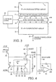
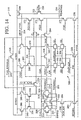
- Fig. 3 is a block diagram of circuitry to be formed in a single integrated circuit chip.
- the chip is an analog signal processing chip designed to acquire and process two-dimensional images, providing cross-correlation information to an external controller, not shown.
- the controller uses the image cross-correlation values to derive X-Y position information.
- the X-Y position information is then used to accurately reconstruct a linear image from the image data acquired using imaging sensor 22 in Fig. 2.
- the navigation sensor 24 is an array having thirty-two rows and sixty-eight columns of photoelements.
- An array of sixty-eight column transfer amplifiers 17 transfers signals in a row-to-row fashion from the navigation sensor 24 to an array of sixty-four DC removal circuits 19.
- it is difficult to illuminate a target area with perfectly consistent light intensity across the entire area to be imaged.
- the ability to provide uniform illumination is often proportional to the cost of the optics and the light source.
- some variations in sensitivity will occur as a result of limitations of integrated circuit processing technology.
- a computational array 21 receives data from the DC removal circuits 19 and performs local difference computations on the data before transferring a cross-correlation output 23 to the off-chip controller. Also shown in Fig. 3 is a source 25 of control logic for the various components of the chip.
- Fig. 4 is a schematic diagram of a photoelement circuit.
- Fig. 5 is a more detailed circuit diagram of a photoelement pair.
- Incoming light is converted into a current that is integrated during a sample period. The stored value is periodically read out, so that it is available for a next step in a processing sequence.
- a reset switch 28 in Fig. 4 is turned “on” momentarily to reset an integration capacitor 30 to 3.25 volts.
- the reset switch 28 is a p-channel transistor that is turned “on” by applying a logic low to the gate of the transistor via a first reset line 32.
- Photocurrent that is generated by means of a photodiode 34 is amplified by a PNP transistor 36.
- the amplified photocurrent charges the integration capacitor 30 downwardly toward a level of 1.75 volts via a transistor 52.
- a read switch 42 is turned “on” to output the stored value along a read line 44 to a transfer amplifier 46.
- the read switch is an n-channel transistor that is controlled by a read control line 48.
- the photodiode 34 of the photoelement 40 generates a current in response to reception of light photons.
- the photodiode is connected to the base of the PNP transistor 36.
- the photodiode may be the base/collector portion of the transistor, so that the transistor is a phototransistor.
- the reverse bias diode capacitance 38 is a parasitic capacitance that may be 0.16 pF.
- the optical power on the photodiode was determined to be 1.1 nW. This causes a current of 0.6 nA in the diode current source. Because of the low current level, amplification is needed to ensure that the optical variation signal, which is only approximately six percent of the base photocurrent for applications in which surface texture is the image of interest, will create sufficient voltage differences to be distinguished from noise.
- the PNP transistor 36 of the photoelement 40 amplifies the photocurrent.
- the amplification provided by the transistor allows use of an integration capacitor 30 that facilitates reproducibility from photoelement to photoelement.
- the low current from the photodiode 34 would require a very small capacitor, e.g., 10 fF, as an integrator in order to get a 2 volt swing. Because of the parasitics, this would be difficult to reproduce on an element-to-element basis.
- Changing the photoelement layout from a diode to a substrate PNP device is a convenient way of providing current amplification.
- a beta value of 18 increases the output emitter current to 11.4 nA.
- an integration capacitor of 0.20 pF can be used. This facilitates reproducibility, but is not so large as to require excessive area.
- a concern with the circuit of Fig. 4 is that a direct beta dependency is introduced into the output current determination and, therefore, the integration capacitor voltage.
- testing has shown that matching of the devices from unit to unit is good, so that the effects of the beta dependency should be minor.
- a servo circuit is formed by three MOS transistors 50, 52 and 54.
- the three MOS transistors form an amplifier with a common gate stage 52 for the output of the phototransistor 36.
- the photodiode reverse voltage i.e., the transistor base voltage
- the photocurrent would be at least partially consumed in charging and discharging the diode capacitance 38 or the transistor basecollector capacitance, rather than providing current to be amplified by the substrate PNP transistor 36.
- the transistor base voltage at the node 56 is kept at a substantially fixed level by the three MOS transistors 50, 52 and 54. While not critical to achieving the desired operation, in the embodiment of Figs. 4 and 5 the substantially fixed voltage level is approximately equal to the NMOS threshold level above AVSS at the collector node 58.
- the three MOS transistors operate as a negative feedback loop by means of transistor 52 operating as a source follower to the emitter node 62 of the PNP transistor.
- the base voltage is controlled by the emitter voltage of the transistor. This is possible because the base voltage, i.e. the photodiode output at capacitor 30, has a very high impedance level.
- Transistor 52 acts as a common gate stage that has an added advantage of providing additional isolation of the emitter node 62 and the base node 56 of the transistor from the voltage swing of a PHTO1 node 64.
- the output voltage at the PHTO1 node 64 is held at 3.25 volts, i.e. VBB1, by the reset switching transistor 28. With the switching transistor electrically "on,” the CGN1 node 66 is held at approximately 2.6 volts and the emitter node 62 is held at approximately 1.4 volts. The base voltage at node 56 is near 1.0 volts.
- a photocurrent of approximately 0.6 nA flows from the base of the transistor 36 to the collector node 58, which is connected to AVSS.
- the reset signal at the first reset line 32 i.e. RST1B
- the output at the PHTO1 node 64 ramps downwardly in a linear manner as the current of the phototransistor 36 emitter is pulled from a capacitive structure formed by the gate-to-channel capacitance of a first n-channel transistor 68 in parallel with a second n-channel transistor 70.
- the transistors 68 and 70 of Fig. 5 are represented by the integration capacitor 30 in Fig. 4.
- the range of voltage of interest is from 3.25 volts to 1.75 volts. Consequently, the gates of the first and second n-channel transistors 68 and 70 are kept sufficiently high that the gate-to-channel capacitance of the devices is above the threshold level of the devices.
- the voltages at the emitter node 62 and the base node 56 remain stabilized by the negative feedback loop described above.
- the voltage at the base node stays within a range of approximately 2 mV.
- read switch 42 is turned “on” with a positive going gate pulse to transistor 42 by means of the read control line 48.
- the positive gate pulse lasts for approximately 200 ns.
- the operation of the transfer amplifier 46 pulls the PHTO1 node 64 down to 1.75 volts. This accomplishes the transfer of the signal from the integration capacitor 30 of Fig. 4 to the capacitor 72 in the transfer amplifier.
- the read control line 48 is caused to return to a logic low and the first reset line 32 is also caused to go low. This turns the reset switch 28 "on,” pulling the PHTO1 node 64 back up to 3.25 volts.
- a particular column transfer amplifier 46 will be described with reference to Fig. 4.
- the read line 44 is shunted to the second input 74 of the amplifier. That is, the two inputs are held at 1.75 volts.
- the output line 108 is connected to a second source of a fixed voltage. While not critical, the voltage at the output line 108 may be 3.25 volts.
- the integration capacitor 30 is also connected to 3.25 volts by means of the reset switch 28.
- the charge across the integration capacitor 30 will vary depending upon the photocurrent generated at the photoelement 40.
- the first input line 76 and the output line 108 of the transfer amplifier are disconnected from the fixed voltage sources of 1.75 volts and 3.25 volts, respectively.
- a positive perturbation is received at the first input line of the transfer amplifier.
- the output of the amplifier will go negative, pulling charge through the transfer capacitor 72 from the read line 44, bringing the voltage value back to 1.75 volts. This is caused by the gain of the amplifier.
- the operation of the computational array 21 of Fig. 3 is a correlation operation. If the initial part of the correlation operation is considered, the difference between signals of two nearest-neighbor photoelements is subtracted. Accurate interpretation of the data requires that the input signals to the computational array are strongly dependent upon the differences in optical illumination received at the various photoelements of the photoreceiver array 24. Consequently, the mismatch of devices resulting from manufacturing differences of devices will cause inaccuracies. Moreover, the integration time for the photoelements is 40 ⁇ s, providing a cycle time for reading out the entire array in the order of 50 ⁇ s. Since CMOS circuitry is preferred in order to achieve low power operation with high circuit density, 1/f noise is also a concern.
- the column transfer amplifier 46 is shown as having the first and second inputs 74 and 76 selectively shunted together by four transistor devices 78, 80, 82 and 84. Two of the transistors operate as switches, while the other two provide a degree of charge injection compensation. The switching of the transistor devices is controlled by a signal at a TRNRST line 86. When the signal on line 86 is high, inputs 74 and 76 are both connected to a source of a fixed voltage via the VBB3 line 88. In the example above, the VBB3 voltage is 1.75 volts. Inverters 110 and 112 provide the proper signal levels to the transistor devices 78-84.
- the signal on line 86 places the transfer amplifier in a reset mode.
- the transfer reset signal connects the inputs 74 and 76 together and simultaneously connects the output line 108 to a source of VBB2, via line 114.
- a second bank of four transistor devices 116 is controlled by the transfer reset signal on TRNRST line 86 in order to connect or disconnect the output line 108 to the source of VBB2.
- the VBB2 voltage is 3.25 volts. The selection of the input and output voltages ensures that the output voltage is centered approximately in the mid range of the operating voltage supply for subsequent stages.
- two of the devices are provided in order to achieve charge injection compensation.
- a third bank 118 of four transistor devices is included in order to selectively connect the output line 108 of the transfer amplifier 46 to a read feedback line 120.
- the third bank 118 and the read feedback line 120 form a portion of an offset adjustment loop. Again, two of the transistors in the bank are present solely for the purpose of charge injection compensation.
- a number of gates 122, 124, 126 and 128 and a clock device 130 are connected to provide proper operation of the second and third banks 116 and 118.
- Each of these devices operates in a conventional manner and may be readily replaced by other conventional circuitry, as will be understood by persons skilled in the art.
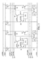
- Fig. 8 shows an offset adjustment amplifier 136 having a first node 138 connected to the VBB2 line 114 and having a second node 140 connected to the read feedback line 120.
- the offset adjustment amplifier 136 is common to all of the column transfer amplifiers 17 of the photoreceiver array 24 of Fig. 3. However, the second node 140 in Fig. 8 is connected to only one transfer amplifier at any given time. In fact, when the sixty-eight column transfer amplifiers are simultaneously in a readout mode, the second node 140 will be electrically isolated from receiving any signals from the transfer amplifiers.
- the voltage state at the read feedback line 120 is compared to the fixed voltage at the VBB2 line 114.
- the voltage states at nodes 138 and 140 will be identical, so that the voltage at output node 142 and at OFA line 144 will be at the nominal output bias level.
- variations in device fabrication and other performance mechanisms will generate offsets.
- the voltage states at nodes 138 and 140 will be different, producing an offset signal that is conducted to the circuitry block 132 via OFA line 144.
- line 144 is connected to the column transfer amplifier 46 to provide offset compensation of the transfer amplifier.
- the OFA line 144 is connected to the transfer amplifier 46 at an offset correction port 146, as shown in Fig. 7.
- Fig. 9 the internal circuitry of the transfer amplifier 46 is shown. Part of the circuitry of Fig. 9 is conventional and is readily understood by persons skilled in the art. Such conventional circuitry will not be explained herein. However, added to the conventional circuitry is an offset sample-and-hold circuit 148 that is accessed by the offset correction port 146 of the transfer amplifier. At the end of a reset operation in which the particular transfer amplifier is connected to the offset adjustment amplifier 136 of Fig. 8, the sample-and-hold circuit is refreshed.
- a signal received at a refresh port 150 of the transfer amplifier properly biases a fourth bank of transistor devices 152 for connecting the offset correction port 146 to OFAM line 154.
- the OFAM line 154 leads to a pair of transistors that combine to operate as a storage capacitor for the offset adjustment signal.
- a third transistor 160 is biased by the offset correction signal to provide offset compensation to the conventional circuitry of the transfer amplifier.
- the offset correction is achieved by forming a loop that originates at the output line 108 of the transfer amplifier 46 and continues to the offset correction port 146 of the transfer amplifier.
- VBB3 e.g. 1.75 volts
- VBB2 e.g. 3.25 volts
- the offset control operation is initiated by connecting the output line 108 to the read feedback line 120 by means of the third bank 118 of transistor devices.
- the voltage state at the read feedback line 120 will be equal to VBB2.
- the offset adjustment amplifier 136 compares the voltage at the read feedback line 120 to the anticipated voltage state, i.e. the VBB2 voltage.
- the amplifier 136 is a differential cell having an output node 142 connected to the offset adjustment line 144.
- This offset adjustment line completes the loop by connecting to the offset correction port 146 of the transfer amplifier 46, as shown in Figs. 8 and 9.
- the fourth bank 152 of transistor devices allows the signal at the offset correction port 146 to be stored by means of transistors 156 and 158. The stored charge provides offset correction to the transfer amplifier circuitry until the next refresh interval.
- each column transfer amplifier 46 is sequentially connected to the photoelements in a particular row of photoelements. In one embodiment, there are sixty-eight columns and thirty-two rows of photoelements.
- Fig. 10 illustrates five of the columns 162, 164, 166, 168 and 170, with each column being selectively connected to a different transfer amplifier 46, 172, 174, 176 and 178.
- the photoelement 40 of Fig. 4 is shown as being paired with a second photoelement 102 from the same column. Consequently, each photoelement is connected to the same read line 44 by means of turning "on" a read switch 42 and 101.
- Read control lines 48 and 90 provide individual control of the read switches, so that no two photoelements will be connected to the transfer amplifier simultaneously.
- reset devices 28 and 92 that are connected to separate reset lines 32 and 94 and to the separate PHTO nodes 64 and 96.
- the second photoelement includes its own common gate arrangement provided by MOS transistors 98, 99 and 100 that operate in the same manner as the MOS transistors 50, 52 and 54 of the first photoelement 40.
- the second photoelement includes storage-capacitive transistors 104 and 106 that operate as the integration capacitor for the second photoelement.
- the integration time for the photoelements 40 and 102 in each column 162-170 is approximately 40 ⁇ s.
- the read switch 42 of the first row of photoelements 40 is closed, so that each transfer capacitor 72 of the various transfer amplifiers 46, 172, 174, 176 and 178 receives a charge corresponding to the light energy that strikes the photoelement 40 in the first row.
- the received charge is transferred to subsequent processing circuitry via output lines 108, 180, 182, 184 and 186.
- the readout time of a single row is estimated to be between 200 ns and 300 ns.
- the read switches 42 are opened and the read switches 101 of the second row of photoelements 102 are closed. The process is repeated until each row of photoelements is read.
- the offset adjustment operation described above requires no more than 4 ⁇ s. Therefore, at least eight transfer amplifiers 46 and 172-178 can be connected to the offset adjustment amplifier 136 of Fig. 8 in a sequential manner during each 40 ⁇ s integration interval in which the transfer amplifiers are idle between transfer operations.
- the sample-and-hold circuit 148 of each transfer amplifier is designed to ensure that there is no significant voltage droop at the storage capacitance provided by transistors 156 and 158. Thus, reset can occur without a time sacrifice with respect to transferring photoelement signals.
- a concern in the processing of signals from the navigation array 24 of photoelements through the computational array 21 of Fig. 3 involves potential corruption of the processing as a result of a characteristic that is common within a neighborhood of photoelements.
- a scanner may have a source for illuminating the substrate as the scanner is moved relative to an original. It is difficult to illuminate an entire viewing region without variations in illumination. Signal processing may be adversely affected by such variations.
- the DC removal circuits 19 of Fig. 3 have the basic function of removing low spatial frequency variations within the neighborhood of photoelements. As noted above, the DC removal circuits may also have a low-pass characteristic that may be set to remove spatial frequency components at high frequencies. Thus, the DC removal circuits can have a band pass characteristic.
- the DC removal circuits transform the original image into an image of local differences. The local differences approach results in the original image being destroyed, but for applications such as the determination of scanner movement relative to an original, this is not a concern. The removal of low spatial frequencies maintains the integrity of correlation signals. Moreover, the local differences approach has the additional advantage of reducing the dynamic range requirements of the computation array 21, which actually calculates the image cross-correlations.
- the removal of low spatial frequencies renders the navigation operation less susceptible to such things as the navigation sensor being positioned so that one major region of the array views paper fibers of a shaded region of a scanned original, while the paper fibers viewed by a second portion of the array are outside of the shaded region.
- each switching network gates its inputs through a series of switches controlled by digital control inputs from the control logic 25 of Fig. 3.
- the outputs of each switching network 198-206 are connected to an associated DC removal amplifier 208, 210 and 212.
- the DC removal circuits may be in any one of a number of modes, including a test mode and a DC removal disabled mode.
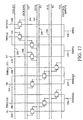
- the DC removal amplifier 210 of Fig. 11 an example of four possible modes of operation of the DC removal amplifier 210 of Fig. 11 are characterized.
- NODCR no DC removal
- the output 236 of the amplifier 210 is the same as the input INP, which is connected directly to the photoreceiver output line 192 by the switching network 202.
- TST test
- the output signal of the DC removal amplifier is dependent upon three known test outputs: TC, TL and TR.
- the switching network 202 is not connected to the nearest neighbor photoreceivers, a wider sampling for removing low frequency information is acquired.
- the "primary input" in the F1 and F2 modes is the PHR(i) output, and local differencing is achieved by the subtraction of secondary inputs from PHR(i+2) and PHR(i-2).
- the switching network 202 receives inputs from photoreceiver outputs 188 and 196, which are the photoreceivers removed by two from the photoreceiver of interest.
- the photoreceiver outputs are received via the transfer amplifiers described previously.
- DCRCM DC removal common mode
- the switching network is configured by setting a binary input pair CFIG1 222 and CFIGO 224 to one of four possible combinations.
- a calibration signal may be received at CAL line 226.
- the CAL signal is used to provide a condition in which only the INP(i) line 228 conducts a signal from the switching network 202 to the DC removal amplifier 210.
- the CAL signal disconnects the DIN outputs 230, 232 and 234 during an offset correction operation that is separate from the offset control operation of the transfer amplifiers.
- the circuitry of Figs. 11-13 can be configured on one of four ways by controlling the configuration signals at lines 222 and 224.
- a first mode DC removal is disabled.
- the DIN signals along outputs 230, 232 and 234 are not utilized in this mode, since gates 242 and 252 in Fig. 13 do not provide the required DC removal enable signals at lines 244-250, 256 and 258.
- the configuration signals at lines 222 and 224 define a test mode in which gate 242 provides enabling signals at lines 244 and 246.
- the DCRCM common mode input 220 is passed through the switching network 202 to INP(i) line 228.
- Test inputs TL 214, TR 216 and TC 218 are passed through to outputs 234, 232 and 230, respectively.
- the test inputs are known signals, allowing complete characterization of the DC removal amplifier 210.
- a third configuration of the switching network 202 is referred to as the DC removal function 1 mode.
- This third mode is enabled by providing a logic high at line 250 and a logic low at line 248 by means of gate 252.
- the fourth configuration is referred to as a DC removal function 2 mode.
- the F2 mode connects the DINM1(i) output 232 to the PHR(i+2) line 196.
- Gate 254 triggers the proper signals along lines 256 and 258 for enabling the F2 mode.
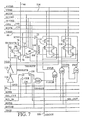
- the DC removal amplifier 210 is shown in Fig. 14.
- the amplifier includes a first differential cell Ay 260 and a second differential cell Ax 262.
- the INP(i) output 228 is received at the second differential cell, while the other three outputs 230, 232 and 234 from Fig. 12 are received at the first differential cell.
- the second differential cell 262 includes a differential pair of transistors 264 and 266.
- Transistors 268 and 270 provide a current mirror load for transistors 264 and 266.
- a folded cascode output stage is formed by four serially connected transistors 272, 274, 276 and 278.
- transistors 280 and 282 are biased by voltages NCON4 and PCON4 to act as constant current sources. These two voltages, as well as bias voltages VBP and VBN, are generated and provided by constant voltage sources.
- the DC removal amplifier 210 includes offset correction circuitry.
- Transistors 284 acts as a switch to achieve unity gain feedback.
- Offset correction transistors 286, 288, 290 and 292 are biased in the triode region to introduce offset correction into the amplifier.
- the other four transistors in the bank 300 are used as switches to selectively shunt the gain degeneration resistive transistors and are under the control of the G1 and G2 digital gain control inputs.
- the G1 and G2 voltages are set by the control logic 25 shown in Fig. 3.
- the four resistive transistors 302, 304, 306 and 308 may be referred to as r 302 , r 304 , r 306 and r 308 , respectively.
- the values G1 and G2 are the boolean complements of the digital control inputs G1 and G2 and have values of 0 or 1.
- the values of the degeneration resistors r 302 -r 308 are modulated by varying the control voltage input GAINADJ signal at line 310.
- switching network 202 of Figs. 12 and 13 may be used to set the DC removal amplifier 210 in any one of four modes.
- Fig. 15 is the table which summarizes the transfer characteristics of the circuitry in each of the four modes.
- the DC removal modes of F1 and F2 low spatial frequency components of the photoreceiver output 192 of Fig. 11 are removed in effect by subtracting from a signal of interest the average of the signals received by a DC removal amplifier 210 from two or more photoreceivers.
- the signal of interest is the PHR(i) signal from line 192. This signal is received at the DINP(i) line 230 in Fig. 14.
- PHR(i) is shown as being multiplied by two in the equation of the F1 mode.
- the signal from PHR(i-2) is switched to both the DINM1(i) line 232 and the DINM0(i) line 234, so that PHR(i-2) is also multiplied by two.
- the difference value is multiplied by gm y /gm x , which is subtracted from the DCRCM value.
- the DCRCM value is selected to establish a positive mid range voltage value for subsequent processing of the analog signal at WDATA(i) line 236.
- the signals at the INP(i) line 228, the DINP(i) line 230 and DINM0(i) line 234 remain the same, but the DINM1(i) line 232 is switched from connection with the PHR(i-2) output line 188 to the PHR(i+2) line 196.
- the filtering of common components occurs, but the commonality is with reference to three photoreceivers, rather than two.
- Photoreceiver PHR(i) controls transistors 314 and 316.
- Photoreceiver PHR(i-2) controls transistor 318, while photoreceiver PHR(i+2) controls transistor 320.
- the number of transistors controlled by each photoreceiver, or the areas of such transistors, can be varied to vary the weighting of the different photoreceivers.
- Figs. 16 and 17 provide a modification of the F2 mode.
- the signal from a photoreceiver is conducted without delay to the line 192.
- the signal along 192 is in real time (t).
- a pair of delay circuits 290 and 292 is connected in series along a second line 294.
- the signal at the line 294 is the photoreceiver output with a delay of 2 ⁇ .
- the delay circuits 290 and 292 along the second line 294 allow two-dimensional DC removal. That is, a secondary input for DC removal may be from a different row within the same column as the source of the primary input.
- the circuit of Fig. 17 is used to implement the F2 mode of operation. Common lines in Figs. 12 and 17 are identified by identical reference numerals.
- the circuit of Fig. 17 remains the same with respect to the primary input at line 192 and one of the secondary inputs at line 188.
- the secondary input at line 294 is from the same transfer amplifier as the primary input at line 192.
- the input is from the same column, but the delay of 2 ⁇ results in the secondary input being from a different row.
- the delay ⁇ is equal to the sampling time of the transfer amplifiers.
- delay circuits 290 and 292 in Fig. 16 are not critical to the operation of the two-dimensional DC removal function.
- the appropriate secondary inputs may be provided by sample-and-hold circuits that operate in a round robin fashion.
- Figs. 12-14 and Figs. 16 and 17 efficiently overcome the adverse effects of variations in illumination of a substrate that is viewed by a photoreceiver array. Moreover, in the use of the invention in providing navigation information, as set forth above, the navigation operation is less affected by such things as one portion of a navigation array viewing paper fibers of a shaded region of a scanned original, while the paper fibers viewed by a second portion of the array are outside of the shaded region of the original.
- the DC removal amplifier 210 of Fig. 14 includes offset correction to reduce voltage offsets, such as those generated by manufacturing-induced variations in device parameters.
- Transistors 322, 324, 326, 328, 330 and 332 are employed to implement offset correction.
- transistor 322 is switched “on” with the CAL input signal at line 226, thereby connecting the DC removal amplifier output WDATA(i) to an OFST_CTRL node 334.
- the negative feedback as shown by line 298 in Fig. 11 at the second differential cell 262 is disconnected by turning "off” transistor 284.
- the differential inputs to the cells 260 and 262 are shorted out by the shunt switch transistors 328, 330 and 332.
- the DC removal amplifier 210 amplifies the input offset. Offset correction transistors 286, 288, 290 and 292 are biased in the triode region. If the voltage at OFST_CTRL node 334 is not equal to bias voltage VBP, current mirrors provided by transistors 268 and 270 and transistors 336 and 338 will be unbalanced and will create an additional voltage at the WDATA(i) output 236.
- a o1 being the open loop gain of the amplifier 210 from the conventional inputs
- the amplifier is designated to have the following relationship between the OFST_CTRL node and the output 236:
- WDATA i A 01 100 ⁇ vbs - OFST_CTRL
- the temporary negative feedback path created by means of transistor 322 causes a signal equal to 100 times the input offset to be developed between OFST_CTRL and the bias voltage VBP.
- the CAL input is brought to logic low, so that the OFST_CTRL node 334 is disconnected from the WDATA(i) output 236.
- Transistor 324 is used as a capacitor approximately equal to 300 fF.
- the offset correction signal generated during the correction cycle is stored as charge at the gate of the transistor 324. If desired, offset correction may be disabled by driving the gate of transistor 326 low via line 340, thereby shunting the OFST_CTRL node 334 to the bias input VBP.
Landscapes
- Engineering & Computer Science (AREA)
- Multimedia (AREA)
- Signal Processing (AREA)
- Power Engineering (AREA)
- Transforming Light Signals Into Electric Signals (AREA)
- Facsimile Scanning Arrangements (AREA)
- Facsimile Heads (AREA)
- Light Receiving Elements (AREA)
- Amplifiers (AREA)
Applications Claiming Priority (3)
| Application Number | Priority Date | Filing Date | Title |
|---|---|---|---|
| US08/591,076 US5703353A (en) | 1996-01-25 | 1996-01-25 | Offset removal and spatial frequency band filtering circuitry for photoreceiver signals |
| US591076 | 1996-01-25 | ||
| EP97300163A EP0786899B1 (en) | 1996-01-25 | 1997-01-13 | Image signal read-out circuitry with offset correction |
Related Parent Applications (1)
| Application Number | Title | Priority Date | Filing Date |
|---|---|---|---|
| EP97300163A Division EP0786899B1 (en) | 1996-01-25 | 1997-01-13 | Image signal read-out circuitry with offset correction |
Publications (2)
| Publication Number | Publication Date |
|---|---|
| EP1175090A1 EP1175090A1 (en) | 2002-01-23 |
| EP1175090B1 true EP1175090B1 (en) | 2007-04-25 |
Family
ID=24364959
Family Applications (2)
| Application Number | Title | Priority Date | Filing Date |
|---|---|---|---|
| EP01117841A Expired - Lifetime EP1175090B1 (en) | 1996-01-25 | 1997-01-13 | Signal transfer circuitry with offset correction |
| EP97300163A Expired - Lifetime EP0786899B1 (en) | 1996-01-25 | 1997-01-13 | Image signal read-out circuitry with offset correction |
Family Applications After (1)
| Application Number | Title | Priority Date | Filing Date |
|---|---|---|---|
| EP97300163A Expired - Lifetime EP0786899B1 (en) | 1996-01-25 | 1997-01-13 | Image signal read-out circuitry with offset correction |
Country Status (4)
| Country | Link |
|---|---|
| US (2) | US5703353A (enExample) |
| EP (2) | EP1175090B1 (enExample) |
| JP (2) | JP3956242B2 (enExample) |
| DE (2) | DE69737665T2 (enExample) |
Families Citing this family (27)
| Publication number | Priority date | Publication date | Assignee | Title |
|---|---|---|---|---|
| US6256016B1 (en) | 1997-06-05 | 2001-07-03 | Logitech, Inc. | Optical detection system, device, and method utilizing optical matching |
| US6025935A (en) * | 1997-12-31 | 2000-02-15 | Peripheral Imaging Corporation | Charge storage image scanner having equalizing pre-charge and reset improvements |
| US6233368B1 (en) * | 1998-03-18 | 2001-05-15 | Agilent Technologies, Inc. | CMOS digital optical navigation chip |
| US6002124A (en) * | 1998-03-20 | 1999-12-14 | Hewlett-Packard Company | Portable image scanner with optical position sensors |
| US6118132A (en) * | 1998-09-17 | 2000-09-12 | Agilent Technologies | System for measuring the velocity, displacement and strain on a moving surface or web of material |
| US6188058B1 (en) | 1998-09-17 | 2001-02-13 | Agilent Technologies Inc. | System for taking displacement measurements having photosensors with imaged pattern arrangement |
| US6304826B1 (en) * | 1999-02-05 | 2001-10-16 | Syscan, Inc. | Self-calibration method and circuit architecture of image sensor |
| US6246050B1 (en) | 1999-03-08 | 2001-06-12 | Hewlett-Packard Company | Optical encoders using non-patterned targets |
| US6633332B1 (en) | 1999-05-13 | 2003-10-14 | Hewlett-Packard Development Company, L.P. | Digital camera system and method capable of performing document scans |
| US6362465B1 (en) | 1999-06-14 | 2002-03-26 | Hewlett-Packard Company | Optical scanning system and method capable of receiving inputs from a user |
| US6975355B1 (en) | 2000-02-22 | 2005-12-13 | Pixim, Inc. | Multiple sampling via a time-indexed method to achieve wide dynamic ranges |
| US6312124B1 (en) | 1999-10-27 | 2001-11-06 | Hewlett-Packard Company | Solid and semi-flexible body inkjet printing system |
| US6297984B1 (en) * | 1999-12-29 | 2001-10-02 | Tower Semiconductor Ltd. | Structure and method for protecting integrated circuits during plasma processing |
| US7161578B1 (en) | 2000-08-02 | 2007-01-09 | Logitech Europe S.A. | Universal presentation device |
| US7035932B1 (en) * | 2000-10-27 | 2006-04-25 | Eric Morgan Dowling | Federated multiprotocol communication |
| US6781570B1 (en) | 2000-11-09 | 2004-08-24 | Logitech Europe S.A. | Wireless optical input device |
| US6657487B2 (en) | 2001-02-05 | 2003-12-02 | Em(Us) Design, Inc | Photodetector preamplifier circuit having a rotating input stage |
| US7333083B1 (en) | 2001-05-10 | 2008-02-19 | Logitech Europe S.A. | Optical based performance improvement for an optical illumination configuration |
| US6617565B2 (en) * | 2001-11-06 | 2003-09-09 | Omnivision Technologies, Inc. | CMOS image sensor with on-chip pattern recognition |
| US6788875B1 (en) | 2002-04-08 | 2004-09-07 | Logitech Europe S.A. | Suspension system for use in an optical displacement detection system |
| US7131751B1 (en) | 2002-04-12 | 2006-11-07 | Logitech, Inc. | Attachment system for use in an optical illumination system |
| US6876233B1 (en) | 2003-02-15 | 2005-04-05 | Medtronics, Inc. | DC cancellation apparatus and method |
| US7515188B2 (en) * | 2004-07-16 | 2009-04-07 | Micron Technology, Inc. | Method and system for reducing mismatch between reference and intensity paths in analog to digital converters in CMOS active pixel sensors |
| KR100790259B1 (ko) | 2005-12-14 | 2008-01-02 | 매그나칩 반도체 유한회사 | 아날로그 디지털 컨버터, 이를 구비한 시모스 이미지 센서및 아날로그 옵셋 제거방법 |
| JP4978022B2 (ja) * | 2006-02-16 | 2012-07-18 | 富士通セミコンダクター株式会社 | 演算増幅器 |
| JP5495864B2 (ja) * | 2010-03-08 | 2014-05-21 | キヤノン株式会社 | 光電変換装置 |
| JP5360270B2 (ja) * | 2011-12-07 | 2013-12-04 | 凸版印刷株式会社 | 液晶表示装置 |
Family Cites Families (13)
| Publication number | Priority date | Publication date | Assignee | Title |
|---|---|---|---|---|
| US3937874A (en) * | 1975-01-09 | 1976-02-10 | General Electric Company | Offset voltage correction circuit for multiple video channel imager |
| US4409483A (en) * | 1980-10-07 | 1983-10-11 | Westinghouse Electric Corp. | Radiant energy differential sensor system |
| US4400729A (en) * | 1980-12-03 | 1983-08-23 | Jones George R | Pseudo-DC restore application to staring array detectors |
| DE3049043A1 (de) * | 1980-12-24 | 1982-07-15 | Robert Bosch Gmbh, 7000 Stuttgart | Verfahren und anordnung zur unterdrueckung des niederfrequenten rauschens bei ausgangssignalen von halbleiter- sensoren |
| JPS6152012A (ja) * | 1984-08-22 | 1986-03-14 | Hitachi Ltd | 差動増幅回路 |
| US4884039A (en) * | 1988-09-09 | 1989-11-28 | Texas Instruments Incorporated | Differential amplifier with low noise offset compensation |
| US4940981A (en) * | 1989-02-08 | 1990-07-10 | Burr-Brown Corporation | Dual analog-to-digital converter with single successive approximation register |
| JP2931088B2 (ja) * | 1990-11-30 | 1999-08-09 | キヤノン株式会社 | マルチチップ型光電変換装置 |
| US5149980A (en) * | 1991-11-01 | 1992-09-22 | Hewlett-Packard Company | Substrate advance measurement system using cross-correlation of light sensor array signals |
| JPH05219440A (ja) * | 1992-02-07 | 1993-08-27 | Olympus Optical Co Ltd | 画像入力装置 |
| JP2988795B2 (ja) * | 1992-05-29 | 1999-12-13 | シャープ株式会社 | 受光増幅装置 |
| US5352884A (en) * | 1993-04-14 | 1994-10-04 | General Electric Corporation | Method and apparatus for providing offset for light detector |
| FR2728420B1 (fr) * | 1994-12-16 | 1997-01-24 | Thomson Csf | Procede de compensation electronique des non-uniformites dans la detection d'images, en particulier infrarouge, et circuit de correction pour sa mise en oeuvre |
-
1996
- 1996-01-25 US US08/591,076 patent/US5703353A/en not_active Expired - Lifetime
-
1997
- 1997-01-07 JP JP00082897A patent/JP3956242B2/ja not_active Expired - Lifetime
- 1997-01-13 DE DE69737665T patent/DE69737665T2/de not_active Expired - Lifetime
- 1997-01-13 DE DE69730367T patent/DE69730367T2/de not_active Expired - Lifetime
- 1997-01-13 EP EP01117841A patent/EP1175090B1/en not_active Expired - Lifetime
- 1997-01-13 EP EP97300163A patent/EP0786899B1/en not_active Expired - Lifetime
- 1997-09-05 US US08/924,161 patent/US5900625A/en not_active Expired - Lifetime
-
2003
- 2003-12-26 JP JP2003434480A patent/JP4027308B2/ja not_active Expired - Lifetime
Also Published As
| Publication number | Publication date |
|---|---|
| DE69737665T2 (de) | 2007-12-27 |
| US5703353A (en) | 1997-12-30 |
| JP2004120801A (ja) | 2004-04-15 |
| US5900625A (en) | 1999-05-04 |
| DE69730367D1 (de) | 2004-09-30 |
| JPH10136149A (ja) | 1998-05-22 |
| EP1175090A1 (en) | 2002-01-23 |
| EP0786899A3 (en) | 1998-10-14 |
| EP0786899A2 (en) | 1997-07-30 |
| DE69730367T2 (de) | 2005-09-01 |
| DE69737665D1 (de) | 2007-06-06 |
| EP0786899B1 (en) | 2004-08-25 |
| JP3956242B2 (ja) | 2007-08-08 |
| JP4027308B2 (ja) | 2007-12-26 |
Similar Documents
| Publication | Publication Date | Title |
|---|---|---|
| EP1175090B1 (en) | Signal transfer circuitry with offset correction | |
| US5769384A (en) | Low differential light level photoreceptors | |
| US5488415A (en) | Solid-state image pickup device having a photoelectric conversion detection cell with high sensitivity | |
| US7133074B1 (en) | Image sensor circuits including sampling circuits used therein for performing correlated double sampling | |
| EP1178673B1 (en) | Solid state image pickup apparatus | |
| US6130423A (en) | Method and apparatus for a CMOS image sensor with a distributed amplifier | |
| US5729008A (en) | Method and device for tracking relative movement by correlating signals from an array of photoelements | |
| US7924332B2 (en) | Current/voltage mode image sensor with switchless active pixels | |
| EP0164222A1 (en) | Pixel non-uniformity correction system | |
| KR20190022467A (ko) | 샘플-앤드-홀드 기반 시간적 대비 비전 센서 | |
| US20010033337A1 (en) | Image pickup apparatus | |
| US20030164443A1 (en) | Image sensor | |
| JPH09233259A5 (enExample) | ||
| KR20010109157A (ko) | Mos 기반 이미지 센서 및 이를 위한 흑 레벨 신호를형성하는 방법 | |
| US6104020A (en) | Electronic shutter for a low differential light level photo-receiver cell | |
| Wang et al. | CMOS video cameras | |
| US6188057B1 (en) | Method and apparatus for testing photo-receiver arrays and associated read channels | |
| JP3571934B2 (ja) | イメージセンサー | |
| US4454435A (en) | CCD Amplifier using second correlated sampling and negative feedback for noise reduction | |
| US6191412B1 (en) | Gain and error correction circuitry | |
| EP0880851B1 (en) | Apparatus for reading and processing image information | |
| US20030094565A1 (en) | Systems and methods of sampling a photodetector and photocell circuits incorporating the same | |
| US6552324B1 (en) | Selectable pixel amplifier for use in a photosensor array | |
| US6952226B2 (en) | Stray-insensitive, leakage-independent image sensing with reduced sensitivity to device mismatch and parasitic routing capacitance | |
| JPH08116491A (ja) | 光電変換装置 |
Legal Events
| Date | Code | Title | Description |
|---|---|---|---|
| PUAI | Public reference made under article 153(3) epc to a published international application that has entered the european phase |
Free format text: ORIGINAL CODE: 0009012 |
|
| 17P | Request for examination filed |
Effective date: 20010802 |
|
| AC | Divisional application: reference to earlier application |
Ref document number: 786899 Country of ref document: EP |
|
| AK | Designated contracting states |
Kind code of ref document: A1 Designated state(s): DE FR GB |
|
| RIN1 | Information on inventor provided before grant (corrected) |
Inventor name: HORNAK, THOMAS Inventor name: BLALOCK, TRAVIS N. Inventor name: BEARD, DAVID Inventor name: BAUMGARTNER, RICHARD A. |
|
| AKX | Designation fees paid |
Free format text: DE FR GB |
|
| 17Q | First examination report despatched |
Effective date: 20020906 |
|
| RAP1 | Party data changed (applicant data changed or rights of an application transferred) |
Owner name: AGILENT TECHNOLOGIES, INC. (A DELAWARE CORPORATION |
|
| GRAP | Despatch of communication of intention to grant a patent |
Free format text: ORIGINAL CODE: EPIDOSNIGR1 |
|
| RAP1 | Party data changed (applicant data changed or rights of an application transferred) |
Owner name: AGILENT TECHNOLOGIES, INC. |
|
| GRAS | Grant fee paid |
Free format text: ORIGINAL CODE: EPIDOSNIGR3 |
|
| GRAA | (expected) grant |
Free format text: ORIGINAL CODE: 0009210 |
|
| AC | Divisional application: reference to earlier application |
Ref document number: 0786899 Country of ref document: EP Kind code of ref document: P |
|
| AK | Designated contracting states |
Kind code of ref document: B1 Designated state(s): DE FR GB |
|
| REG | Reference to a national code |
Ref country code: GB Ref legal event code: FG4D |
|
| REF | Corresponds to: |
Ref document number: 69737665 Country of ref document: DE Date of ref document: 20070606 Kind code of ref document: P |
|
| ET | Fr: translation filed | ||
| PLBE | No opposition filed within time limit |
Free format text: ORIGINAL CODE: 0009261 |
|
| STAA | Information on the status of an ep patent application or granted ep patent |
Free format text: STATUS: NO OPPOSITION FILED WITHIN TIME LIMIT |
|
| 26N | No opposition filed |
Effective date: 20080128 |
|
| REG | Reference to a national code |
Ref country code: GB Ref legal event code: 732E |
|
| REG | Reference to a national code |
Ref country code: FR Ref legal event code: TP |
|
| REG | Reference to a national code |
Ref country code: FR Ref legal event code: RM |
|
| REG | Reference to a national code |
Ref country code: GB Ref legal event code: 732E Free format text: REGISTERED BETWEEN 20101007 AND 20101013 |
|
| PGFP | Annual fee paid to national office [announced via postgrant information from national office to epo] |
Ref country code: GB Payment date: 20141230 Year of fee payment: 19 |
|
| PGFP | Annual fee paid to national office [announced via postgrant information from national office to epo] |
Ref country code: FR Payment date: 20141226 Year of fee payment: 19 |
|
| PGFP | Annual fee paid to national office [announced via postgrant information from national office to epo] |
Ref country code: DE Payment date: 20150126 Year of fee payment: 19 |
|
| REG | Reference to a national code |
Ref country code: DE Ref legal event code: R119 Ref document number: 69737665 Country of ref document: DE |
|
| GBPC | Gb: european patent ceased through non-payment of renewal fee |
Effective date: 20160113 |
|
| REG | Reference to a national code |
Ref country code: FR Ref legal event code: ST Effective date: 20160930 |
|
| PG25 | Lapsed in a contracting state [announced via postgrant information from national office to epo] |
Ref country code: DE Free format text: LAPSE BECAUSE OF NON-PAYMENT OF DUE FEES Effective date: 20160802 Ref country code: GB Free format text: LAPSE BECAUSE OF NON-PAYMENT OF DUE FEES Effective date: 20160113 |
|
| PG25 | Lapsed in a contracting state [announced via postgrant information from national office to epo] |
Ref country code: FR Free format text: LAPSE BECAUSE OF NON-PAYMENT OF DUE FEES Effective date: 20160201 |