EP1174711A2 - Ionenselektive Elektrode - Google Patents
Ionenselektive Elektrode Download PDFInfo
- Publication number
- EP1174711A2 EP1174711A2 EP01116797A EP01116797A EP1174711A2 EP 1174711 A2 EP1174711 A2 EP 1174711A2 EP 01116797 A EP01116797 A EP 01116797A EP 01116797 A EP01116797 A EP 01116797A EP 1174711 A2 EP1174711 A2 EP 1174711A2
- Authority
- EP
- European Patent Office
- Prior art keywords
- ion selective
- electrode
- selective membrane
- layer
- material layer
- Prior art date
- Legal status (The legal status is an assumption and is not a legal conclusion. Google has not performed a legal analysis and makes no representation as to the accuracy of the status listed.)
- Withdrawn
Links
Images
Classifications
-
- G—PHYSICS
- G01—MEASURING; TESTING
- G01N—INVESTIGATING OR ANALYSING MATERIALS BY DETERMINING THEIR CHEMICAL OR PHYSICAL PROPERTIES
- G01N27/00—Investigating or analysing materials by the use of electric, electrochemical, or magnetic means
- G01N27/26—Investigating or analysing materials by the use of electric, electrochemical, or magnetic means by investigating electrochemical variables; by using electrolysis or electrophoresis
- G01N27/28—Electrolytic cell components
- G01N27/30—Electrodes, e.g. test electrodes; Half-cells
- G01N27/333—Ion-selective electrodes or membranes
-
- G—PHYSICS
- G01—MEASURING; TESTING
- G01N—INVESTIGATING OR ANALYSING MATERIALS BY DETERMINING THEIR CHEMICAL OR PHYSICAL PROPERTIES
- G01N27/00—Investigating or analysing materials by the use of electric, electrochemical, or magnetic means
- G01N27/26—Investigating or analysing materials by the use of electric, electrochemical, or magnetic means by investigating electrochemical variables; by using electrolysis or electrophoresis
- G01N27/28—Electrolytic cell components
- G01N27/30—Electrodes, e.g. test electrodes; Half-cells
- G01N27/307—Disposable laminated or multilayered electrodes
Definitions
- This invention relates to an ion selective electrode favorably employable for analysis of ionic components in a whole blood sample or a serum sample.
- An ion selective electrode is widely employed for analyzing ionic components in a liquid sample such as a whole blood sample or a serum sample.
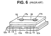
- the ion selective electrode comprises a non-electroconductive support 11, a pair of electrodes each of which comprises a silver metal layer 12a, 12b and a silver halide layer 13a, 13b, an electrolytic material layer 14, an ion selective membrane 15, and a non-electroconductive cover sheet 16 having a pair of openings 17a, 17b for receiving a sample solution and a reference solution, respectively, each opening being placed above each electrode unit, and having thereon an a bridge member 17 for electrically connecting the sample solution received in one opening and the reference solution received in another opening.
- the ion selective electrode such as that illustrated in Fig. 6 is generally manufactured in a mass scale, by the steps of:
- the above-described industrial method is advantageous for manufacturing a great number of ion selective electrodes in a mass scale.
- United States Patent No. 4,789,435 describes an ion selective electrode assembly comprising plural ion selective electrodes for analyzing plural ionic components such as Na + , K + , and Cl - , simultaneously.
- one of plural ion selective electrodes has an ion selective membrane differing from that of other ion selective electrode in chemical composition.
- the ion selective membrane comprises a combination of specifically selected materials, and the materials are very expensive.
- the object of the invention also resides in providing a method of manufacturing ion selective electrodes having satisfactory analytical performance in a mass scale at a relatively low production cost.
- the present invention resides in an ion selective electrode comprising, in order, a non-electroconductive support, a pair of electrodes each of which comprises a silver metal layer and a silver halide layer, an electrolytic material layer, an ion selective membrane, and a non-electroconductive sheet having a pair of openings for receiving a sample solution and a reference solution, respectively, each opening being placed above each electrode, and having thereon a bridge member for electrically connecting the sample solution received in one opening and the reference solution received in another opening, which is characterized in that the ion selective membrane is divided into two separate portions, one of which is placed in a position above one electrode and another of which is placed in a position above another electrode.
- the ion selective electrode of the invention is preferably manufactured in a mass scale by the method comprising the steps of:
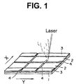
- Fig. 1 illustrates an initial procedure (division of electrode layer into several electrode potions) for manufacturing ion selective electrodes according to the present invention.
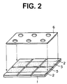
- Fig. 2 illustrates a procedure of placing a mask having openings on an electrolytic material layer coated on the electrode layer divided into plural portions in the procedure of Fig. 1.
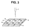
- Fig. 3 illustrates a procedure of placing a solution of ion selective membrane material in openings of the mask placed on the electrolytic material layer in the procedure of Fig. 2.
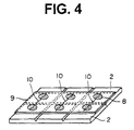
- Fig. 4 illustrates a procedure of placing a non-electroconductive sheet having a pair of openings for receiving a sample solution and a reference solution, respectively, each opening being placed above each electrode.
- the non-electroconductive sheet further has thereon a bridge member for electrically connecting the sample solution received in one opening and the reference solution received in another opening.
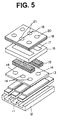
- Fig. 5 schematically illustrates a typical structure of an ion selective electrode assembly of the invention comprising plural ion selective electrodes for analyzing plural ionic components simultaneously.
- Fig. 6 illustrates a representative structure of a conventional ion selective electrode.
- a continuous longitudinal polymer sheet having thereon a silver metal layer For manufacturing the ion selective electrodes in a mass scale, a continuous longitudinal polymer sheet having thereon a silver metal layer.
- the silver metal layer is generally placed on the polymer sheet by a deposition process.
- the polymer sheet generally is a polyethylene terephthalate sheet.
- On both side areas of the silver metal layer are coated with a polymer film for protecting the silver metal layer in the coated area from oxidization in the following chemical processing procedure.
- the polymer film can be produced from a film-forming resist resin solution.
- slits or scratches
- Every slit 4 divides the silver metal layer 2 to portions which are electrically insulated from each other.
- One slit is provided to extend in the longitudinal direction (Y-direction), and other slits are provided to extend in directions (X-directions) traversing the Y-direction.
- the slits in the X-direction are provided to separate ion selective electrode units.
- three ion selective electrode units are produced.
- the slit in the Y-direction is provided to separate the electrode layer in one electrode unit to give two electrode portions, one of which is to potentiometrically detect a target ionic component in a sample solution, while another is to potentiometrically detect the same ionic component in a reference solution.
- the slits can be provided by applying a laser beam onto the surface of the silver metal layer, as is seen in Fig. 1. Otherwise, the slit can be formed by linearly scratching the surface of silver metal layer using a cutter.
- the slits may be provided after a silver halide layer is formed on the silver metal layer.
- the details of the silver halide layer formation are described hereinbelow.
- the polymer sheet having the silver metal layer and the polymer films coated on both side areas of the silver metal layer is then brought into contact with an oxidizing solution (e.g., dichromate solution or PDTA Fe(III) solution) for performing chemical oxidation-chlorination processing of the surface portion of the silver metal layer.
- an oxidizing solution e.g., dichromate solution or PDTA Fe(III) solution
- a composition of silver halide particles and a binder are coated on the silver metal layer.
- the electrolytic material generally is a sodium halide or a potassium halide.
- the halide component generally is the same as that of the silver halide layer.
- the polymer films 3 placed on both side areas of the silver metal layer 2 are then peeled off from the silver metal layer 2.
- the electrolytic material coated on the polymer films 3 are removed simultaneously with the peeling off of the polymer films 3.
- a mask 6 having openings are placed on the electrolytic material layer 5 for forming spots of ion selective membrane on the electrolytic material layer above each electrode portion, as is illustrated in Fig. 2.
- the mask can be made of a plastic material film.
- the openings of the mask can be round, square, or polygon, and have a size less than the size of the each electrode portion. If desired, the mask can be kept on the electrolytic material layer for serving as a non-electroconductive sheet having openings for receiving a sample solution and a reference solution.
- a solution of ion selective membrane material using a nozzle 7, so that ion selective membrane in the form of spot 8 are formed independently of each other.
- the ion selective membrane material generally comprises an ion carrier and a binder.
- the ion carrier is coated generally in an amount of 0.05 to 10 g/m 2 .
- the thickness of the ion selective membrane generally is in the range of approx. 3 to 125 ⁇ m, preferably approx. 5 to 50 ⁇ m.
- the spots of the ion selective membrane generally has a diameter or size of approx. 1 to 10 mm, preferably 2 to 5 mm.
- the spot of the ion selective membrane can be formed by other methods such as ink jet printing, micro-syringe spotting, screen printing, or gravure printing.
- the use of mask having openings may be omitted.
- the mask can protect the spots of ion selective membrane from physical damage. Accordingly, the use of mask having openings is advantageous.
- a non-electroconductive sheet 9 having plural pairs of openings and bridge members 10 under the condition that each opening is placed on each spot 8 of ion selective membrane.
- the continuous longitudinal polymer sheet, the electrolytic layer, and the non-electroconductive sheet are then divided at the same time along the slits extending in the traverse direction, to give an ion selective electrode unit.
- a plurality of ion selective electrode units can be assembled to give an ion selective electrode assembly comprising plural ion selective electrodes of the invention, in which one of plural ion selective electrodes has an ion selective membrane differing from that of other ion selective electrode in chemical composition.
- a typical structure of the ion selective electrode assembly is illustrated in Fig. 5.
- the assembly is composed of ion selective electrode unit of the invention 11, a frame 12 (made of, for instance, high impact polystyrene resin), an intermediate mask sheet 13 having solution-supplying openings 14, solution distributing porous materials (made of, for instance, surgical gauze) 15, a frame 16 having reservoirs 17 for receiving the solution distributing porous materials 15, a solution receiving plate 18 having thereon a bridge member (made of, for instance, polyamide fibers) 19 which are placed on openings 21, one for a sample solution and another for a reference solution.
- the openings 20 serve as air vents. Details of the structures of ion selective electrode assembly using conventional ion selective electrode units are described in the aforementioned United States Patent No. 4,789,435.
- a longitudinal polyethylene terephthalate film (support, thickness 180 ⁇ m, length 150 m) was coated a silver metal layer (thickness approx. 8,000 angstroms) by continuous vacuum deposition.
- the film was slitted in the longitudinal direction to give a continuous silver metal-coated strip having a width of 24 mm.
- a film-forming a resist resin solution (vinyl chloride-vinyl acetate copolymer in a mixture of toluene and methyl ethyl ketone) and dried to form a coat layer having a thickness of 30 ⁇ m.
- a groove or scratch (depth 70 ⁇ m) extending in the longitudinal direction.
- a number of grooves are further provided on the silver metal layer in the traverse direction at an interval of 6 mm.
- the strip was then placed in an aqueous oxidation-halogenation processing solution containing 60 mM of hydrochloric acid and 12 mM of potassium dichromate for 90 seconds, for performing catalytic oxidation-chlorination processing.
- the processed strip was recovered, washed with water, and dried to give a strip having on its surface plural Ag/AgCl electrode composites.
- a solution of electrolytic material was prepared by dissolving 2.975 g of sodium chloride in 42.5 g of an aqueous organic solvent mixture of 2.5 g of acetone, 20 g of ethanol, and 20 g of water. The solution was then coated on the Ag/AgCl electrode composites and dried to give an electrolytic material layer in an amount of 2.2 g/m 2 .
- the polymer films were peeled off from the silver metal layer. Subsequently, a mask film having six openings arranged in two rows (diameter of opening 2.6 mm, spaces between two adjacent openings 8 mm for traverse direction, 6 mm for longitudinal direction) was placed on the electrolytic material layer in such manner that each opening was positioned in an area surrounded by the grooves. See Fig. 2.
- compositions were spotted on each opening of the mask in an amount of 3 ⁇ L for each, using a micro-dispenser, to give three sets of a pair of ion selective membranes.
- the mask was then separated from the electrolytic material layer.
- the strip was sequentially cut in the traverse direction to give three ion selective electrode units, respectively, for analysis of Na + , K + and Cl - .
- An ion selective electrode assembly having a structure of Fig. 5 was manufactured using the above-produced three ion selective electrode units.
- Each of the sample solution and the reference solution was spotted into an opening of the ion selective electrode assembly in an amount of 60 ⁇ L per each, and the differential electric potential was measured after keeping the spotted solution at 25°C for one minute by means of an ion analyzer (Model 901, available from Orion Corporation).
Applications Claiming Priority (2)
| Application Number | Priority Date | Filing Date | Title |
|---|---|---|---|
| JP2000220974 | 2000-07-21 | ||
| JP2000220974A JP2002039990A (ja) | 2000-07-21 | 2000-07-21 | イオン選択性電極およびその製造方法 |
Publications (2)
| Publication Number | Publication Date |
|---|---|
| EP1174711A2 true EP1174711A2 (de) | 2002-01-23 |
| EP1174711A3 EP1174711A3 (de) | 2004-01-28 |
Family
ID=18715480
Family Applications (1)
| Application Number | Title | Priority Date | Filing Date |
|---|---|---|---|
| EP01116797A Withdrawn EP1174711A3 (de) | 2000-07-21 | 2001-07-23 | Ionenselektive Elektrode |
Country Status (3)
| Country | Link |
|---|---|
| US (1) | US6638404B2 (de) |
| EP (1) | EP1174711A3 (de) |
| JP (1) | JP2002039990A (de) |
Cited By (2)
| Publication number | Priority date | Publication date | Assignee | Title |
|---|---|---|---|---|
| WO2002099407A2 (en) * | 2001-06-04 | 2002-12-12 | Epocal Inc. | Planar electrode module for use in a diagnostic device |
| EP1843150A1 (de) * | 2005-01-24 | 2007-10-10 | Sumitomo Electric Industries, Ltd. | Verknüpfte struktur aus sensorenchips und herstellungsverfahren dafür |
Families Citing this family (11)
| Publication number | Priority date | Publication date | Assignee | Title |
|---|---|---|---|---|
| JP3969698B2 (ja) * | 2001-05-21 | 2007-09-05 | 株式会社半導体エネルギー研究所 | 発光装置の作製方法 |
| US20020197393A1 (en) * | 2001-06-08 | 2002-12-26 | Hideaki Kuwabara | Process of manufacturing luminescent device |
| TW536524B (en) * | 2002-09-17 | 2003-06-11 | Fan-Gen Tzeng | Network-type micro-channel device for micro-fluid |
| US7097875B2 (en) * | 2002-12-19 | 2006-08-29 | Delphi Technologies, Inc | Methods of making gas sensors and sensors formed therefrom |
| JP4920169B2 (ja) * | 2003-10-06 | 2012-04-18 | 日産自動車株式会社 | 電池およびこの電池を搭載する車両 |
| US20050191428A1 (en) * | 2004-03-01 | 2005-09-01 | Buck Michael D. | Ion-selective electrodes |
| KR101017279B1 (ko) * | 2006-11-06 | 2011-02-28 | 아크레이 가부시키가이샤 | 카트리지 및 분석 시스템 |
| JP5040409B2 (ja) * | 2007-04-12 | 2012-10-03 | 富士ゼロックス株式会社 | センサーチップ及び検査装置 |
| TW201124718A (en) * | 2009-09-18 | 2011-07-16 | Hitachi Chemical Co Ltd | Ion-selective electrode cartridge |
| WO2011034169A1 (ja) * | 2009-09-18 | 2011-03-24 | 日立化成工業株式会社 | 自動分析装置 |
| JP2023048923A (ja) * | 2021-09-28 | 2023-04-07 | キヤノン株式会社 | マイクロ分析チップ、電解質濃度測定システムおよび電解質濃度測定方法 |
Citations (6)
| Publication number | Priority date | Publication date | Assignee | Title |
|---|---|---|---|---|
| US4184936A (en) * | 1978-07-24 | 1980-01-22 | Eastman Kodak Company | Device for determining ionic activity |
| US4510035A (en) * | 1982-02-16 | 1985-04-09 | Fuji Photo Film Co., Ltd. | Liquid transporting and distributing device and ionic activity measuring device using the same |
| US4556474A (en) * | 1982-10-28 | 1985-12-03 | Eastman Kodak Company | Device for determining ionic analyte activity |
| US4683048A (en) * | 1984-05-18 | 1987-07-28 | Fuji Photo Film Co., Ltd. | Method of manufacturing ion selective electrode pair |
| US4713165A (en) * | 1986-07-02 | 1987-12-15 | Ilex Corporation | Sensor having ion-selective electrodes |
| EP0394990A2 (de) * | 1989-04-27 | 1990-10-31 | Kyoto Daiichi Kagaku Co., Ltd. | Trockene, ionenselektive Elektrode |
Family Cites Families (5)
| Publication number | Priority date | Publication date | Assignee | Title |
|---|---|---|---|---|
| GB2096825A (en) * | 1981-04-09 | 1982-10-20 | Sibbald Alastair | Chemical sensitive semiconductor field effect transducer |
| EP0160997B1 (de) * | 1984-05-10 | 1991-08-07 | Fuji Photo Film Co., Ltd. | Ionenselektivelektrode |
| US4789435A (en) * | 1985-08-15 | 1988-12-06 | Fuji Photo Film Co., Ltd. | Method and device of measuring ion activity |
| JPS63151845A (ja) * | 1986-12-16 | 1988-06-24 | Fuji Photo Film Co Ltd | イオン活量測定器具 |
| JP3595907B2 (ja) * | 1996-06-21 | 2004-12-02 | デイド、ベーリング、インコーポレイテッド | イオン選択性電極製造のための組成物および方法 |
-
2000
- 2000-07-21 JP JP2000220974A patent/JP2002039990A/ja not_active Withdrawn
-
2001
- 2001-07-23 US US09/911,290 patent/US6638404B2/en not_active Expired - Lifetime
- 2001-07-23 EP EP01116797A patent/EP1174711A3/de not_active Withdrawn
Patent Citations (6)
| Publication number | Priority date | Publication date | Assignee | Title |
|---|---|---|---|---|
| US4184936A (en) * | 1978-07-24 | 1980-01-22 | Eastman Kodak Company | Device for determining ionic activity |
| US4510035A (en) * | 1982-02-16 | 1985-04-09 | Fuji Photo Film Co., Ltd. | Liquid transporting and distributing device and ionic activity measuring device using the same |
| US4556474A (en) * | 1982-10-28 | 1985-12-03 | Eastman Kodak Company | Device for determining ionic analyte activity |
| US4683048A (en) * | 1984-05-18 | 1987-07-28 | Fuji Photo Film Co., Ltd. | Method of manufacturing ion selective electrode pair |
| US4713165A (en) * | 1986-07-02 | 1987-12-15 | Ilex Corporation | Sensor having ion-selective electrodes |
| EP0394990A2 (de) * | 1989-04-27 | 1990-10-31 | Kyoto Daiichi Kagaku Co., Ltd. | Trockene, ionenselektive Elektrode |
Cited By (6)
| Publication number | Priority date | Publication date | Assignee | Title |
|---|---|---|---|---|
| WO2002099407A2 (en) * | 2001-06-04 | 2002-12-12 | Epocal Inc. | Planar electrode module for use in a diagnostic device |
| WO2002099407A3 (en) * | 2001-06-04 | 2003-04-03 | Epocal Inc | Planar electrode module for use in a diagnostic device |
| US6896778B2 (en) | 2001-06-04 | 2005-05-24 | Epocal Inc. | Electrode module |
| US7824529B2 (en) | 2001-06-04 | 2010-11-02 | Epocal Inc. | Electrode module |
| EP1843150A1 (de) * | 2005-01-24 | 2007-10-10 | Sumitomo Electric Industries, Ltd. | Verknüpfte struktur aus sensorenchips und herstellungsverfahren dafür |
| EP1843150A4 (de) * | 2005-01-24 | 2012-02-01 | Sumitomo Electric Industries | Verknüpfte struktur aus sensorenchips und herstellungsverfahren dafür |
Also Published As
| Publication number | Publication date |
|---|---|
| JP2002039990A (ja) | 2002-02-06 |
| US20020033335A1 (en) | 2002-03-21 |
| US6638404B2 (en) | 2003-10-28 |
| EP1174711A3 (de) | 2004-01-28 |
Similar Documents
| Publication | Publication Date | Title |
|---|---|---|
| US6638404B2 (en) | Ion selective electrode | |
| EP0095946B1 (de) | Gerät zum Messen der Ionenaktivität | |
| US4683048A (en) | Method of manufacturing ion selective electrode pair | |
| US4528085A (en) | Ion selective electrode and process of preparing the same | |
| CA2236850C (en) | Electrochemical cell | |
| DE60222809T2 (de) | Biosensor | |
| DE2722617C2 (de) | Ionenselektive Elektrode und Verwendung derselben | |
| DE4137261C2 (de) | Miniaturisiertes Sensorelement zur Bestimmung von Stoffkonzentrationen in Flüssigkeiten und Verfahren zu seiner Herstellung | |
| CA1155800A (en) | Silver/silver halide electrodes comprising chromium or nickel | |
| US4578173A (en) | Ion selective electrode and method of making ion selective electrodes | |
| EP0165607B1 (de) | Ionenselektive Elektrode | |
| US6767578B2 (en) | Ion selective monoelectrode complex | |
| US10895549B2 (en) | Electrochemical sensor | |
| DE4212910C2 (de) | Verfahren zur Beschichtung von Sensoren mit selektiv durchlässigen Polymermembranen | |
| JP2948423B2 (ja) | カリウムイオン分析用イオン選択電極 | |
| EP0160998B1 (de) | Ionenselektivelektrode | |
| DE4013593A1 (de) | Verfahren und sensor fuer amperometrische messprinzipien mit dickschicht-biosensoren | |
| JPH03120454A (ja) | イオン選択性電極 | |
| JPH0440657B2 (de) | ||
| JPH03291557A (ja) | イオン選択性電極及びそれを用いたイオン活量測定素子 | |
| JPS617462A (ja) | イオン選択電極 | |
| JPS60237352A (ja) | イオン選択電極およびその製法 | |
| JPS6199853A (ja) | イオン選択電極およびその製造法 |
Legal Events
| Date | Code | Title | Description |
|---|---|---|---|
| PUAI | Public reference made under article 153(3) epc to a published international application that has entered the european phase |
Free format text: ORIGINAL CODE: 0009012 |
|
| AK | Designated contracting states |
Kind code of ref document: A2 Designated state(s): AT BE CH CY DE DK ES FI FR GB GR IE IT LI LU MC NL PT SE TR |
|
| AX | Request for extension of the european patent |
Free format text: AL;LT;LV;MK;RO;SI |
|
| PUAL | Search report despatched |
Free format text: ORIGINAL CODE: 0009013 |
|
| AK | Designated contracting states |
Kind code of ref document: A3 Designated state(s): AT BE CH CY DE DK ES FI FR GB GR IE IT LI LU MC NL PT SE TR |
|
| AX | Request for extension of the european patent |
Extension state: AL LT LV MK RO SI |
|
| RIC1 | Information provided on ipc code assigned before grant |
Ipc: 7G 01N 27/30 B Ipc: 7G 01N 27/333 A |
|
| 17P | Request for examination filed |
Effective date: 20040311 |
|
| AKX | Designation fees paid |
Designated state(s): DE FR |
|
| RAP1 | Party data changed (applicant data changed or rights of an application transferred) |
Owner name: FUJIFILM CORPORATION |
|
| 17Q | First examination report despatched |
Effective date: 20080204 |
|
| STAA | Information on the status of an ep patent application or granted ep patent |
Free format text: STATUS: THE APPLICATION IS DEEMED TO BE WITHDRAWN |
|
| 18D | Application deemed to be withdrawn |
Effective date: 20080617 |