EP1170797A2 - Thin-film capacitor element and electronic circuit board on which thin-film capacitor element is formed - Google Patents
Thin-film capacitor element and electronic circuit board on which thin-film capacitor element is formed Download PDFInfo
- Publication number
- EP1170797A2 EP1170797A2 EP01305412A EP01305412A EP1170797A2 EP 1170797 A2 EP1170797 A2 EP 1170797A2 EP 01305412 A EP01305412 A EP 01305412A EP 01305412 A EP01305412 A EP 01305412A EP 1170797 A2 EP1170797 A2 EP 1170797A2
- Authority
- EP
- European Patent Office
- Prior art keywords
- layer
- over
- insulating layer
- lower electrode
- capacitor element
- Prior art date
- Legal status (The legal status is an assumption and is not a legal conclusion. Google has not performed a legal analysis and makes no representation as to the accuracy of the status listed.)
- Withdrawn
Links
Images



Classifications
-
- H—ELECTRICITY
- H10—SEMICONDUCTOR DEVICES; ELECTRIC SOLID-STATE DEVICES NOT OTHERWISE PROVIDED FOR
- H10D—INORGANIC ELECTRIC SEMICONDUCTOR DEVICES
- H10D1/00—Resistors, capacitors or inductors
- H10D1/60—Capacitors
- H10D1/68—Capacitors having no potential barriers
-
- H—ELECTRICITY
- H05—ELECTRIC TECHNIQUES NOT OTHERWISE PROVIDED FOR
- H05K—PRINTED CIRCUITS; CASINGS OR CONSTRUCTIONAL DETAILS OF ELECTRIC APPARATUS; MANUFACTURE OF ASSEMBLAGES OF ELECTRICAL COMPONENTS
- H05K1/00—Printed circuits
- H05K1/16—Printed circuits incorporating printed electric components, e.g. printed resistors, capacitors or inductors
- H05K1/162—Printed circuits incorporating printed electric components, e.g. printed resistors, capacitors or inductors incorporating printed capacitors
-
- H—ELECTRICITY
- H05—ELECTRIC TECHNIQUES NOT OTHERWISE PROVIDED FOR
- H05K—PRINTED CIRCUITS; CASINGS OR CONSTRUCTIONAL DETAILS OF ELECTRIC APPARATUS; MANUFACTURE OF ASSEMBLAGES OF ELECTRICAL COMPONENTS
- H05K1/00—Printed circuits
- H05K1/02—Details
- H05K1/03—Use of materials for the substrate
- H05K1/0306—Inorganic insulating substrates, e.g. ceramic, glass
-
- H—ELECTRICITY
- H05—ELECTRIC TECHNIQUES NOT OTHERWISE PROVIDED FOR
- H05K—PRINTED CIRCUITS; CASINGS OR CONSTRUCTIONAL DETAILS OF ELECTRIC APPARATUS; MANUFACTURE OF ASSEMBLAGES OF ELECTRICAL COMPONENTS
- H05K1/00—Printed circuits
- H05K1/16—Printed circuits incorporating printed electric components, e.g. printed resistors, capacitors or inductors
- H05K1/165—Printed circuits incorporating printed electric components, e.g. printed resistors, capacitors or inductors incorporating printed inductors
-
- H—ELECTRICITY
- H05—ELECTRIC TECHNIQUES NOT OTHERWISE PROVIDED FOR
- H05K—PRINTED CIRCUITS; CASINGS OR CONSTRUCTIONAL DETAILS OF ELECTRIC APPARATUS; MANUFACTURE OF ASSEMBLAGES OF ELECTRICAL COMPONENTS
- H05K1/00—Printed circuits
- H05K1/16—Printed circuits incorporating printed electric components, e.g. printed resistors, capacitors or inductors
- H05K1/167—Printed circuits incorporating printed electric components, e.g. printed resistors, capacitors or inductors incorporating printed resistors
-
- H—ELECTRICITY
- H05—ELECTRIC TECHNIQUES NOT OTHERWISE PROVIDED FOR
- H05K—PRINTED CIRCUITS; CASINGS OR CONSTRUCTIONAL DETAILS OF ELECTRIC APPARATUS; MANUFACTURE OF ASSEMBLAGES OF ELECTRICAL COMPONENTS
- H05K2201/00—Indexing scheme relating to printed circuits covered by H05K1/00
- H05K2201/01—Dielectrics
- H05K2201/0137—Materials
- H05K2201/0175—Inorganic, non-metallic layer, e.g. resist or dielectric for printed capacitor
-
- H—ELECTRICITY
- H05—ELECTRIC TECHNIQUES NOT OTHERWISE PROVIDED FOR
- H05K—PRINTED CIRCUITS; CASINGS OR CONSTRUCTIONAL DETAILS OF ELECTRIC APPARATUS; MANUFACTURE OF ASSEMBLAGES OF ELECTRICAL COMPONENTS
- H05K2201/00—Indexing scheme relating to printed circuits covered by H05K1/00
- H05K2201/01—Dielectrics
- H05K2201/0137—Materials
- H05K2201/0179—Thin film deposited insulating layer, e.g. inorganic layer for printed capacitor
-
- H—ELECTRICITY
- H05—ELECTRIC TECHNIQUES NOT OTHERWISE PROVIDED FOR
- H05K—PRINTED CIRCUITS; CASINGS OR CONSTRUCTIONAL DETAILS OF ELECTRIC APPARATUS; MANUFACTURE OF ASSEMBLAGES OF ELECTRICAL COMPONENTS
- H05K2201/00—Indexing scheme relating to printed circuits covered by H05K1/00
- H05K2201/03—Conductive materials
- H05K2201/0302—Properties and characteristics in general
- H05K2201/0317—Thin film conductor layer; Thin film passive component
-
- H—ELECTRICITY
- H05—ELECTRIC TECHNIQUES NOT OTHERWISE PROVIDED FOR
- H05K—PRINTED CIRCUITS; CASINGS OR CONSTRUCTIONAL DETAILS OF ELECTRIC APPARATUS; MANUFACTURE OF ASSEMBLAGES OF ELECTRICAL COMPONENTS
- H05K2201/00—Indexing scheme relating to printed circuits covered by H05K1/00
- H05K2201/09—Shape and layout
- H05K2201/09209—Shape and layout details of conductors
- H05K2201/09654—Shape and layout details of conductors covering at least two types of conductors provided for in H05K2201/09218 - H05K2201/095
- H05K2201/09763—Printed component having superposed conductors, but integrated in one circuit layer
-
- H—ELECTRICITY
- H05—ELECTRIC TECHNIQUES NOT OTHERWISE PROVIDED FOR
- H05K—PRINTED CIRCUITS; CASINGS OR CONSTRUCTIONAL DETAILS OF ELECTRIC APPARATUS; MANUFACTURE OF ASSEMBLAGES OF ELECTRICAL COMPONENTS
- H05K2201/00—Indexing scheme relating to printed circuits covered by H05K1/00
- H05K2201/09—Shape and layout
- H05K2201/09818—Shape or layout details not covered by a single group of H05K2201/09009 - H05K2201/09809
- H05K2201/09909—Special local insulating pattern, e.g. as dam around component
-
- H—ELECTRICITY
- H05—ELECTRIC TECHNIQUES NOT OTHERWISE PROVIDED FOR
- H05K—PRINTED CIRCUITS; CASINGS OR CONSTRUCTIONAL DETAILS OF ELECTRIC APPARATUS; MANUFACTURE OF ASSEMBLAGES OF ELECTRICAL COMPONENTS
- H05K3/00—Apparatus or processes for manufacturing printed circuits
- H05K3/0011—Working of insulating substrates or insulating layers
- H05K3/0017—Etching of the substrate by chemical or physical means
- H05K3/0023—Etching of the substrate by chemical or physical means by exposure and development of a photosensitive insulating layer
-
- H—ELECTRICITY
- H05—ELECTRIC TECHNIQUES NOT OTHERWISE PROVIDED FOR
- H05K—PRINTED CIRCUITS; CASINGS OR CONSTRUCTIONAL DETAILS OF ELECTRIC APPARATUS; MANUFACTURE OF ASSEMBLAGES OF ELECTRICAL COMPONENTS
- H05K3/00—Apparatus or processes for manufacturing printed circuits
- H05K3/10—Apparatus or processes for manufacturing printed circuits in which conductive material is applied to the insulating support in such a manner as to form the desired conductive pattern
- H05K3/108—Apparatus or processes for manufacturing printed circuits in which conductive material is applied to the insulating support in such a manner as to form the desired conductive pattern by semi-additive methods; masks therefor
-
- H—ELECTRICITY
- H05—ELECTRIC TECHNIQUES NOT OTHERWISE PROVIDED FOR
- H05K—PRINTED CIRCUITS; CASINGS OR CONSTRUCTIONAL DETAILS OF ELECTRIC APPARATUS; MANUFACTURE OF ASSEMBLAGES OF ELECTRICAL COMPONENTS
- H05K3/00—Apparatus or processes for manufacturing printed circuits
- H05K3/38—Improvement of the adhesion between the insulating substrate and the metal
- H05K3/386—Improvement of the adhesion between the insulating substrate and the metal by the use of an organic polymeric bonding layer, e.g. adhesive
-
- H—ELECTRICITY
- H05—ELECTRIC TECHNIQUES NOT OTHERWISE PROVIDED FOR
- H05K—PRINTED CIRCUITS; CASINGS OR CONSTRUCTIONAL DETAILS OF ELECTRIC APPARATUS; MANUFACTURE OF ASSEMBLAGES OF ELECTRICAL COMPONENTS
- H05K3/00—Apparatus or processes for manufacturing printed circuits
- H05K3/38—Improvement of the adhesion between the insulating substrate and the metal
- H05K3/388—Improvement of the adhesion between the insulating substrate and the metal by the use of a metallic or inorganic thin film adhesion layer
-
- H—ELECTRICITY
- H10—SEMICONDUCTOR DEVICES; ELECTRIC SOLID-STATE DEVICES NOT OTHERWISE PROVIDED FOR
- H10W—GENERIC PACKAGES, INTERCONNECTIONS, CONNECTORS OR OTHER CONSTRUCTIONAL DETAILS OF DEVICES COVERED BY CLASS H10
- H10W72/00—Interconnections or connectors in packages
- H10W72/50—Bond wires
- H10W72/541—Dispositions of bond wires
- H10W72/5453—Dispositions of bond wires connecting between multiple bond pads on a chip, e.g. daisy chain
Definitions
- the present invention relates to a thin-film capacitor element for use in small electronic circuits and an electronic circuit board over which, together with this thin-film capacitor element, thin-film circuit elements, such as inductor elements, are to be formed.
- Substrates for such electronic circuit boards can be made of a monocrystalline material such as sapphire or a sintered material such as alumina.
- alumina is relatively inexpensive and excels in high frequency performance among these available materials, high frequency devices extensively use alumina substrates.
- various required circuit elements are formed in a filmy state.
- a capacitor element is configured over an alumina substrate by successively stacking layers of a lower electrode, a dielectric layer and an upper electrode.
- a resistor element is configured by forming in a filmy state a resistance layer of a desired shape over an alumina substrate and forming, also in a filmy state, electrodes at its two ends.
- An inductor element is configured by forming in a filmy state a metallic film of a desired shape over an alumina substrate and forming, also in a filmy state, electrodes at its two ends. Further over the alumina substrate path, a transmission line is formed as an electroconductive pattern, and this transmission line is connected to the respective electrodes of the capacitor element, resistor element and inductor element.
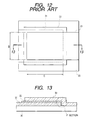
- Fig. 12 is a plan of a conventionally known thin-film capacitor element, and Fig. 13, a sectional view along line 13-13 in Fig. 12.
- a conventional thin-film capacitor element consists of a stacked structure of a lower electrode 31, a dielectric layer 32 and an upper electrode 33 formed over a substrate 30, and the capacitance of the capacitor is determined by the range in which the lower electrode 31 and the upper electrode 33 overlap each other.
- the lower electrode 31 is formed of Cu or the like sputtered or plated over the substrate 30 and etched into a desired pattern shape.
- the dielectric layer 32 is formed of SiO 2 or the like sputtered or chemical vapor-deposited over the lower electrode 31 and the substrate 30 and etched into a desired pattern shape.
- the patterned dielectric layer 32 extends to over the substrate 30 via the top face and side faces of the lower electrode 31.
- the upper electrode 33 is formed of Cu or the like sputtered or plated over the dielectric layer 32 and the substrate 30 and etched into a desired pattern shape.
- the patterned upper electrode 33 extends to over the substrate 30 via the top face and side faces of the dielectric layer 32.
- one of the requirements for such a thin-film capacitor element concerns the breakdown voltage between the lower electrode 31 and the upper electrode 33. If this breakdown voltage is below the required level, the thin-film capacitor element will be broken down at a low voltage and can no longer operate as such.
- the breakdown voltage is heavily dependent on the thickness of the dielectric layer 32 intervening between the two electrodes 31 and 33. Increasing the thickness of the dielectric layer 32 would raise the breakdown voltage, but in the conventional thin-film capacitor element described above the dielectric layer 32 becomes thinner near the corners of the lower electrode 31 (see section P in Fig. 13) and thereby invites a drop of the breakdown voltage.
- the dielectric layer 32 can be improved by thinning the lower electrode 31 to reduce the level gap, the thinner the lower electrode 31 and the upper electrode 33, the greater the resistance component of conductors in series, which would give rise to another problem of an lowered Q value of the thin-film capacitor element. Or if the overall thickness of the dielectric layer 32 is increased, the breakdown voltage can be prevented from dropping, but the thicker the dielectric layer 32, the smaller its capacitance per unit square measure. Accordingly, the thin-film capacitor element will become bigger and, moreover, as a greater thickness of the dielectric layer 32 does not serve to stabilize the shape of coverage, fluctuations of the breakdown voltage will remain.
- the capacitance of the capacitor is determined by the range in which the lower electrode 31 and the upper electrode 33 overlap each other (the rectangle of B ⁇ C in Fig. 12).
- the size and alignment of the two electrodes 31 and 33 tend to be adversely affected in accuracy by fluctuations in side etching quantity and etch rate, giving rise to a problem of fluctuations in the capacitance of the capacitor element.
- This problem is more serious with thin-film capacitor elements of smaller capacitances, because a smaller capacitance means a smaller area of overlap between the lower electrode 31 and the upper electrode 33 and accordingly the impact of accuracy fluctuations of etching and overlapping on the capacitance increases in relative terms.
- an alumina substrate used in this kind of electronic circuit board has the aforementioned advantages, at the same time it is inferior in surface smoothness to sapphire and other monocrystalline substrates.
- the surface roughness (Ra) of an alumina substrate of 99.5% in purity, for instance, is 30 to 100 nm in terms of unevenness.
- a lower electrode and a dielectric layer are successively stacked over a substrate, the periphery of this dielectric layer is covered with an insulating layer having an opening, and an upper electrode formed over this insulating layer is stacked over the dielectric layer within the opening.
- This configuration which ensures insulation between the lower electrode and the upper electrode by the insulating layer covering the dielectric layer, can securely prevent any drop or fluctuation of the breakdown voltage due to inadequate coverage of the dielectric layer. Furthermore, as the opening in the insulating layer determines the capacitance of the capacitor, fluctuations in capacitance can be reduced irrespective of the accuracy of the lower electrode and the upper electrode in size and alignment.
- the insulating layer of a photosensitive resist it is preferable to form the insulating layer of a photosensitive resist.
- the formation of the insulating layer of a photosensitive resist makes possible highly accurate formation of the opening and more effective reduction of capacitance fluctuations.
- the dielectric layer at least over the surface of the lower electrode, it is possible to form the dielectric layer continuously from the top and side faces of the lower electrode to the substrate, and in this case, as the lower electrode and the upper electrode are insulated by two layers , i.e. the dielectric layer and the insulating layer , even if the coverage of the dielectric layer is inadequate in the level gap of the lower electrode, any drop or fluctuation of the breakdown voltage can be securely prevented in spite of this inadequate coverage.
- the dielectric layer only over the surface of the lower electrode and part of the insulating layer from the periphery of the dielectric layer to over the substrate .
- insulation between the lower electrode and the upper electrode is accomplished by the insulating layer alone, the formation of part of the insulating layer directly over the substrate can enhance the tightness of the adhesion of the insulating layer.
- an insulating layer is formed over part of an alumina substrate, and a capacitor element consisting of a lower electrode, a dielectric layer and an upper electrode stacked successively is formed over this insulating layer, and at least an inductor element and a transmission line are formed, each in a filmy state, over the alumina substrate.
- the breakdown voltage of the capacitor element formed in a filmy state over the insulating can be prevented from dropping. Furthermore, as the insulating film which suffers a great dielectric loss does not adversely affect the inductor element and the transmission line, the high frequency performance can be prevented from deteriorating.
- the lower electrode and upper electrode of the capacitor element it is preferable for the lower electrode and upper electrode of the capacitor element to overlap each other within the contour of the insulating layer, and this disposition can securely prevent the breakdown voltage of the capacitor element from dropping.
- circuit elements in the foregoing configuration are to include a resistance element besides a capacitor element and an inductor element, especially where a material having a relatively high specific resistance, such as TaSiO 2 , is used as the resistance layer of the resistance element, it is preferable from the viewpoint of preventing deterioration of the high frequency performance to form in a filmy state this resistance layer over the surface of the alumina substrate like the inductor element and the transmission line.
- a material having a relatively low specific resistance such as Ta 2 N
- the resistance of the resistance element formed in a filmy state over the insulating layer can be prevented from fluctuating substantially, because fine ups and downs of the alumina substrate are smoothened by the insulating layer.
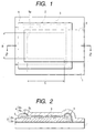
- Fig. 1 shows a plan of the first preferred embodiment of the invention
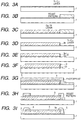
- Fig. 2 shows a section along line 2-2 in Fig. 1
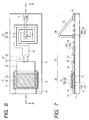
- Figs. 3 and 4 illustrate a production process of this thin-film capacitor element.
- the thin-film capacitor element embodying the invention in this mode is configured of a lower electrode 2, a dielectric layer 3, an upper electrode 4 and an insulating layer 5 arranged to intervene between the periphery of the insulating layer 5 and the upper electrode 4, wherein the upper electrode 4 is stacked over the dielectric layer 3 within an opening 5a formed in the insulating layer 5.
- the substrate 1 is made of alumina (of 99.5% in purity for instance) , over which the lower electrode 2 is formed of a thin film by sputtering or plating.
- the lower electrode 2 consists of a first lower electrode layer 2a and a second lower electrode layer 2b, and its overall thickness is set in a range of 0.5 to 5 ⁇ m with a view to achieve a high Q value.
- the first lower electrode layer 2a is formed by sputtering Ti/Cu, for instance, on the substrate 1 and etching it into a desired pattern shape, while the second lower electrode layer 2b is formed by plating the surface of the first lower electrode layer 2a with Cu/Ni for example.
- the dielectric layer 3 Over the lower electrode 2 is formed the dielectric layer 3 in a filmy state.
- This dielectric layer 3 is formed by sputtering or chemically vapor-depositing SiO 2 , for instance, over the second lower electrode layer 2b and the substrate 1 and etching it into a desired pattern shape.
- the patterned dielectric layer 3 extends to over the substrate 1 via the top face and side faces of the lower electrode 2. In this case, as the dielectric layer 3 is formed in the level gap part of the lower electrode 2 (the first lower electrode layer 2a and the second lower electrode layer 2b), the coverage of the dielectric layer 3 is inadequate in that part.
- the periphery of the dielectric layer 3, including this part of inadequate coverage, is covered by the insulating layer 5, and the rest of the dielectric layer 3 is positioned within the rectangular opening 5a formed in the insulating layer 5.
- This insulating layer 5 is formed by spin-coating the dielectric layer 3 all over from above with a positive type photoresist, for example, and exposing to light and developing the photoresist into a desired pattern.
- the opening 5a is formed in the patterned insulating layer 5.
- the upper electrode 4 of a thin film by sputtering or plating, and the upper electrode 4 is stacked over the dielectric layer 3 within the opening 5a.
- This upper electrode 4 consists of a first upper electrode layer 4a and a second upper electrode layer 4b, and its overall thickness is set in a range of 0.5 to 5 ⁇ m with a view to achieve a high Q value.
- the first upper electrode layer 4a is formed by sputtering Ti/Cu, for instance, all over the insulating layer 5 and etching it into a desired pattern shape, while the second upper electrode layer 4b is formed by plating the surface of the first upper electrode layer 4a with Cu/Ni for example.
- a positive type photoresist (a product of Clariant: AZ-P4620) over this Ti/Cu layer. Exposure to light and development of this photoresist results in a resist pattern of a desired shape as shown in Fig. 3B.
- a positive type photoresist a product of Clariant: AZ-P4620
- films of Cu (3 ⁇ m) and Ni (0.3 ⁇ m) are electroplated successively to form a Cu/Ni layer over the Ti/Cu layer, followed by the formation of the second lower electrode layer 2b by peeling off the resist pattern as shown in Fig. 3D.
- the lower electrode 2 consisting of the first lower electrode layer 2a and the second lower electrode layer 2b is formed over the substrate 1 as illustrated in Fig. 3E.
- an SiO 2 (0.3 ⁇ m) film is sputtered over the second lower electrode layer 2b and the substrate 1 including the level gap part of the lower electrode 2, and this SiO 2 film is etched using a positive type photoresist (a product of Tokyo Ohka Kogyo: OFPR-7450) to form the dielectric layer 3 continuously to the substrate 1 via the top and side faces of the lower electrode 2 as illustrated in Fig. 3F.
- a positive type photoresist a product of Tokyo Ohka Kogyo: OFPR-7450
- the footrest is patterned to a desired shape by exposure to light and development as shown in Fig. 3H, followed by curing (at 240 °C for 60 minutes).
- a positive type photoresist a product of Clariant: AZ-P4620
- the footrest is patterned to a desired shape by exposure to light and development as shown in Fig. 3H, followed by curing (at 240 °C for 60 minutes).
- the result is the insulating layer 5 having the opening 5a as shown in Fig. 3I.
- the pattern shape of the insulating layer 5 in this case is dependent on the precision of masking during the exposure of the photoresist, the opening 5a can be formed highly accurately.
- the end face of the lower electrode 2 (level gap part) is covered with two layers, i.e. the dielectric layer 3 and the insulating layer 5.
- a positive type photoresist (a product of Clariant: AZ-P4620) over this Ti/Cu layer. Exposure to light and development of this photoresist results in a resist pattern of a desired shape as shown in Fig. 4B. Then, as illustrated in Fig.
- films of Cu (3 ⁇ m) and Ni (0.3 ⁇ m) are electroplated successively to form a Cu/Ni layer over the Ti/Cu layer, followed by the formation of the second upper electrode layer 4b by peeling off the resist pattern as shown in Fig. 4D.
- the upper electrode 4 consisting of the first upper electrode layer 4a and the second upper electrode layer 4b is formed as shown in Fig. 4E to provide the thin-film capacitor element illustrated in Figs. 1 and 2.
- the thin-film capacitor element which is the first preferred embodiment of the invention
- the insulating layer 5 covering the periphery of the dielectric layer 3 any drop or fluctuation of the breakdown voltage can be prevented without fail in spite of this inadequate coverage of the dielectric layer 3. Therefore, it is made possible to achieve a high Q value by increasing the thicknesses of the lower electrode 2 and the upper electrode 4 and at the same time to make the shape of the thin-film capacitor element smaller by reducing the thickness of the dielectric layer 3.
- the capacitance of the capacitor is determined by the opening 5a of the insulating layer 5 (the rectangle of B ⁇ C in Fig.
- any fluctuations in capacitance can be reduced irrespective of any adverse effects on the upper electrode 2 and the lower electrode 4 in size or alignment accuracy by fluctuations in side etching quantity and etch rate.
- the opening 5a of the insulating layer 5 can be formed with high precision, making it possible to reduce fluctuations in capacitance even more effectively.
- Fig. 5 shows a section of a thin-film capacitor element, which is a second preferred embodiment of the invention.
- This thin-film capacitor element differs from the above-described first embodiment in that the dielectric layer 3 is formed only over the surface of the lower electrode 2, and part of the insulating layer 5 covering the periphery of this dielectric layer 3 is extended to above the substrate 1.
- the two embodiments are basically the same in all the other aspects of configuration.
- the insulating layer 5 ensures insulation between the lower electrode 2 and the upper electrode 4, resulting in a similar effect to that of the above-described first embodiment. Moreover, as part of the insulating layer 5 can be formed directly over the substrate 1, the adhesion between the insulating layer 5 and the substrate 1 can be made even tighter.
- the lower electrode 2 is formed directly over the substrate 1 in both of the embodiments described above, the surface of the substrate 1 may as well be coated with an insulating layer to have this insulating layer formed between the lower electrode 2 and the substrate 1.
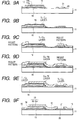
- Figs. 6 and 7 illustrate the electronic circuit board in which circuit elements including a capacitor element 12, a resistance element 13 and an inductor element 14 and transmission lines linking these circuit elements are formed each in a filmy state over an alumina substrate 11. Many of these circuit elements 12, 13 and 14 and transmission lines 15 are formed in the effective area of the alumina substrate 11 according to the requirements of each particular circuit configuration, and Figs. 6 and 7 illustrate only part of them.
- the surface roughness (Ra) of the alumina substrate 11 has ups and downs of about 30 to 100 nm, and this unevenness is due to the porous sintered material of the alumina substrate 11 and the resultant existence of many fine dents in its surface.
- an insulating layer 16 Over part of the alumina substrate 11 is formed an insulating layer 16, and the filling of the many fine dents in the surface of the alumina substrate 11 with this insulating layer 16 serves to reduce the surface roughness (Ra) of the insulating layer 16 to 10 nm or less.
- the insulating layer 16, consisting of a positive type photosensitive high molecular film such as a photoresist, is formed by exposing to light and developing the film to a desired pattern shape using a mask.
- the capacitor element 12 is configured of a lower electrode 17, a dielectric layer 18 and an upper electrode 19 successively stacked over the insulating layer 16, within which the lower electrode 17 and the upper electrode 19 are caused to overlap each other within the insulating layer 16 to serve as the effective area of the capacitor.
- the contour of the insulating layer 16 proves too large for the effective area of the capacitor, the two-dimensional proportion of the insulating layer 16 in the limited space over the alumina substrate 11 will increase, resulting in a contraction of the effective area for circuit elements that can be formed over the alumina substrate 11 and accordingly in a reduced area efficiency.
- the contour of the insulating layer 16 is set to be 10 to 100 ⁇ m greater than the designed value of the effective area of the capacitor.
- the lower electrode 17 is a double structure of a first lower electrode layer 17a and a second lower electrode layer 17b, and its total thickness is set within the range of 0.5 to 5 ⁇ m with a view to achieving a high Q value.
- the first lower electrode layer 17a consists of a metallic film of Ti/Cu or the like formed in a filmy state by sputtering over the insulating layer 16
- the second lower electrode layer 17b consists of a metallic film of Cu/Ni or the like formed in a filmy state by plating over the first lower electrode layer 17a.
- the upper electrode 19 also is a double structure of a first upper electrode layer 19a and a second upper electrode layer 19b, and its total thickness is set within the range of 0.5 to 5 ⁇ m with a view to achieving a high Q value.
- the first upper electrode layer 19a consists of a metallic film of Ti/Cu or the like formed in a filmy state by sputtering over the dielectric layer 18, and the second upper electrode layer 19b consists of a metallic film of Cu/Ni or the like formed in a filmy state by plating over the first upper electrode layer 19a.
- the resistance element 13 consists of a resistance layer 20 and an insulation protective layer 21 successively stacked over the alumina substrate 11, and both ends of the resistance layer 20 are connected to the transmission line 15.
- the resistance layer 20 consists of a resistant material having a relatively high specific resistance, such as TaSiO 2 , and is formed in a filmy state by sputtering over the alumina substrate 11.
- the inductor element 14 is configured of a conductor film 22 formed in a filmy state over the alumina substrate 11 and a bonding wire 23 connecting its two ends, which are connected to the transmission line 15.
- the conductor film 22, formed in a rectangular spiral shape, is a double structure of a first conductor layer 22a and a second conductor layer 22b.
- the transmission line 15, too, is a double structure of a first conductor layer 15a and a second conductor layer 15b, and these conductor film 22 and transmission line 15 consist of respectively the same materials as the above-described lower electrode 17 and upper electrode 19 of the capacitor element 12.
- the first conductor layers 15a and 22a consist of a metallic film of Ti/Cu or the like formed in a filmy state by sputtering over the alumina substrate 11
- the second conductor layers 15b and 22b consist of a metallic film of Cu/Ni or the like formed in a filmy state by plating over the first upper conductor layers 15a and 22a.
- a film of TaSiO 2 is formed by sputtering over the alumina substrate 11, and a rectangular resistance layer 20 is formed over the alumina substrate 11 as shown in Fig. 8A by etching the film by RIE after patterning a photoresist.
- TaSiO 2 is a resistant material having a relatively high specific resistance, a desired level of resistance can be achieved even if the resistance layer 20 is made thick enough, and the formation of the resistance layer 20 directly over the alumina substrate 11 would not invite substantial fluctuations in resistance due to fine ups and downs of the surface of the alumina substrate 11.
- the alumina substrate 11 is spin-coated all over with a positive type photoresist (a product of Clariant: AZ-P4620) and, after patterning it into a desired shape by exposure to light and development using a mask, it is subjected to curing (at 240 °C for 60 minutes) to form the insulating layer 16 in a prescribed position on the alumina substrate 11 as shown in Fig. 8B.
- the insulation protective layer 21 is formed over the resistance layer 20.
- an SiO 2 layer (0.3 ⁇ m) by sputtering and, by etching this SiO 2 layer by RIE after the patterning of a positive type photoresist (a product of Tokyo Ohka Kogyo: OFPR-7450), the dielectric layer 18 continuous from the top and side faces of the lower electrode 17 and the alumina substrate 11 is formed as illustrated in Fig. 9A.
- Fig. 9B from above the dielectric layer 18 and the insulation protective layer 21 films of Ti (0.1 ⁇ m) and Cu (0.1 ⁇ m) are successively sputtered to form a Ti/Cu layer, followed by spin coating of a positive type photoresist (a product of Clariant: AZ-P4620) over this Ti/Cu layer, and this photoresist is exposed to light and developed to form a resist pattern of a desired pattern as shown in Fig. 9C. Further, as illustrated in Fig. 9D, films of Cu (3 ⁇ m) and Ni (0.3 ⁇ m) are successively formed over the Ti/Cu layer by electroplating to form a Cu/Ni layer, followed by peeling off the resist pattern as shown in Fig. 9E.
- a positive type photoresist a product of Clariant: AZ-P4620
- the upper electrode 19 consisting of the first upper electrode layer 19a and the second upper electrode layer 19b is formed as shown in Fig. 9F, and at the same time the transmission line 15 (the first conductor layer 15a and the second conductor layer 15b), which is the guiding pattern of this upper electrode 19 and the resistance layer 20, is also formed.
- the conductor film 22 of this inductor element 13 can be formed at the same steps as the upper electrode 19 and the transmission line 15.
- the conductor film 22 of the inductor element 13 consisting of the first conductor layer 22a and the second conductor layer 22b, can be formed over the alumina substrate 11 by patterning the Ti/Cu layer and the Cu/Ni layer in a desired pattern, using a resist pattern or the like, at the steps shown in Figs. 9B through 9F. Therefore, after forming in a filmy state these circuit elements 12 through 14 and the transmission line 15 over the alumina substrate 11, connecting the bonding wire 23 to the conductor film 22 of the inductor element 13 can give the electronic circuit board illustrated in Figs. 6 and 7.
- the insulating layer 16 formed over part of the alumina substrate 11 smoothens fine ups and downs of the surface of the alumina substrate 11, and the capacitor element 12 consisting of the lower electrode 17, the dielectric layer 18 and the upper electrode 19 successively stacked over this insulating layer 16 is formed in a filmy state.
- the dielectric layer 18 can be formed in a uniform thickness over the lower electrode 17, and the breakdown voltage of the capacitor element 12 can be thereby prevented from dropping.
- the conductor film 22 of the inductor element 14 and the transmission line 15 are formed in a filmy state over the surface of the alumina substrate 11 where the insulating layer 16 is not formed, the insulating layer 16, whose dielectric loss is significant, does not adversely affect these resistance element 13, inductor element 14 and transmission line 15, and the high frequency performance can be thereby prevented from deterioration.
- Fig. 10 shows a plan of an essential part of an electronic circuit board, which is another preferred embodiment of the invention
- Fig. 11 shows a section along line 11-11 in Fig. 10.
- parts having their counterparts in Figs . 6 and 7 are assigned respectively the same reference signs.
- the resistance layer 20 of the resistance element 13 consists of a material having a relatively low specific resistance, such as Ta 2 N, and another insulating layer 16 is also formed underneath this resistance layer 20.
- the lower electrode 17 of the capacitor element 12 and the resistance layer 20 of the resistance element 13 are formed in a filmy state over the insulating layer 16 which is partially formed over the alumina substrate 11, and other elements, i.e. the inductor element 14 and the transmission line 15, are formed in a filmy state over the alumina substrate 11.
- the resistance layer 20 of the resistance element 13 consists of a material having a relatively low specific resistance, such as Ta 2 N.
- the insulation protective layer 21 to cover the surface of the resistance layer 20 needs to be formed in a separate process from the insulating layer 16.
- the capacitor element 12 and the resistance element 13 are formed in a filmy state over the insulating layer 16 partially formed over the surface of the alumina substrate 11, it is possible to prevent the breakdown voltage of the capacitor element 12 from dropping. Moreover, in spite of the use of a material having a relatively low specific resistance, such as Ta 2 N, for the resistance layer 20 of the resistance element 13, the level of resistance can be prevented from fluctuating. Also, though the high frequency performance is somewhat deteriorated by the insulating layer 16 underneath the resistance element 13, the high frequency performance can be prevented from significant deterioration because other elements , i.e. the inductor element 14 and the transmission line 15, are formed in a filmy state over the alumina substrate 11 and accordingly the insulating layer 16, whose dielectric loss is significant, does not adversely affect the inductor element 14 and the transmission line 15.
- the insulating layer 16 is partially formed over the alumina substrate 11 by exposing to light and developing a positive type photosensitive high molecular film such as a photoresist, it is also possible to coat the whole surface of the alumina substrate 11 with a glass film and patterning this film in a desired shape to form the insulating layer 16.
- an insulating layer is partially formed over the surface of the alumina substrate; a capacitor element consisting of a lower electrode, a dielectric layer and an upper electrode successively stacked is formed in a filmy state over this insulating layer; and at least an inductor element and a transmission line are formed over the surface of the alumina substrate, each in a filmy state.
Landscapes
- Engineering & Computer Science (AREA)
- Microelectronics & Electronic Packaging (AREA)
- Fixed Capacitors And Capacitor Manufacturing Machines (AREA)
- Parts Printed On Printed Circuit Boards (AREA)
- Semiconductor Integrated Circuits (AREA)
Abstract
Description
Claims (9)
- A thin-film capacitor element wherein a lower electrode and a dielectric layer are successively stacked over a substrate, the periphery of this dielectric layer is covered with an insulating layer having an opening, and an upper electrode formed over this insulating layer is stacked over the dielectric layer within the opening.
- The thin-film capacitor element, according to Claim 1, wherein the insulating layer is formed of a photosensitive resist.
- The thin-film capacitor element, according to Claim 1 or 2, wherein the dielectric layer is formed continuously from the top and side faces of the lower electrode to the substrate.
- The thin-film capacitor element, according to Claim 2, wherein the dielectric layer is formed only over the surface of the lower electrode, and part of the insulating layer is formed from the periphery of the dielectric layer to the substrate.
- An electronic circuit board substrate wherein an insulating layer is formed over part of a substrate, and a capacitor element consisting of a lower electrode, a dielectric layer and an upper electrode stacked successively is formed over this insulating layer, and at least an inductor element and a transmission line are formed, each in a filmy state, over the substrate.
- The electronic circuit board, according to Claim 5, wherein the lower electrode and upper electrode overlap each other within the contour of the insulating layer.
- The electronic circuit board, according to Claim 6, wherein the insulating layer consists of a photosensitive high molecular film.
- The electronic circuit board, according to Claim 7, wherein a resistance element is further formed in a filmy state over the surface of the substrate.
- The electronic circuit board, according to Claim 8, wherein the resistance element consists of Ta2N.
Applications Claiming Priority (4)
| Application Number | Priority Date | Filing Date | Title |
|---|---|---|---|
| JP2000202394 | 2000-07-04 | ||
| JP2000202394A JP2002025854A (en) | 2000-07-04 | 2000-07-04 | Thin-film capacitor |
| JP2000216223 | 2000-07-17 | ||
| JP2000216223A JP3759381B2 (en) | 2000-07-17 | 2000-07-17 | Electronic circuit board |
Publications (2)
| Publication Number | Publication Date |
|---|---|
| EP1170797A2 true EP1170797A2 (en) | 2002-01-09 |
| EP1170797A3 EP1170797A3 (en) | 2005-05-25 |
Family
ID=26595357
Family Applications (1)
| Application Number | Title | Priority Date | Filing Date |
|---|---|---|---|
| EP01305412A Withdrawn EP1170797A3 (en) | 2000-07-04 | 2001-06-22 | Thin-film capacitor element and electronic circuit board on which thin-film capacitor element is formed |
Country Status (2)
| Country | Link |
|---|---|
| US (1) | US6552384B2 (en) |
| EP (1) | EP1170797A3 (en) |
Cited By (6)
| Publication number | Priority date | Publication date | Assignee | Title |
|---|---|---|---|---|
| EP1416526A3 (en) * | 2002-10-30 | 2007-02-21 | Fujitsu Limited | Semiconducteur device and manufacturing method of a semiconductor device |
| WO2009071142A3 (en) * | 2007-12-05 | 2009-11-26 | Rohde & Schwarz Gmbh & Co. Kg | Electrical circuit arrangement and filter having concentrated elements comprising said electrical circuit arrangement in multi-layer substrates |
| CN109585161A (en) * | 2017-09-29 | 2019-04-05 | 日月光半导体制造股份有限公司 | Capacitor arrangement |
| CN112530939A (en) * | 2020-11-19 | 2021-03-19 | 偲百创(深圳)科技有限公司 | Integrated capacitor, manufacturing method thereof and radio frequency circuit |
| EP3849286A1 (en) * | 2020-01-09 | 2021-07-14 | Murata Manufacturing Co., Ltd. | Electronic device with differential transmission lines equipped with 3d capacitors supported by a base, and corresponding manufacturing method |
| EP4163941A4 (en) * | 2020-06-04 | 2024-01-10 | Toppan Inc. | MULTILAYER WIRING BOARD AND MODULE COMPRISING A MULTILAYER WIRING BOARD |
Families Citing this family (16)
| Publication number | Priority date | Publication date | Assignee | Title |
|---|---|---|---|---|
| US20020171530A1 (en) * | 2000-03-30 | 2002-11-21 | Victor Company Of Japan, Limited | Production method of thin film passive element formed on printed circuit board and thin film passive element produced by the method |
| UA77459C2 (en) * | 2001-11-03 | 2006-12-15 | Thin-film capacitor and a method for producing the capacitor | |
| JP2003234410A (en) * | 2002-02-08 | 2003-08-22 | Fujitsu Ltd | Capacitor, method of manufacturing the same, and semiconductor device |
| JP3886413B2 (en) * | 2002-05-17 | 2007-02-28 | Necエレクトロニクス株式会社 | Semiconductor device and manufacturing method thereof |
| CN100341059C (en) * | 2002-12-19 | 2007-10-03 | 富士胶片株式会社 | Optical information recording method and optical information recording medium |
| JPWO2005036939A1 (en) * | 2003-10-07 | 2006-12-28 | 株式会社Neomaxマテリアル | Substrate and manufacturing method thereof |
| JP3997979B2 (en) * | 2003-10-24 | 2007-10-24 | セイコーエプソン株式会社 | Electro-optical device substrate manufacturing method and electro-optical device substrate, electro-optical device and electronic device, semiconductor device substrate manufacturing method, and semiconductor device substrate |
| US7239194B2 (en) * | 2004-03-25 | 2007-07-03 | Integral Wave Technologies, Inc. | Trench capacitor power supply system and method |
| JP4684856B2 (en) * | 2005-11-08 | 2011-05-18 | 富士通株式会社 | Electronic components |
| JP2007142109A (en) * | 2005-11-17 | 2007-06-07 | Tdk Corp | Electronic components |
| JP4518013B2 (en) * | 2005-12-14 | 2010-08-04 | Tdk株式会社 | Electronic components |
| JP2007300002A (en) * | 2006-05-01 | 2007-11-15 | Tdk Corp | Electronic components |
| US8497449B1 (en) * | 2006-05-26 | 2013-07-30 | Synchron Laser Service Inc. | Micro-machining of ceramics using an ytterbium fiber-laser |
| KR20100041179A (en) * | 2008-10-13 | 2010-04-22 | 매그나칩 반도체 유한회사 | Insulator, capacitor with the same and fabricating method thereof, and method for fabricating semiconductor device |
| IT1392793B1 (en) * | 2008-12-30 | 2012-03-23 | St Microelectronics Srl | INTEGRATED CONDENSER WITH NON-UNIFORM THICKNESS PLATE |
| WO2018117111A1 (en) | 2016-12-21 | 2018-06-28 | 大日本印刷株式会社 | Through electrode substrate, semiconductor device and method for producing through electrode substrate |
Family Cites Families (13)
| Publication number | Priority date | Publication date | Assignee | Title |
|---|---|---|---|---|
| JPS5637692A (en) * | 1979-09-04 | 1981-04-11 | Nippon Electric Co | Method of manufacturing hybrid thin film integrated circuit board |
| US4490457A (en) * | 1980-11-28 | 1984-12-25 | Honeywell Inc. | Cold/dry substrate treatment technique which improves photolithographic limits of resolution and exposure tolerance |
| JPS583258A (en) * | 1981-06-30 | 1983-01-10 | Toshiba Corp | Semiconductor device |
| US4980555A (en) * | 1988-10-31 | 1990-12-25 | Honeywell Inc. | Electrical interconnector for infrared detector arrays |
| JPH02263445A (en) * | 1988-12-23 | 1990-10-26 | Toshiba Corp | Aluminum nitride substrate and semiconductor using same |
| JPH0574654A (en) * | 1991-09-13 | 1993-03-26 | Matsushita Electric Ind Co Ltd | Organic thin film capacitor |
| JP3253756B2 (en) * | 1993-05-13 | 2002-02-04 | 島田理化工業株式会社 | Thin film capacitor and method of manufacturing the same |
| JP2586797B2 (en) * | 1993-09-03 | 1997-03-05 | 日本電気株式会社 | Manufacturing method of printed wiring board |
| JPH08148795A (en) * | 1994-11-18 | 1996-06-07 | Matsushita Electric Ind Co Ltd | Thin film circuit board |
| JPH09312457A (en) * | 1996-05-23 | 1997-12-02 | Kyocera Corp | Circuit board with capacitive element |
| JPH09321166A (en) * | 1996-05-28 | 1997-12-12 | Ngk Spark Plug Co Ltd | Method for manufacturing hybrid integrated circuit board |
| JPH1022457A (en) * | 1996-07-03 | 1998-01-23 | Mitsubishi Electric Corp | Capacitance device, semiconductor device, and manufacturing method thereof |
| TW386289B (en) * | 1997-07-03 | 2000-04-01 | Matsushita Electronics Corp | Capacitance element and manufacturing thereof |
-
2001
- 2001-06-22 EP EP01305412A patent/EP1170797A3/en not_active Withdrawn
- 2001-07-02 US US09/898,670 patent/US6552384B2/en not_active Expired - Fee Related
Cited By (16)
| Publication number | Priority date | Publication date | Assignee | Title |
|---|---|---|---|---|
| EP1416526A3 (en) * | 2002-10-30 | 2007-02-21 | Fujitsu Limited | Semiconducteur device and manufacturing method of a semiconductor device |
| US7547933B2 (en) | 2002-10-30 | 2009-06-16 | Fujitsu Microelectronics Limited | Semiconductor device and manufacturing method of a semiconductor device |
| US8153448B2 (en) | 2002-10-30 | 2012-04-10 | Fujitsu Semiconductor Limited | Manufacturing method of a semiconductor device |
| US8652854B2 (en) | 2002-10-30 | 2014-02-18 | Fujitsu Semiconductor Limited | Manufacturing method of a semiconductor device |
| WO2009071142A3 (en) * | 2007-12-05 | 2009-11-26 | Rohde & Schwarz Gmbh & Co. Kg | Electrical circuit arrangement and filter having concentrated elements comprising said electrical circuit arrangement in multi-layer substrates |
| US8681474B2 (en) | 2007-12-05 | 2014-03-25 | Rohde & Schwartz Gmbh & Co. Kg | Electrical circuit arrangement with concentrated elements in multi-layer substrates |
| US8860531B2 (en) | 2007-12-05 | 2014-10-14 | Rohde & Schwarz Gmbh & Co. Kg | Filter having electrical circuit arrangement with concentrated elements in multi-layer substrates |
| CN109585161A (en) * | 2017-09-29 | 2019-04-05 | 日月光半导体制造股份有限公司 | Capacitor arrangement |
| TWI890725B (en) * | 2020-01-09 | 2025-07-21 | 日商村田製作所股份有限公司 | Electronic device with differential transmission lines equipped with capacitors supported by a base, and corresponding manufacturing method |
| EP3849286A1 (en) * | 2020-01-09 | 2021-07-14 | Murata Manufacturing Co., Ltd. | Electronic device with differential transmission lines equipped with 3d capacitors supported by a base, and corresponding manufacturing method |
| WO2021140477A1 (en) * | 2020-01-09 | 2021-07-15 | Murata Manufacturing Co., Ltd. | Electronic device with differential transmission lines equipped with capacitors supported by a base, and corresponding manufacturing method |
| US12260996B2 (en) | 2020-01-09 | 2025-03-25 | Murata Manufacturing Co., Ltd. | Electronic device with differential transmission lines equipped with capacitors supported by a base, and corresponding manufacturing method |
| EP4163941A4 (en) * | 2020-06-04 | 2024-01-10 | Toppan Inc. | MULTILAYER WIRING BOARD AND MODULE COMPRISING A MULTILAYER WIRING BOARD |
| US12456697B2 (en) | 2020-06-04 | 2025-10-28 | Toppan Inc. | Multilayer wiring substrate and module having multilayer wiring substrate |
| CN112530939B (en) * | 2020-11-19 | 2023-11-07 | 偲百创(深圳)科技有限公司 | Integrated capacitor and manufacturing method thereof, radio frequency circuit |
| CN112530939A (en) * | 2020-11-19 | 2021-03-19 | 偲百创(深圳)科技有限公司 | Integrated capacitor, manufacturing method thereof and radio frequency circuit |
Also Published As
| Publication number | Publication date |
|---|---|
| US6552384B2 (en) | 2003-04-22 |
| US20020003261A1 (en) | 2002-01-10 |
| EP1170797A3 (en) | 2005-05-25 |
Similar Documents
| Publication | Publication Date | Title |
|---|---|---|
| US6552384B2 (en) | Thin-film capacitor element and electronic circuit board on which thin-film capacitor element is formed | |
| US7079371B2 (en) | Capacitor device, electronic parts packaging structure, and method of manufacturing the capacitor device | |
| US20220028602A1 (en) | Inductor component | |
| US7453343B2 (en) | Thin-film type common-mode choke coil | |
| US6678144B2 (en) | Capacitor, circuit board with built-in capacitor and method for producing the same | |
| US20090000093A1 (en) | Capacitor and method of manufacturing the same and capacitor unit | |
| JP7159997B2 (en) | inductor components | |
| SE520173C2 (en) | Process for manufacturing a capacitor in an integrated circuit | |
| CN115036110B (en) | Inductor components | |
| US4890192A (en) | Thin film capacitor | |
| US20240379650A1 (en) | Filter and manufacturing method therefor | |
| JP5023999B2 (en) | Thin film capacitor and manufacturing method thereof | |
| US6830984B2 (en) | Thick traces from multiple damascene layers | |
| JP2003017366A (en) | Thin film capacitor element and its manufacturing method | |
| JP2002025854A (en) | Thin-film capacitor | |
| JP3765366B2 (en) | Planar magnetic element integrated semiconductor device | |
| JP2002033559A (en) | Electronic circuit board | |
| JPH09199365A (en) | High frequency inductor manufacturing method | |
| RU2046429C1 (en) | Film capacitor | |
| JP2002280219A (en) | Inductor and / or circuit wiring near the inductor and method for manufacturing the same | |
| CN115458275A (en) | Inductor and preparation method thereof, and filter | |
| JP2002033560A (en) | Manufacturing method for electronic circuit board | |
| US20250008662A1 (en) | Functional substrate and method for manufacturing the same, and electronic device | |
| US12374485B2 (en) | Inductor component | |
| WO2023245593A1 (en) | Filter and manufacturing method therefor |
Legal Events
| Date | Code | Title | Description |
|---|---|---|---|
| PUAI | Public reference made under article 153(3) epc to a published international application that has entered the european phase |
Free format text: ORIGINAL CODE: 0009012 |
|
| AK | Designated contracting states |
Kind code of ref document: A2 Designated state(s): AT BE CH CY DE DK ES FI FR GB GR IE IT LI LU MC NL PT SE TR |
|
| AX | Request for extension of the european patent |
Free format text: AL;LT;LV;MK;RO;SI |
|
| PUAL | Search report despatched |
Free format text: ORIGINAL CODE: 0009013 |
|
| AK | Designated contracting states |
Kind code of ref document: A3 Designated state(s): AT BE CH CY DE DK ES FI FR GB GR IE IT LI LU MC NL PT SE TR |
|
| AX | Request for extension of the european patent |
Extension state: AL LT LV MK RO SI |
|
| 17P | Request for examination filed |
Effective date: 20050527 |
|
| AKX | Designation fees paid |
Designated state(s): DE FR GB |
|
| STAA | Information on the status of an ep patent application or granted ep patent |
Free format text: STATUS: THE APPLICATION IS DEEMED TO BE WITHDRAWN |
|
| 18D | Application deemed to be withdrawn |
Effective date: 20060303 |