EP1168439A2 - Goldverbindungsdraht für ein Halbleiterbauelement - Google Patents
Goldverbindungsdraht für ein Halbleiterbauelement Download PDFInfo
- Publication number
- EP1168439A2 EP1168439A2 EP01250061A EP01250061A EP1168439A2 EP 1168439 A2 EP1168439 A2 EP 1168439A2 EP 01250061 A EP01250061 A EP 01250061A EP 01250061 A EP01250061 A EP 01250061A EP 1168439 A2 EP1168439 A2 EP 1168439A2
- Authority
- EP
- European Patent Office
- Prior art keywords
- ppm
- mass
- wire
- bonding
- gold
- Prior art date
- Legal status (The legal status is an assumption and is not a legal conclusion. Google has not performed a legal analysis and makes no representation as to the accuracy of the status listed.)
- Granted
Links
Images
Classifications
-
- H—ELECTRICITY
- H10—SEMICONDUCTOR DEVICES; ELECTRIC SOLID-STATE DEVICES NOT OTHERWISE PROVIDED FOR
- H10W—GENERIC PACKAGES, INTERCONNECTIONS, CONNECTORS OR OTHER CONSTRUCTIONAL DETAILS OF DEVICES COVERED BY CLASS H10
- H10W72/00—Interconnections or connectors in packages
- H10W72/071—Connecting or disconnecting
-
- H—ELECTRICITY
- H10—SEMICONDUCTOR DEVICES; ELECTRIC SOLID-STATE DEVICES NOT OTHERWISE PROVIDED FOR
- H10W—GENERIC PACKAGES, INTERCONNECTIONS, CONNECTORS OR OTHER CONSTRUCTIONAL DETAILS OF DEVICES COVERED BY CLASS H10
- H10W72/00—Interconnections or connectors in packages
- H10W72/01—Manufacture or treatment
- H10W72/015—Manufacture or treatment of bond wires
- H10W72/01551—Changing the shapes of bond wires
-
- H—ELECTRICITY
- H10—SEMICONDUCTOR DEVICES; ELECTRIC SOLID-STATE DEVICES NOT OTHERWISE PROVIDED FOR
- H10W—GENERIC PACKAGES, INTERCONNECTIONS, CONNECTORS OR OTHER CONSTRUCTIONAL DETAILS OF DEVICES COVERED BY CLASS H10
- H10W72/00—Interconnections or connectors in packages
- H10W72/01—Manufacture or treatment
- H10W72/015—Manufacture or treatment of bond wires
- H10W72/01565—Thermally treating
-
- H—ELECTRICITY
- H10—SEMICONDUCTOR DEVICES; ELECTRIC SOLID-STATE DEVICES NOT OTHERWISE PROVIDED FOR
- H10W—GENERIC PACKAGES, INTERCONNECTIONS, CONNECTORS OR OTHER CONSTRUCTIONAL DETAILS OF DEVICES COVERED BY CLASS H10
- H10W72/00—Interconnections or connectors in packages
- H10W72/071—Connecting or disconnecting
- H10W72/0711—Apparatus therefor
- H10W72/07141—Means for applying energy, e.g. ovens or lasers
-
- H—ELECTRICITY
- H10—SEMICONDUCTOR DEVICES; ELECTRIC SOLID-STATE DEVICES NOT OTHERWISE PROVIDED FOR
- H10W—GENERIC PACKAGES, INTERCONNECTIONS, CONNECTORS OR OTHER CONSTRUCTIONAL DETAILS OF DEVICES COVERED BY CLASS H10
- H10W72/00—Interconnections or connectors in packages
- H10W72/071—Connecting or disconnecting
- H10W72/075—Connecting or disconnecting of bond wires
- H10W72/07511—Treating the bonding area before connecting, e.g. by applying flux or cleaning
-
- H—ELECTRICITY
- H10—SEMICONDUCTOR DEVICES; ELECTRIC SOLID-STATE DEVICES NOT OTHERWISE PROVIDED FOR
- H10W—GENERIC PACKAGES, INTERCONNECTIONS, CONNECTORS OR OTHER CONSTRUCTIONAL DETAILS OF DEVICES COVERED BY CLASS H10
- H10W72/00—Interconnections or connectors in packages
- H10W72/071—Connecting or disconnecting
- H10W72/075—Connecting or disconnecting of bond wires
- H10W72/07521—Aligning
-
- H—ELECTRICITY
- H10—SEMICONDUCTOR DEVICES; ELECTRIC SOLID-STATE DEVICES NOT OTHERWISE PROVIDED FOR
- H10W—GENERIC PACKAGES, INTERCONNECTIONS, CONNECTORS OR OTHER CONSTRUCTIONAL DETAILS OF DEVICES COVERED BY CLASS H10
- H10W72/00—Interconnections or connectors in packages
- H10W72/071—Connecting or disconnecting
- H10W72/075—Connecting or disconnecting of bond wires
- H10W72/07531—Techniques
- H10W72/07532—Compression bonding, e.g. thermocompression bonding
- H10W72/07533—Ultrasonic bonding, e.g. thermosonic bonding
-
- H—ELECTRICITY
- H10—SEMICONDUCTOR DEVICES; ELECTRIC SOLID-STATE DEVICES NOT OTHERWISE PROVIDED FOR
- H10W—GENERIC PACKAGES, INTERCONNECTIONS, CONNECTORS OR OTHER CONSTRUCTIONAL DETAILS OF DEVICES COVERED BY CLASS H10
- H10W72/00—Interconnections or connectors in packages
- H10W72/50—Bond wires
-
- H—ELECTRICITY
- H10—SEMICONDUCTOR DEVICES; ELECTRIC SOLID-STATE DEVICES NOT OTHERWISE PROVIDED FOR
- H10W—GENERIC PACKAGES, INTERCONNECTIONS, CONNECTORS OR OTHER CONSTRUCTIONAL DETAILS OF DEVICES COVERED BY CLASS H10
- H10W72/00—Interconnections or connectors in packages
- H10W72/50—Bond wires
- H10W72/521—Structures or relative sizes of bond wires
- H10W72/522—Multilayered bond wires, e.g. having a coating concentric around a core
-
- H—ELECTRICITY
- H10—SEMICONDUCTOR DEVICES; ELECTRIC SOLID-STATE DEVICES NOT OTHERWISE PROVIDED FOR
- H10W—GENERIC PACKAGES, INTERCONNECTIONS, CONNECTORS OR OTHER CONSTRUCTIONAL DETAILS OF DEVICES COVERED BY CLASS H10
- H10W72/00—Interconnections or connectors in packages
- H10W72/50—Bond wires
- H10W72/531—Shapes of wire connectors
- H10W72/536—Shapes of wire connectors the connected ends being ball-shaped
-
- H—ELECTRICITY
- H10—SEMICONDUCTOR DEVICES; ELECTRIC SOLID-STATE DEVICES NOT OTHERWISE PROVIDED FOR
- H10W—GENERIC PACKAGES, INTERCONNECTIONS, CONNECTORS OR OTHER CONSTRUCTIONAL DETAILS OF DEVICES COVERED BY CLASS H10
- H10W72/00—Interconnections or connectors in packages
- H10W72/50—Bond wires
- H10W72/531—Shapes of wire connectors
- H10W72/5363—Shapes of wire connectors the connected ends being wedge-shaped
-
- H—ELECTRICITY
- H10—SEMICONDUCTOR DEVICES; ELECTRIC SOLID-STATE DEVICES NOT OTHERWISE PROVIDED FOR
- H10W—GENERIC PACKAGES, INTERCONNECTIONS, CONNECTORS OR OTHER CONSTRUCTIONAL DETAILS OF DEVICES COVERED BY CLASS H10
- H10W72/00—Interconnections or connectors in packages
- H10W72/50—Bond wires
- H10W72/551—Materials of bond wires
- H10W72/552—Materials of bond wires comprising metals or metalloids, e.g. silver
- H10W72/5522—Materials of bond wires comprising metals or metalloids, e.g. silver comprising gold [Au]
-
- H—ELECTRICITY
- H10—SEMICONDUCTOR DEVICES; ELECTRIC SOLID-STATE DEVICES NOT OTHERWISE PROVIDED FOR
- H10W—GENERIC PACKAGES, INTERCONNECTIONS, CONNECTORS OR OTHER CONSTRUCTIONAL DETAILS OF DEVICES COVERED BY CLASS H10
- H10W72/00—Interconnections or connectors in packages
- H10W72/50—Bond wires
- H10W72/551—Materials of bond wires
- H10W72/553—Materials of bond wires not comprising solid metals or solid metalloids, e.g. polymers, ceramics or liquids
-
- H—ELECTRICITY
- H10—SEMICONDUCTOR DEVICES; ELECTRIC SOLID-STATE DEVICES NOT OTHERWISE PROVIDED FOR
- H10W—GENERIC PACKAGES, INTERCONNECTIONS, CONNECTORS OR OTHER CONSTRUCTIONAL DETAILS OF DEVICES COVERED BY CLASS H10
- H10W72/00—Interconnections or connectors in packages
- H10W72/50—Bond wires
- H10W72/551—Materials of bond wires
- H10W72/555—Materials of bond wires of outermost layers of multilayered bond wires, e.g. material of a coating
-
- H—ELECTRICITY
- H10—SEMICONDUCTOR DEVICES; ELECTRIC SOLID-STATE DEVICES NOT OTHERWISE PROVIDED FOR
- H10W—GENERIC PACKAGES, INTERCONNECTIONS, CONNECTORS OR OTHER CONSTRUCTIONAL DETAILS OF DEVICES COVERED BY CLASS H10
- H10W72/00—Interconnections or connectors in packages
- H10W72/50—Bond wires
- H10W72/59—Bond pads specially adapted therefor
-
- H—ELECTRICITY
- H10—SEMICONDUCTOR DEVICES; ELECTRIC SOLID-STATE DEVICES NOT OTHERWISE PROVIDED FOR
- H10W—GENERIC PACKAGES, INTERCONNECTIONS, CONNECTORS OR OTHER CONSTRUCTIONAL DETAILS OF DEVICES COVERED BY CLASS H10
- H10W72/00—Interconnections or connectors in packages
- H10W72/90—Bond pads, in general
- H10W72/951—Materials of bond pads
- H10W72/952—Materials of bond pads comprising metals or metalloids, e.g. PbSn, Ag or Cu
-
- H—ELECTRICITY
- H10—SEMICONDUCTOR DEVICES; ELECTRIC SOLID-STATE DEVICES NOT OTHERWISE PROVIDED FOR
- H10W—GENERIC PACKAGES, INTERCONNECTIONS, CONNECTORS OR OTHER CONSTRUCTIONAL DETAILS OF DEVICES COVERED BY CLASS H10
- H10W90/00—Package configurations
- H10W90/701—Package configurations characterised by the relative positions of pads or connectors relative to package parts
- H10W90/751—Package configurations characterised by the relative positions of pads or connectors relative to package parts of bond wires
- H10W90/756—Package configurations characterised by the relative positions of pads or connectors relative to package parts of bond wires between a chip and a stacked lead frame, conducting package substrate or heat sink
Definitions
- the present invention relates to a gold wire, for bonding a semiconductor element, which is used for electrical connection between electrodes of semiconductor elements and external leads and, more specifically, it relates to a gold wire, for bonding a semiconductor element, that can be satisfactorily used even for pressure bonding on the external lead side, accomplished by low pressure bonding, when necessary.
- the interconnections or bonding between electrodes of semiconductor elements and external leads are currently formed by a wiring method based on the widely used "ball bonding" method using gold wire.
- This method usually involves formation of wiring by heat-pressing bonding or ultrasonic-assisted heat-pressing bonding as the means of pressure bonding onto the electrodes of semiconductor elements.
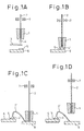
- Figs. 1A-1D show ultrasonic-assisted heat-pressing bonding, for interconnection and loop formation, in which 1 is a capillary, 2 is a gold wire, 3 is a torch electrode, 4 is a metal ball, 5 is an Al electrode, 6 is a semiconductor element, 7 is a clamper and 8 is a lead.
- the ball neck portion is forcefully bent in the direction opposite to the loop formation direction during the loop forming process in order to stabilize the aforementioned loop shape to deform it, and then the final loop is actually formed, thus forming a loop by "reverse deformation".
- Many semiconductor devices are used under exposure to high temperature due to heating by operating circuits or external environments. It has therefore been sought to minimize wire breakage even after exposure to harsh heat-cycle environments after formation of loops by reverse deformation in this manner.
- high pressure bonding can produce aberrations such as collapse of high loop shapes, and it is therefore desirable to use low pressure bonding.
- a low pressure bonding poses the problem of low junction strength.
- a desired goal for high loop wiring has therefore been to improve the junction strength even with a low pressure bonding at the second side junction, while maintaining the high loop shape.
- the present inventors have attempted to produce gold wires satisfying these properties, but the tensile strength has been insufficient.
- the present invention provides a gold wire for semiconductor element bonding which comprises 11-20 ppm by mass of Ag, 1-9 ppm by mass of Pt, 1-15 ppm by mass of Y, 1-15 ppm by mass of La, and 1-15 ppm by mass of Eu, with either or both 1-20 ppm by mass of Ca and 1-10 ppm by mass of Be, the total amount of the above elements being under 100 ppm by mass, the remainder being Au and unavoidable impurities.
- a method of wire bonding of a semiconductor element with leads using the above gold wire is also provided.
- Figs. 1A to 1D are a set of illustrations showing a method for ultrasonic-assisted heat-pressing bonding between an electrode of a semiconductor element and an external lead using gold wire.
- the starting gold used is preferably high purity gold which has been purified to at least 99.99 wt%.
- the purity is more preferably at least 99.995 wt%, and most preferably at least 99.999 wt%. Higher purity gold is preferred because it can minimize the effects of harmful components.
- the aforementioned objects can be achieved with an Ag content of 11-20 ppm by mass when the gold alloy wire used for the invention contains the prescribed amounts of Pt, Y, La, Eu and Ca or Be.
- the aforementioned objects can be achieved with a Pt content of 1-9 ppm by mass when the alloy gold wire used for the invention contains the prescribed amounts of Ag, Y, La, Eu and, Ca or Be.
- the aforementioned objects can be achieved with a Y content of 1-15 ppm by mass when the alloy gold wire used for the invention contains the prescribed amounts of Ag, Pt, La, Eu and Ca or Be.
- the Y content is therefore limited to 1-15 ppm by mass when in the presence of the prescribed amounts of Ag, etc.
- the aforementioned objects can be achieved with an La content of 1-15 ppm by mass when the alloy gold wire used for the invention contains the prescribed amounts of Ag, Pt, Y, Eu and Ca or Be.
- the La content is therefore limited to 1-15 ppm by mass when in the presence of the prescribed amounts of Ag, etc.
- the aforementioned object can be achieved with a Eu content of 1-15 ppm by mass when the alloy gold wire used for the invention contains the prescribed amounts of Ag, Pt, Y, La and Ca or Be.
- the Eu content is therefore limited to 1-15 ppm by mass when in the presence of the prescribed amounts of Ag, etc.
- the aforementioned object can be achieved with either or both a Ca content of 1-20 ppm by mass and a Be content of 1-10 ppm by mass when the alloy gold wire used for the invention contains the prescribed amounts of Ag, Pt, Y, La and Eu.
- Either or both the Ca content and the Be content are therefore limited to 1-20 ppm by mass and 1-10 ppm by mass, respectively, when in the presence of the prescribed amounts of Ag, etc.
- the gold wire of the invention is used for bonding between electrodes of a semiconductor element and external leads, and the bonding method is usually bonding and interconnecting according to the ball bonding method, such as shown in Fig. 1A-1D. This is preferably employed with a so-called "high loop" in which wire 2' is high as in Fig. 1D. A method of bonding by the ball bonding method will now be explained with reference to Figs. 1A to 1D.
- the gold wire 2 is inserted through a capillary 1, and an electric torch 3 is situated opposite the tip end of the wire 2 and creates an electric-discharge reaching to the gold wire 2, thus heating the tip of the gold wire 2 and fusing it to form a ball 4.
- the capillary 1 is lowered for pressing bonding onto an Al electrode 5 on the semiconductor element 6.
- ultrasonic vibrations (not shown) are passed through the capillary 1 and applied thereto while the semiconductor element 6 is heated with a heater block, so that the ball 4 is heat-pressing bonded, becoming a pressure bonded ball 4'.
- the capillary 1 is moved and lowered onto an external lead 8 following a prescribed trajectory.
- Ultrasonic vibrations (not shown) are passed through the capillary 1 and applied thereto while the external lead 8 is heated with a heater block, so that the surface of the gold wire 2 is heat-pressing bonded to the external lead 8.
- the clamper 7 is raised while clamping the gold wire 2, thus cutting the gold wire 2 and completing the wiring.
- the wiring section is then sealed with a resin to complete the semiconductor device.
- a test material was used as a bonding wire for ultrasonic heat-pressing bonding onto electrodes of an IC chip using a high-speed automatic bonder. After ball bonding with an ultrasonic output of 0.196 W and a load of 0.49 N, the capillary was first moved in the direction opposite to the loop formation direction, the reverse angle was set to an angle of 60° with respect to the vertical, the ball neck section was forcefully bent for deformation to form and maintain an inner warp, and this was then joined to an external lead to form a regular loop (wiring). A total of 200 pin wirings were formed for each IC chip.
- the wiring sample was sealed with a resin and then subjected 2000 times to a maximum harshness heat cycle test with a cycle of -55°C x 30 minutes and 160°C x 30 minutes.
- a maximum harshness heat cycle test with a cycle of -55°C x 30 minutes and 160°C x 30 minutes.
- One hundred IC chips were prepared for testing, and the presence of wire breakage was determined by a conduction test. The number of ICs with wire breakage sections are shown in Table 1 as the breakage rate (%).
- the aforementioned heat cycle test was carried out in the same manner except that the wiring was formed without reverse deformation, and bondings were formed to a total of 8 IC chips. Two hundreds wires from arbitrarily selected ICs were then measured for loop height using a length measuring microscope. The average value is listed in Table 1 as the loop height.
- Low output contact bonding was carried out with an ultrasonic output of 0.157 W (commonly 0.235 W) and a load of 0.392 N (commonly 0.588 N) as the pressing bonding conditions for the second side (lead side) as shown in Fig. 1C.
- the center section of the wiring was cut, the tip of the lead side wire was grasped with tweezers supplied with the bond tester and the load required for the wire lifted up from the anchored lead to peel from the lead was measured. A total of 50 points were measured, and the average value is listed in Table 1 as the second side peel strength with low pressure bonding.
- Gold alloy wires were produced and tested in the same manner as Example 1, except that the amounts of the elements were changed as shown in Tables 1 and 2. The test results are also shown in Tables 1 and 2.
- the construction of the present invention therefore achieves the object of the invention which is to provide a gold wire for semiconductor element bonding wherein the total amount of the added elements is no greater than 100 ppm by mass and which allows, firstly, reverse deformation in order to minimize wire breakage even upon exposure to harsh heat cycle environments after formation of loops, which allows, secondly, formation of high loops at above a prescribed height, which allows, thirdly, maintenance of junction strength above a prescribed value even with a low pressure bonding at the second side junction in order to maintain the high loop shape, and which allows, fourthly, maintenance of a high tensile strength.
- the Ag amount was increased above 20 ppm by mass or the Pt amount was increased above 9 ppm by mass in the composition of 15 ppm by mass of Ag, 5 ppm by mass of Pt, 10 ppm by mass of Y, 10 ppm by mass of La, 10 ppm by mass of Eu, 10 ppm by mass of Ca and 5 ppm by mass of Be; both of these samples allowed a high loop height, but the second side peel strength with low pressure bonding was 8-12 mN and the tensile strength was 127-129 mN, and therefore the samples of the invention were highly superior for achieving the object of the invention.
- Comparative Example 13 which contained 15 ppm by mass of Ag, 5 ppm by mass of Pt, 10 ppm by mass of Y, 10 ppm by mass of La, 30 ppm by mass of Ca and 5 ppm by mass of Be in a composition containing no Eu, had a loop height of 131 ⁇ m and a second side peel strength with low pressure bonding of 20 mN, and therefore the samples of the invention were highly superior for achieving the object of the invention.
Landscapes
- Wire Bonding (AREA)
- Die Bonding (AREA)
Applications Claiming Priority (2)
| Application Number | Priority Date | Filing Date | Title |
|---|---|---|---|
| JP2000183521 | 2000-06-19 | ||
| JP2000183521A JP3323185B2 (ja) | 2000-06-19 | 2000-06-19 | 半導体素子接続用金線 |
Publications (3)
| Publication Number | Publication Date |
|---|---|
| EP1168439A2 true EP1168439A2 (de) | 2002-01-02 |
| EP1168439A3 EP1168439A3 (de) | 2002-04-10 |
| EP1168439B1 EP1168439B1 (de) | 2007-04-11 |
Family
ID=18684099
Family Applications (1)
| Application Number | Title | Priority Date | Filing Date |
|---|---|---|---|
| EP01250061A Expired - Lifetime EP1168439B1 (de) | 2000-06-19 | 2001-02-27 | Goldverbindungsdraht für ein Halbleiterbauelement |
Country Status (8)
| Country | Link |
|---|---|
| EP (1) | EP1168439B1 (de) |
| JP (1) | JP3323185B2 (de) |
| KR (1) | KR100695925B1 (de) |
| CN (1) | CN1267991C (de) |
| DE (1) | DE60127768T2 (de) |
| MY (1) | MY136914A (de) |
| SG (1) | SG87207A1 (de) |
| TW (1) | TW480635B (de) |
Cited By (1)
| Publication number | Priority date | Publication date | Assignee | Title |
|---|---|---|---|---|
| WO2006057230A1 (ja) | 2004-11-26 | 2006-06-01 | Tanaka Denshi Kogyo K.K. | 半導体素子用Auボンディングワイヤ |
Families Citing this family (5)
| Publication number | Priority date | Publication date | Assignee | Title |
|---|---|---|---|---|
| KR100899322B1 (ko) * | 2004-09-30 | 2009-05-27 | 타나카 덴시 코오교오 카부시키가이샤 | Au 합금 본딩·와이어 |
| JP4595018B2 (ja) * | 2009-02-23 | 2010-12-08 | 株式会社新川 | 半導体装置の製造方法およびボンディング装置 |
| CN107644716B (zh) * | 2017-09-15 | 2019-09-13 | 绍兴市高砚智生物科技有限公司 | 添加蜜胺甲醛树脂的复合铜丝生产方法 |
| CN107958850A (zh) * | 2017-11-28 | 2018-04-24 | 宁波尚进自动化科技有限公司 | 一种焊点焊接质量监控系统及其监控方法 |
| CN109811176A (zh) * | 2019-03-25 | 2019-05-28 | 杭州辰卓科技有限公司 | 一种电子器件封装高阻尼键合线用金合金及其工艺 |
Family Cites Families (11)
| Publication number | Priority date | Publication date | Assignee | Title |
|---|---|---|---|---|
| JPS5649534A (en) * | 1979-09-28 | 1981-05-06 | Tanaka Kikinzoku Kogyo Kk | Bonding wire for semiconductor device |
| GB2116208B (en) * | 1981-12-04 | 1985-12-04 | Mitsubishi Metal Corp | Fine gold alloy wire for bonding of a semiconductor device |
| JPS61110735A (ja) * | 1984-10-31 | 1986-05-29 | Tatsuta Electric Wire & Cable Co Ltd | 耐熱性に優れた金合金 |
| JPS62228440A (ja) * | 1986-03-28 | 1987-10-07 | Matsuda Kikinzoku Kogyo Kk | 半導体素子ボンデイング用金線 |
| JP3337049B2 (ja) * | 1995-05-17 | 2002-10-21 | 田中電子工業株式会社 | ボンディング用金線 |
| US5945065A (en) * | 1996-07-31 | 1999-08-31 | Tanaka Denshi Kogyo | Method for wedge bonding using a gold alloy wire |
| JP3657087B2 (ja) * | 1996-07-31 | 2005-06-08 | 田中電子工業株式会社 | ウエッジボンディング用金合金線 |
| US5745418A (en) * | 1996-11-25 | 1998-04-28 | Macronix International Co., Ltd. | Flash memory mass storage system |
| JP3573321B2 (ja) * | 1996-12-11 | 2004-10-06 | 住友金属鉱山株式会社 | Auボンディングワイヤー |
| JP3669809B2 (ja) * | 1997-04-25 | 2005-07-13 | 田中電子工業株式会社 | 半導体素子ボンディング用金合金線 |
| JP2000040710A (ja) * | 1998-07-24 | 2000-02-08 | Sumitomo Metal Mining Co Ltd | ボンディング用金合金細線 |
-
2000
- 2000-06-19 JP JP2000183521A patent/JP3323185B2/ja not_active Expired - Lifetime
-
2001
- 2001-02-23 TW TW090104260A patent/TW480635B/zh not_active IP Right Cessation
- 2001-02-24 SG SG200101081A patent/SG87207A1/en unknown
- 2001-02-26 KR KR1020010009692A patent/KR100695925B1/ko not_active Expired - Fee Related
- 2001-02-27 DE DE60127768T patent/DE60127768T2/de not_active Expired - Lifetime
- 2001-02-27 EP EP01250061A patent/EP1168439B1/de not_active Expired - Lifetime
- 2001-02-28 CN CNB011089202A patent/CN1267991C/zh not_active Expired - Fee Related
- 2001-02-28 MY MYPI20010898A patent/MY136914A/en unknown
Cited By (3)
| Publication number | Priority date | Publication date | Assignee | Title |
|---|---|---|---|---|
| WO2006057230A1 (ja) | 2004-11-26 | 2006-06-01 | Tanaka Denshi Kogyo K.K. | 半導体素子用Auボンディングワイヤ |
| EP1830398A4 (de) * | 2004-11-26 | 2012-06-06 | Tanaka Electronics Ind | Au-bondierungsdraht für ein halbleiterelement |
| US8440137B2 (en) * | 2004-11-26 | 2013-05-14 | Tanaka Denshi Kogyo K.K. | Au bonding wire for semiconductor device |
Also Published As
| Publication number | Publication date |
|---|---|
| CN1267991C (zh) | 2006-08-02 |
| DE60127768D1 (de) | 2007-05-24 |
| CN1330404A (zh) | 2002-01-09 |
| TW480635B (en) | 2002-03-21 |
| JP2002009101A (ja) | 2002-01-11 |
| KR100695925B1 (ko) | 2007-03-20 |
| KR20010113459A (ko) | 2001-12-28 |
| EP1168439A3 (de) | 2002-04-10 |
| JP3323185B2 (ja) | 2002-09-09 |
| DE60127768T2 (de) | 2007-12-27 |
| EP1168439B1 (de) | 2007-04-11 |
| SG87207A1 (en) | 2002-03-19 |
| MY136914A (en) | 2008-11-28 |
Similar Documents
| Publication | Publication Date | Title |
|---|---|---|
| KR20030033066A (ko) | 반도체용 본딩 와이어 및 그 제조 방법 | |
| EP1160344B1 (de) | Golddraht für Halbleiterverbindungsbauelement und Verfahren zur Herstellung eines Halbleiterverbindungsbauelementes | |
| US6159420A (en) | Gold alloy wire and method for making a bump | |
| EP1168439A2 (de) | Goldverbindungsdraht für ein Halbleiterbauelement | |
| JPS62228440A (ja) | 半導体素子ボンデイング用金線 | |
| JP3697227B2 (ja) | 半導体装置用金ボンディングワイヤ及びその製造方法 | |
| KR101158547B1 (ko) | 볼 본딩용 금합금선 | |
| JP3579493B2 (ja) | 半導体素子用金合金細線 | |
| JP3657087B2 (ja) | ウエッジボンディング用金合金線 | |
| JP4134261B1 (ja) | ボールボンディング用金合金線 | |
| JPH0425336B2 (de) | ||
| KR0145549B1 (ko) | 반도체소자용 금합금 세선 | |
| JPH1098062A (ja) | ウエッジボンディング用金合金線 | |
| JP3426473B2 (ja) | 半導体素子用金合金細線 | |
| JPH02250934A (ja) | 半導体素子ボンディング用Au合金極細線 | |
| JPWO1994024322A1 (ja) | 半導体素子用金合金細線 | |
| JP3586909B2 (ja) | ボンディングワイヤ | |
| JP4117973B2 (ja) | ボンディング用金合金線 | |
| JPH09198917A (ja) | 半導体素子用金合金細線 | |
| JPH02251156A (ja) | 半導体素子ボンディング用金合金線 |
Legal Events
| Date | Code | Title | Description |
|---|---|---|---|
| PUAI | Public reference made under article 153(3) epc to a published international application that has entered the european phase |
Free format text: ORIGINAL CODE: 0009012 |
|
| AK | Designated contracting states |
Kind code of ref document: A2 Designated state(s): DE FR GB NL Kind code of ref document: A2 Designated state(s): AT BE CH CY DE DK ES FI FR GB GR IE IT LI LU MC NL PT SE TR |
|
| AX | Request for extension of the european patent |
Free format text: AL;LT;LV;MK;RO;SI |
|
| PUAL | Search report despatched |
Free format text: ORIGINAL CODE: 0009013 |
|
| AK | Designated contracting states |
Kind code of ref document: A3 Designated state(s): AT BE CH CY DE DK ES FI FR GB GR IE IT LI LU MC NL PT SE TR |
|
| AX | Request for extension of the european patent |
Free format text: AL;LT;LV;MK;RO;SI |
|
| 17P | Request for examination filed |
Effective date: 20020405 |
|
| AKX | Designation fees paid |
Free format text: DE FR GB NL |
|
| 17Q | First examination report despatched |
Effective date: 20050203 |
|
| GRAP | Despatch of communication of intention to grant a patent |
Free format text: ORIGINAL CODE: EPIDOSNIGR1 |
|
| GRAS | Grant fee paid |
Free format text: ORIGINAL CODE: EPIDOSNIGR3 |
|
| GRAA | (expected) grant |
Free format text: ORIGINAL CODE: 0009210 |
|
| AK | Designated contracting states |
Kind code of ref document: B1 Designated state(s): DE FR GB NL |
|
| REG | Reference to a national code |
Ref country code: GB Ref legal event code: FG4D |
|
| REF | Corresponds to: |
Ref document number: 60127768 Country of ref document: DE Date of ref document: 20070524 Kind code of ref document: P |
|
| ET | Fr: translation filed | ||
| PLBE | No opposition filed within time limit |
Free format text: ORIGINAL CODE: 0009261 |
|
| STAA | Information on the status of an ep patent application or granted ep patent |
Free format text: STATUS: NO OPPOSITION FILED WITHIN TIME LIMIT |
|
| 26N | No opposition filed |
Effective date: 20080114 |
|
| PGFP | Annual fee paid to national office [announced via postgrant information from national office to epo] |
Ref country code: DE Payment date: 20130220 Year of fee payment: 13 Ref country code: GB Payment date: 20130228 Year of fee payment: 13 Ref country code: FR Payment date: 20130301 Year of fee payment: 13 |
|
| PGFP | Annual fee paid to national office [announced via postgrant information from national office to epo] |
Ref country code: NL Payment date: 20130216 Year of fee payment: 13 |
|
| REG | Reference to a national code |
Ref country code: DE Ref legal event code: R119 Ref document number: 60127768 Country of ref document: DE |
|
| REG | Reference to a national code |
Ref country code: NL Ref legal event code: V1 Effective date: 20140901 |
|
| GBPC | Gb: european patent ceased through non-payment of renewal fee |
Effective date: 20140227 |
|
| PG25 | Lapsed in a contracting state [announced via postgrant information from national office to epo] |
Ref country code: NL Free format text: LAPSE BECAUSE OF NON-PAYMENT OF DUE FEES Effective date: 20140901 |
|
| REG | Reference to a national code |
Ref country code: FR Ref legal event code: ST Effective date: 20141031 |
|
| REG | Reference to a national code |
Ref country code: DE Ref legal event code: R119 Ref document number: 60127768 Country of ref document: DE Effective date: 20140902 |
|
| PG25 | Lapsed in a contracting state [announced via postgrant information from national office to epo] |
Ref country code: DE Free format text: LAPSE BECAUSE OF NON-PAYMENT OF DUE FEES Effective date: 20140902 Ref country code: FR Free format text: LAPSE BECAUSE OF NON-PAYMENT OF DUE FEES Effective date: 20140228 Ref country code: GB Free format text: LAPSE BECAUSE OF NON-PAYMENT OF DUE FEES Effective date: 20140227 |