EP1164535A1 - Dispositif de production d'un champ électromagnétique pour transpondeur - Google Patents
Dispositif de production d'un champ électromagnétique pour transpondeur Download PDFInfo
- Publication number
- EP1164535A1 EP1164535A1 EP01410056A EP01410056A EP1164535A1 EP 1164535 A1 EP1164535 A1 EP 1164535A1 EP 01410056 A EP01410056 A EP 01410056A EP 01410056 A EP01410056 A EP 01410056A EP 1164535 A1 EP1164535 A1 EP 1164535A1
- Authority
- EP
- European Patent Office
- Prior art keywords
- oscillating circuit
- concentrator
- transponder
- terminal
- electromagnetic field
- Prior art date
- Legal status (The legal status is an assumption and is not a legal conclusion. Google has not performed a legal analysis and makes no representation as to the accuracy of the status listed.)
- Granted
Links
Images

Classifications
-
- G—PHYSICS
- G06—COMPUTING OR CALCULATING; COUNTING
- G06K—GRAPHICAL DATA READING; PRESENTATION OF DATA; RECORD CARRIERS; HANDLING RECORD CARRIERS
- G06K7/00—Methods or arrangements for sensing record carriers, e.g. for reading patterns
- G06K7/0008—General problems related to the reading of electronic memory record carriers, independent of its reading method, e.g. power transfer
-
- G—PHYSICS
- G06—COMPUTING OR CALCULATING; COUNTING
- G06K—GRAPHICAL DATA READING; PRESENTATION OF DATA; RECORD CARRIERS; HANDLING RECORD CARRIERS
- G06K19/00—Record carriers for use with machines and with at least a part designed to carry digital markings
- G06K19/06—Record carriers for use with machines and with at least a part designed to carry digital markings characterised by the kind of the digital marking, e.g. shape, nature, code
- G06K19/067—Record carriers with conductive marks, printed circuits or semiconductor circuit elements, e.g. credit or identity cards also with resonating or responding marks without active components
- G06K19/07—Record carriers with conductive marks, printed circuits or semiconductor circuit elements, e.g. credit or identity cards also with resonating or responding marks without active components with integrated circuit chips
- G06K19/077—Constructional details, e.g. mounting of circuits in the carrier
- G06K19/07749—Constructional details, e.g. mounting of circuits in the carrier the record carrier being capable of non-contact communication, e.g. constructional details of the antenna of a non-contact smart card
- G06K19/07766—Constructional details, e.g. mounting of circuits in the carrier the record carrier being capable of non-contact communication, e.g. constructional details of the antenna of a non-contact smart card comprising at least a second communication arrangement in addition to a first non-contact communication arrangement
- G06K19/07767—Constructional details, e.g. mounting of circuits in the carrier the record carrier being capable of non-contact communication, e.g. constructional details of the antenna of a non-contact smart card comprising at least a second communication arrangement in addition to a first non-contact communication arrangement the first and second communication means being two different antennas types, e.g. dipole and coil type, or two antennas of the same kind but operating at different frequencies
-
- G—PHYSICS
- G06—COMPUTING OR CALCULATING; COUNTING
- G06K—GRAPHICAL DATA READING; PRESENTATION OF DATA; RECORD CARRIERS; HANDLING RECORD CARRIERS
- G06K7/00—Methods or arrangements for sensing record carriers, e.g. for reading patterns
- G06K7/10—Methods or arrangements for sensing record carriers, e.g. for reading patterns by electromagnetic radiation, e.g. optical sensing; by corpuscular radiation
- G06K7/10009—Methods or arrangements for sensing record carriers, e.g. for reading patterns by electromagnetic radiation, e.g. optical sensing; by corpuscular radiation sensing by radiation using wavelengths larger than 0.1 mm, e.g. radio-waves or microwaves
- G06K7/10158—Methods or arrangements for sensing record carriers, e.g. for reading patterns by electromagnetic radiation, e.g. optical sensing; by corpuscular radiation sensing by radiation using wavelengths larger than 0.1 mm, e.g. radio-waves or microwaves methods and means used by the interrogation device for reliably powering the wireless record carriers using an electromagnetic interrogation field
- G06K7/10178—Methods or arrangements for sensing record carriers, e.g. for reading patterns by electromagnetic radiation, e.g. optical sensing; by corpuscular radiation sensing by radiation using wavelengths larger than 0.1 mm, e.g. radio-waves or microwaves methods and means used by the interrogation device for reliably powering the wireless record carriers using an electromagnetic interrogation field including auxiliary means for focusing, repeating or boosting the electromagnetic interrogation field
-
- G—PHYSICS
- G06—COMPUTING OR CALCULATING; COUNTING
- G06K—GRAPHICAL DATA READING; PRESENTATION OF DATA; RECORD CARRIERS; HANDLING RECORD CARRIERS
- G06K7/00—Methods or arrangements for sensing record carriers, e.g. for reading patterns
- G06K7/10—Methods or arrangements for sensing record carriers, e.g. for reading patterns by electromagnetic radiation, e.g. optical sensing; by corpuscular radiation
- G06K7/10009—Methods or arrangements for sensing record carriers, e.g. for reading patterns by electromagnetic radiation, e.g. optical sensing; by corpuscular radiation sensing by radiation using wavelengths larger than 0.1 mm, e.g. radio-waves or microwaves
- G06K7/10316—Methods or arrangements for sensing record carriers, e.g. for reading patterns by electromagnetic radiation, e.g. optical sensing; by corpuscular radiation sensing by radiation using wavelengths larger than 0.1 mm, e.g. radio-waves or microwaves using at least one antenna particularly designed for interrogating the wireless record carriers
- G06K7/10336—Methods or arrangements for sensing record carriers, e.g. for reading patterns by electromagnetic radiation, e.g. optical sensing; by corpuscular radiation sensing by radiation using wavelengths larger than 0.1 mm, e.g. radio-waves or microwaves using at least one antenna particularly designed for interrogating the wireless record carriers the antenna being of the near field type, inductive coil
Definitions
- the present invention relates to systems using electromagnetic transponders, i.e. transmitters and / or receivers (generally mobile) likely to be interrogated, contactless and wireless, by a unit (usually fixed) called reading and / or writing terminal.
- transponders extract the power required for circuits electronic they have a high frequency field radiated by an antenna from the read and write terminal.
- the invention applies to such systems, whether they are systems read-only, i.e. including a terminal just reading the data from one or more transponders, or read-write systems in which the transponders contain data which can be modified by the terminal.
- Systems using electromagnetic transponders are based on the use of oscillating circuits including a winding forming an antenna on the transponder side and on the terminal side of readind, writing. These circuits are intended to be coupled by near magnetic field when the transponder enters the read-write terminal field.
- FIG. 1 very schematically represents and simplified, a classic example of a data exchange system between a read-write terminal 1 and a transponder 10 of the type to which the present invention applies.
- terminal 1 is essentially made up of a series oscillating circuit, formed of an inductance L1, in series with a capacitor C1 and a resistor R1, between a terminal 2 output of an antenna amplifier or coupler (not shown) and a reference terminal 3 (generally, ground).
- the antenna coupler is part of a circuit 4 for controlling the circuit oscillating and exploiting the data received including, among others, a modulator / demodulator and a microprocessor processing of orders and data. The exploitation of data received is based on a measurement of the current in the circuit oscillating or voltage across its terminals.
- Terminal circuit 4 generally communicates with different input / output circuits (keyboard, screen, means of exchange with a server, etc.) and / or treatments not shown. Read-write terminal circuits generally draw the energy necessary for their operation a supply circuit (not shown) connected, for example, to the electrical distribution network or to batteries.
- a transponder 10 intended to cooperate with a terminal 1, essentially comprises a parallel oscillating circuit formed inductance L2 in parallel with a capacitor C2 between two terminals 11 and 12 for input of circuits 13 for controlling and treatment.
- Terminals 11 and 12 are, in practice, connected to the entry of a rectifying means (not shown) including outputs constitute DC power supply terminals internal to the transponder.
- These circuits generally include, essentially a microprocessor capable of communicating with other elements (for example, a memory), a demodulator of the signals received from terminal 1 and a modulator to transmit information to the terminal.
- Oscillating circuits of the terminal and the transponder are generally tuned on the same frequency corresponding to the frequency of an excitation signal of the oscillating circuit of the thick headed.
- This high frequency signal (for example 13.56 MHz) is used only transmission carrier but also carrier remote power supply to the transponder (s) found in the terminal field.
- a 10 transponder finds in the field of a terminal 1 a high frequency voltage is generated at terminals 11 and 12 of its resonant circuit.
- This tension after rectification and possible capping, is intended to supply the supply voltage of the electronic circuits 13 of the transponder. For reasons of clarity, the means of straightening, capping, and supplying power not shown in Figure 1.
- the transmission of data from the transponder to a terminal is generally done by modulating the charge constituted by the resonant circuit L2, C2.
- the load variation takes place at the rate of a subcarrier, so-called retromodulation, frequency (for example 847.5 kHz) lower than that of the carrier.
- a terminal 1 has a planar antenna L1 formed of some circular turns (usually one or two turns) of relatively large diameter (for example of a value data between a few cm and 1 m) and the L2 antenna of a transponder (for example, a credit card size card) consists of a few turns (most often between two and five turns) rectangular in a relatively diameter small (turns 5 to 8 cm per side) compared to the diameter of the L1 antenna.
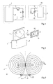
- FIG 2 is a schematic perspective view a terminal and a transponder illustrating a classic example antennas.
- the electronic circuits 4 of terminal 1, likewise that capacitor C1 and resistor R1 are generally contained in a base 6.
- the antenna L1 is, for example, carried by a printed circuit board 7 projecting from the base 6.
- Transponder side 10 it is assumed that it is a smart card integrating circuits 13 and including the L2 antenna includes two rectangular and coplanar turns describing approximately the periphery of the card 10.
- the capacitor C2 shown separate from circuits 13 is generally carried out by being integrated into the chip.
- transponder systems are generally limited in range, i.e. at a certain distance (d, figure 2) of the terminal, the magnetic field is insufficient to correctly supply a transponder.
- the minimum field is generally between 0.1 and 1 A / m depending on consumption of the transponder which essentially differs according to whether it is or not equipped with a microprocessor.
- the range of remote power supply depends on the amount of magnetic flux emitted by the terminal or reader, which can be "picked up" by a transponder. This quantity depends directly the coupling factor between the antennas L1 and L2, which represents the proportion of flux recovered by the transponder.
- the coupling factor (between 0 and 1) depends on several factors among which, essentially, the mutual inductance between the antennas L1 and L2 and the respective size of the antennas, and the tuning of the oscillating circuits on the carrier frequency high frequency excitation. For sizes and one mutual inductance data, the coupling is maximum when the oscillating circuits of the terminal and the transponder are both tuned to the frequency of the remote power carrier.
- Figure 3 shows schematically a classic example distribution of the magnetic field lines produced by a terminal 1 in the field of which there is a transponder 10.
- the representation of Figure 3 corresponds, for example, to a section of the representation of figure 2 including the two L1 and L2 antennas.
- an arbitrary meaning has been indicated current flow I in the inductors L1 and L2.
- As the current is alternating, for example, its meaning in a given moment.
- Magnetic field lines 15 wind around the component conductor of the antenna L1 and are, in the sectional view of FIG. 3, symmetrical with respect to an axis 16 of symmetry of the antenna L1.
- the transponder 10 captures energy when its L2 antenna is located in the terminal field.
- a classic solution to increase the range is to increase the size of the terminal's antenna L1. To preserve the magnetic field, we must then increase the intensity of the current of the excitation signal in the same ratio.
- a first disadvantage of such a solution is that it increases the power necessary excitation of the system.
- a second drawback of such a solution is that such an increase in current remains limited by the constitution of the generator and requires a large dimensioning of the components (in particular, a large section of the conductor constituting the antenna L1). Of more, the losses are proportional to the square of the current.
- the document EP-A-0333388 describes a transfer circuit of energy to two windings sharing the same core magnetic, which are mechanically and electrically linked, and which are not placed at a distance from each other.
- the present invention aims to overcome the drawbacks conventional transponder systems.
- the invention aims, in particular, to improve the range and / or the signal level available at a given distance, from a transponder read and / or write terminal.
- the invention also aims to propose a solution which is compatible with existing systems. More precisely, the invention aims to propose a solution requiring no modification of transponders and preferably no modification of the read-write terminal.
- the invention further aims to propose a solution that is little energy-hungry, requiring no specific power supply.
- the present invention provides an antenna producing an electromagnetic field at by means of a first oscillating circuit excited by a high signal frequency, comprising, at a distance from the first oscillating circuit, a second oscillating circuit, passive, unloaded and devoid of magnetic core, forming a flux concentrator magnetic intended to be picked up by a transponder by means of a third oscillating circuit.
- the second oscillating circuit and the first oscillating circuit have approximately identical natural resonant frequencies preferably chosen to correspond approximately to the frequency of the excitation signal of the first oscillating circuit.
- the second oscillating circuit includes at least one inductance plane whose overall surface fits into an upper surface to that in which an inductance is registered that includes the third oscillating circuit of a transponder intended to receive the magnetic flux.
- the second oscillating circuit includes at least one inductance plane whose overall surface fits into an upper surface or equal to that in which an inductance is registered that comprises the first oscillating circuit.
- the orientation of the plans in which inductances are inscribed planes of the first and second oscillating circuits is chosen according to the preferred operating zones desired.
- the concentrator has at least two voltage or current.
- the present invention also provides a concentrator of magnetic flux suitable for cooperating with an element of generation of electromagnetic field, this concentrator being consisting of an oscillating circuit provided with a single inductance in parallel with a capacitor.
- the concentrator consists of n oscillating circuits with inductances coplanar.
- the concentrator has n coplanar inductances, in parallel with a single capacitor.
- the present invention also provides a system exchange of information between an electromagnetic transponder and a read and / or write terminal.
- a feature of the present invention is provide, in association with a first oscillating circuit of generation of an electromagnetic field, at least a second passive and unloaded oscillating circuit to deform the lines field of the first circuit.
- This second oscillating circuit is a parallel circuit (plug) which does not supply any load or receives electrical excitation signal.
- this resonant circuit specific to the invention is tuned on the frequency of the excitation carrier of the first circuit oscillating.
- a flux concentrator associated with the terminal.
- This flux concentrator comprises at least one planar antenna having, preferably a size as it fits into a surface greater than or equal to that in which enrolled the L1 antenna of the terminal.
- these antennas are without magnetic core to conduct the magnetic flux so that they can be placed at a distance from each other.
- Figure 4 very schematically shows a first embodiment of the present invention.
- the representation of Figure 4 is close to that of Figure 2 previously described.
- terminal 1 and the transponder 10 have conventional structures such as described in relation to Figure 2.
- the device for producing an electromagnetic field comprises not only the terminal 1 provided with the oscillating circuit L1-C1 for generating the field, but also at least one element 20 concentrating the magnetic flux.
- This element 20 constitutes a passive resonant circuit that is not electrically charged and not activated, here formed of an inductance L3, the two terminals of which are connected to the respective electrodes of a capacitor C3.
- the inductor L3 can be formed, like the inductor L1, on a printed circuit board 21.
- the oscillating circuit of the flux concentrator 20 is preferably tuned to the same frequency as the oscillating circuit of the terminal 1.
- the orientation of the plan in which the antenna is located of the concentrator with respect to the plane of the terminal antenna can be used to favor an operation in an axis different from normal to the terminal antenna plan, or in a localized area where the field lines are concentrated.
- Figure 5 illustrates this phenomenon by representing a schematic sectional view of the device of Figure 4 illustrating the appearance of the field lines.
- the representation of figure 5 is similar to that of Figure 3 described above.
- a transponder 10 can be placed anywhere between terminal 1 and concentrator 20 in able to capture sufficient energy for its food.
- a transponder can be remotely powered by being placed on the other side but then near the concentrator with respect to the terminal.
- the distance D between the concentrator 20 of terminal 1 is chosen according to the sizes and geometries L1 and L3 antennas. Indeed, there is a distance D maximum between the terminal and the concentrator beyond which the latter will have no effect. This maximum distance corresponds to the distance limit for which, when a transponder is placed between the terminal and the concentrator, this transponder remains remotely powered continuously regardless of its position between the terminal and the concentrator.
- An advantage of the present invention is that the increase range of the system is obtained almost without consumption additional. Indeed, the only consumption of the concentrator of flux corresponds to the dissipation of its components L3 and C3 which are only weakly resistive. For a given current I excitation of the terminal's oscillating circuit, the range of a system, equipped with a concentrator whose size of the antenna corresponds to that of the L1 antenna, is approximately doubled compared to that of a conventional terminal excited by the same current.
- Another advantage of the present invention is that its implementation requires no modification of the terminal or transponder.
- the absence of a magnetic core for channeling the flow makes the terminal and the flow concentrator mechanically independent of each other. Just place a correctly sized flow concentrator next to a terminal at an adequate distance to increase the scope of the system.
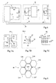
- Figure 6 shows, in a simplified way, the diagram electric equivalent of a field production device electromagnetic to a transponder according to a second embodiment of the present invention.
- the representation of Figure 6 is to be compared to that of Figure 1 previously described.
- a feature of this second embodiment is that the oscillating circuit of the flux concentrator 20 'is also used as an element for detecting any information emitted by the transponder 10.
- the transmission of information from the transponder to the reader is made by modulating, at the rate of a subcarrier, the load formed by the transponder on the oscillating circuit of the terminal.
- this load variation can also be detected well on the terminal side than on the concentrator side.
- the two terminals 22 and 23 can then be connected (connections 24 and 25) to the circuit 4 for processing data from terminal 1 '(for example, at the input terminals of a demodulator).
- care will be taken to what this measure can be considered not to affect the unloaded nature of the resonant circuit of the concentrator.
- the antenna of the oscillating circuit of flux concentrator preferably fits into a surface greater than or equal to the surface in which is inscribed the terminal antenna and preferably substantially the same area.
- the space requirement approximately identical of the L1 and L3 antennas is respected by providing an L3 antenna having substantially the same shape and size of antenna L1 of terminal 1 or 1 '.
- Figures 7A, 7B and 7C illustrate a third mode of the present invention in which the condition above size is respected by providing, side concentrator 30, a network of several inductors associated in at most each parallel to a capacitor.
- a single capacitor for all the inductances of the network (four inductors having substantially the same size and the same value in the example of Figures 7A to 7C).
- Figure 7A is a view of a first face 30-1 of a circuit board printed on which, for example, the inductors are made L31 to L34.
- FIG. 7B is a view of the second face 30-2 of the printed circuit board.
- Figure 7C shows the equivalent electrical diagram of concentrator 30 according to this third embodiment.
- the inductors L31 to L34 are associated in parallel with capacitor C3 '.
- the four inductors are connected by a first end on the first side 30-1 while their other ends are connected to via 36, 37, 38 and 39 connecting to the second face.
- Second side 30-2 side the via of the second ends are connected together to a first electrode of the capacitor C3 'of which the second electrode is connected, for example by a common via 40, at the first ends of the inductors.
- Other diagrams could of course be envisaged to associate the inductors in parallel on the capacitor C3 '. For example, if the capacitor C3 'is made in the thickness of the printed circuit, a single via may suffice.
- An advantage of the third embodiment is that providing for several nested and all tuned oscillating circuits on the frequency of the remote power carrier, the lines are more homogeneous between the terminal and the concentrator, where it follows that the energy received by the transponder in the field is also more homogeneous for different positions of lateral offset from the axis of symmetry (16 ', figure 5) of the system.
- Another advantage of the third embodiment of the invention is that it allows, in a parallel network association of the inductors of the concentrator and for a given resulting inductance value L3, to increase the value of the capacitor C3 'to be used .
- the inductors L31, L32, L33 and L34 all have the same values, it follows in the example above that the capacitor C3 'must have a value of 4 * C3.
- the value of the capacitor may become lower than the parasitic capacitance of the inductance, making it impossible to carry out .
- the concentrator is made easier by allowing the use of one or more capacitors of greater capacity, therefore more easily greater than the respective parasitic capacities of the antennas.
- Another advantage is that by decreasing the value of equivalent inductance, we reduce the overvoltage developed to its terminals and, consequently, the parasitic electric field which results.
- the concentrator can be made up of several independent oscillating circuits others, whose respective inductances are also reduced compared to the case of a single antenna and whose capacitors respective associated with each inductor can therefore also be larger than with a single inductor having the same overall size.
- each oscillating circuit must respect the condition of agreement on the frequency of the remote power supply.
- FIG 8 shows schematically a front view of the antenna 40 of a concentrator according to another variant of the third embodiment of the invention.
- Each inductance L41, L42, L43, L44, L45, L46 and individual L47 has the shape of a hexagon to find a honeycomb structure at, by example, seven cells. Such a structure optimizes homogeneity field lines.
- the interconnections inductances with the capacitor (s) have not been shown. These interconnections are deduced from the description of the figures previous.
- the present invention is capable of various variants and modifications which will appear to the man of art.
- the dimensioning of the inductors will be chosen according to the application and, in particular, the circuit oscillating from the terminal for which the concentrator is intended. For example, after determining the size of the antenna or antennas and the value of the capacitor, we set the number of turns of the antennas according to the desired inductances for respect the agreement.
- the choice of geometry (circular, rectangular, etc.) antennas may depend on factors (for example, location, shape of the terminal, etc.) other than those of the present invention.
- the implementation of the invention does not exclude slightly increase the excitation power of the circuit oscillating from the terminal.
- the distance between the oscillating circuits that is to say essentially between the antennas depends between others of the application and numbers, dimensions, values of inductors and capacitors of oscillating circuits. This distance is preferably greater than a zero distance or of mechanical contact between the windings and lower.
- readers for example, access control terminals or gates, vending machines of products, computer terminals, terminals telephone, satellite TV or set-top box, etc.
- contactless smart cards e.g. identification cards for access control, electronic wallet cards, information storage cards on the owner of the card, consumer loyalty cards, pay TV, etc.
Landscapes
- Engineering & Computer Science (AREA)
- Physics & Mathematics (AREA)
- General Physics & Mathematics (AREA)
- Toxicology (AREA)
- Health & Medical Sciences (AREA)
- Electromagnetism (AREA)
- Theoretical Computer Science (AREA)
- Artificial Intelligence (AREA)
- Computer Vision & Pattern Recognition (AREA)
- General Health & Medical Sciences (AREA)
- Computer Networks & Wireless Communication (AREA)
- Computer Hardware Design (AREA)
- Microelectronics & Electronic Packaging (AREA)
- Near-Field Transmission Systems (AREA)
Abstract
Description
Claims (11)
- Dispositif de production d'un champ électromagnétique au moyen d'un premier circuit oscillant (L1, C1) excité par un signal haute fréquence, caractérisé en ce qu'il comporte, à distance du premier circuit oscillant, un deuxième circuit oscillant (L3, C3 ; L31, L32, L33, L34 ; L41, L42, L43, L44, L45, L46, L47), passif, non chargé et dépourvu de noyau magnétique, formant un élément (20, 20' ; 30 ; 40) concentrateur du flux magnétique destiné à être capté par un transpondeur (10) au moyen d'un troisième circuit oscillant (L2, C2).
- Dispositif selon la revendication 1, caractérisé en ce que le deuxième circuit oscillant (20, 20' ; 30 ; 40) et le premier circuit oscillant (L1, C1) ont des fréquences de résonance propres approximativement identiques choisies, de préférence, pour correspondre approximativement à la fréquence du signal d'excitation du premier circuit oscillant (L1, C1).
- Dispositif selon la revendication 1 ou 2, caractérisé en ce que le deuxième circuit oscillant comporte au moins une inductance plane (L3 ; L31, L32, L33, L34 ; L41, L42, L43, L44, L45, L46, L47) dont la surface globale s'inscrit dans une surface supérieure à celle dans laquelle s'inscrit une inductance (L2) que comporte le troisième circuit oscillant d'un transpondeur (10) destiné à recevoir le flux magnétique.
- Dispositif selon l'une quelconque des revendications 1 à 3, caractérisé en ce que le deuxième circuit oscillant comporte au moins une inductance plane (L3 ; L31, L32, L33, L34 ; L41, L42, L43, L44, L45, L46, L47) dont la surface globale s'inscrit dans une surface supérieure ou égale à celle dans laquelle s'inscrit une inductance (L1) que comporte le premier circuit oscillant.
- Dispositif selon la revendication 4, caractérisé en ce que l'orientation des plans dans lesquels s'inscrivent des inductances planes des premier et deuxième circuits oscillants est choisie en fonction de zones de fonctionnement privilégié souhaitées.
- Dispositif selon l'une quelconque des revendications 1 à 5, caractérisé en ce que le concentrateur (20') comporte au moins deux bornes (22, 23) de prélèvement de tension ou de courant.
- Concentrateur de flux magnétique propre à coopérer avec un élément (1, 1') de génération de champ électromagnétique dans un dispositif conforme à l'une quelconque des revendications 1 à 6, caractérisé en ce qu'il est constitué d'un circuit oscillant pourvu d'une seule inductance (L3) en parallèle avec un condensateur (C3').
- Concentrateur de flux magnétique propre à coopérer avec un élément (1, 1') de génération de champ électromagnétique dans un dispositif conforme à l'une quelconque des revendications 1 à 6, caractérisé en ce qu'il est constitué de n circuits oscillants à inductances coplanaires.
- Concentrateur de flux magnétique propre à coopérer avec un élément (1, 1') de génération de champ électromagnétique dans un dispositif conforme à l'une quelconque des revendications 1 à 6, caractérisé en ce qu'il comporte n inductances (L31, L32, L33, L34 ; L41, L42, L43, L44, L45, L46, L47) coplanaires, en parallèle avec un unique condensateur (C3').
- Système d'échange d'informations entre un transpondeur électromagnétique (10) et une borne (1, 1') de lecture et/ou d'écriture, caractérisé en ce qu'il comporte un dispositif de production de champ électromagnétique conforme à l'une quelconque des revendications 1 à 6.
- Système selon la revendication 10, caractérisé en ce que son dispositif de production de champ électromagnétique comprend un concentrateur conforme à l'une quelconque des revendications 7 à 9.
Applications Claiming Priority (2)
| Application Number | Priority Date | Filing Date | Title |
|---|---|---|---|
| FR0006301A FR2809251B1 (fr) | 2000-05-17 | 2000-05-17 | Dispositif de production d'un champ electromagnetique pour transpondeur |
| FR0006301 | 2000-05-17 |
Publications (2)
| Publication Number | Publication Date |
|---|---|
| EP1164535A1 true EP1164535A1 (fr) | 2001-12-19 |
| EP1164535B1 EP1164535B1 (fr) | 2009-01-14 |
Family
ID=8850327
Family Applications (1)
| Application Number | Title | Priority Date | Filing Date |
|---|---|---|---|
| EP01410056A Expired - Lifetime EP1164535B1 (fr) | 2000-05-17 | 2001-05-16 | Dispositif de production d'un champ électromagnétique pour transpondeur |
Country Status (4)
| Country | Link |
|---|---|
| US (1) | US7046146B2 (fr) |
| EP (1) | EP1164535B1 (fr) |
| DE (1) | DE60137382D1 (fr) |
| FR (1) | FR2809251B1 (fr) |
Cited By (1)
| Publication number | Priority date | Publication date | Assignee | Title |
|---|---|---|---|---|
| WO2003067508A1 (fr) * | 2002-02-04 | 2003-08-14 | Raytheon Company | Antenne d'amelioration destinee a une identification d'article |
Families Citing this family (13)
| Publication number | Priority date | Publication date | Assignee | Title |
|---|---|---|---|---|
| FR2796781A1 (fr) * | 1999-07-20 | 2001-01-26 | St Microelectronics Sa | Dimensionnement d'un systeme a transpondeur electromagnetique pour un fonctionnement en hyperproximite |
| FR2833383A1 (fr) * | 2001-12-06 | 2003-06-13 | Tagsys | Equipement pour l'exploitation de supports d'informations sans contact, notamment lecteur ameliore d'etiquettes sans contact |
| WO2003075126A2 (fr) * | 2002-02-28 | 2003-09-12 | Lynk Labs, Inc. | Circuits monofilaires autoreferentiels pour l'alimentation electrique et la transmission de donnees |
| US7613497B2 (en) * | 2003-07-29 | 2009-11-03 | Biosense Webster, Inc. | Energy transfer amplification for intrabody devices |
| CA2573799A1 (fr) * | 2004-07-15 | 2006-02-23 | Mastercard International Incorporated | Lecteur de carte de paiement sans contact pourvu d'un volume fonctionnel frustoconique |
| US20060279406A1 (en) * | 2005-06-07 | 2006-12-14 | Robert Stewart | Synchronization and adaptive timing method for multiple RFID reader system |
| FR2908201B1 (fr) * | 2006-11-03 | 2009-02-06 | Raisonance Soc Par Actions Sim | Systeme d'analyse de communications radiofrequence |
| DE102007017965A1 (de) * | 2007-04-10 | 2008-11-06 | Lapp Engineering & Co. | Kabel |
| DE102007024212A1 (de) * | 2007-05-15 | 2008-11-20 | Lapp Engineering & Co. | Kabel |
| DE102007036948A1 (de) * | 2007-07-19 | 2009-01-22 | Lapp Engineering & Co. | Leitungsaufnahmeeinheit |
| US8294300B2 (en) * | 2008-01-14 | 2012-10-23 | Qualcomm Incorporated | Wireless powering and charging station |
| US20110156487A1 (en) * | 2009-12-30 | 2011-06-30 | Koon Hoo Teo | Wireless Energy Transfer with Energy Relays |
| CA2972853A1 (fr) * | 2015-02-03 | 2016-08-11 | Halliburton Energy Services, Inc. | Etiquette amelioree d'identification par radiofrequence |
Citations (3)
| Publication number | Priority date | Publication date | Assignee | Title |
|---|---|---|---|---|
| EP0333388A2 (fr) * | 1988-03-18 | 1989-09-20 | AT&T Corp. | Circuit de transfert de puissance comportant un résonateur accordé |
| EP0579332A1 (fr) * | 1992-07-15 | 1994-01-19 | N.V. Nederlandsche Apparatenfabriek NEDAP | Système de detection électromagnétique |
| EP0645840A1 (fr) * | 1993-09-24 | 1995-03-29 | N.V. Nederlandsche Apparatenfabriek NEDAP | Configuration d'antenne d'un système de détection électromagnétique et un tel système comportant une telle configuration |
Family Cites Families (95)
| Publication number | Priority date | Publication date | Assignee | Title |
|---|---|---|---|---|
| GB579414A (en) * | 1941-10-15 | 1946-08-02 | Standard Telephones Cables Ltd | Improvements in or relating to electric wave filters |
| US5202644A (en) * | 1959-06-11 | 1993-04-13 | Ail Systems, Inc. | Receiver apparatus |
| US3618089A (en) * | 1969-01-29 | 1971-11-02 | Moran Instr Corp | Range and time measure system |
| US4068232A (en) * | 1976-02-12 | 1978-01-10 | Fairchild Industries, Inc. | Passive encoding microwave transponder |
| JPS53120295A (en) * | 1977-03-30 | 1978-10-20 | Toshiba Corp | Subject discrimination device |
| DE2732543C3 (de) * | 1977-07-19 | 1980-08-07 | Precitec Gesellschaft Fuer Praezisionstechnik Und Elektronik Mbh & Co Entwicklungs- Und Vertriebs-Kg, 7570 Baden-Baden | Vorrichtung zur Erfassung von sich im Gebiet einer Grenzfläche befindenden Objekten |
| DK146108C (da) * | 1978-11-13 | 1983-11-21 | Medibit A S | Fremgangsmaade til overfoering af information samt anlaeg til udoevelse af fremgangsmaaden |
| US4278977A (en) * | 1979-05-04 | 1981-07-14 | Rca Corporation | Range determining system |
| US4258348A (en) * | 1979-11-13 | 1981-03-24 | Stb Transformer Company | Current measuring transformer |
| US4928108A (en) * | 1983-12-20 | 1990-05-22 | Bsh Electronics, Ltd. | Electrical signal separating device having isolating and matching circuitry for split passband matching |
| US4673932A (en) * | 1983-12-29 | 1987-06-16 | Revlon, Inc. | Rapid inventory data acquistion system |
| US4593412A (en) * | 1984-05-21 | 1986-06-03 | Multi-Elmac Company | Integrated oscillator antenna for low power, low harmonic radiation |
| US4706050A (en) * | 1984-09-22 | 1987-11-10 | Smiths Industries Public Limited Company | Microstrip devices |
| US4656472A (en) * | 1985-01-23 | 1987-04-07 | Walton Charles A | Proximity identification system with power aided identifier |
| JPS61196603A (ja) * | 1985-02-26 | 1986-08-30 | Mitsubishi Electric Corp | アンテナ |
| US4660192A (en) * | 1985-04-11 | 1987-04-21 | Pomatto Sr Robert P | Simultaneous AM and FM transmitter and receiver |
| US4782308A (en) * | 1986-03-07 | 1988-11-01 | Iskra-Sozd Elektrokovinske Industrije N.Sol.O | Circuit arrangement of a reading device for electromagnetic identification cards |
| GB2197107B (en) * | 1986-11-03 | 1990-12-12 | Mars Inc | Data-storing devices |
| IL82025A (en) * | 1987-03-27 | 1993-07-08 | Galil Electro Ltd | Electronic data communications system |
| US5701121A (en) * | 1988-04-11 | 1997-12-23 | Uniscan Ltd. | Transducer and interrogator device |
| JP2612190B2 (ja) * | 1988-08-31 | 1997-05-21 | 山武ハネウエル株式会社 | 応答装置と質問装置からなる全二重通信装置 |
| US5055853A (en) * | 1988-10-03 | 1991-10-08 | Garnier Robert C | Magnetic frill generator |
| US5305008A (en) * | 1991-08-12 | 1994-04-19 | Integrated Silicon Design Pty. Ltd. | Transponder system |
| US5084699A (en) * | 1989-05-26 | 1992-01-28 | Trovan Limited | Impedance matching coil assembly for an inductively coupled transponder |
| US5099227A (en) * | 1989-07-18 | 1992-03-24 | Indala Corporation | Proximity detecting apparatus |
| US5126749A (en) * | 1989-08-25 | 1992-06-30 | Kaltner George W | Individually fed multiloop antennas for electronic security systems |
| US5142292A (en) * | 1991-08-05 | 1992-08-25 | Checkpoint Systems, Inc. | Coplanar multiple loop antenna for electronic article surveillance systems |
| US5235326A (en) * | 1991-08-15 | 1993-08-10 | Avid Corporation | Multi-mode identification system |
| US5214409A (en) * | 1991-12-03 | 1993-05-25 | Avid Corporation | Multi-memory electronic identification tag |
| SE469959B (sv) * | 1992-03-06 | 1993-10-11 | Electrolux Ab | Anordning för överföring av styrkommandon i en med växelström driven apparat eller maskin |
| US5452344A (en) * | 1992-05-29 | 1995-09-19 | Datran Systems Corporation | Communication over power lines |
| JP2747395B2 (ja) * | 1992-07-20 | 1998-05-06 | 三菱電機株式会社 | 非接触icカード、非接触icカードリーダライタ及びデータ伝送方法 |
| CA2103288C (fr) * | 1992-11-18 | 2004-08-17 | Michael John Camille Marsh | Detection d'une multiplicite d'articles |
| JP3003826B2 (ja) * | 1992-12-11 | 2000-01-31 | 三菱電機株式会社 | クロック再生回路 |
| DE4327642C2 (de) * | 1993-05-17 | 1998-09-24 | Anatoli Stobbe | Lesegerät für ein Detektierplättchen |
| US5850416A (en) * | 1993-06-30 | 1998-12-15 | Lucent Technologies, Inc. | Wireless transmitter-receiver information device |
| US5324315A (en) * | 1993-08-12 | 1994-06-28 | Medtronic, Inc. | Closed-loop downlink telemetry and method for implantable medical device |
| US5541604A (en) * | 1993-09-03 | 1996-07-30 | Texas Instruments Deutschland Gmbh | Transponders, Interrogators, systems and methods for elimination of interrogator synchronization requirement |
| JPH085731A (ja) * | 1993-10-04 | 1996-01-12 | Texas Instr Deutschland Gmbh | Rf−idトランスポンダの位置の決定 |
| US5521602A (en) * | 1994-02-10 | 1996-05-28 | Racom Systems, Inc. | Communications system utilizing FSK/PSK modulation techniques |
| JP3263751B2 (ja) | 1994-03-08 | 2002-03-11 | ソニー株式会社 | スイッチング電源 |
| US5504485A (en) * | 1994-07-21 | 1996-04-02 | Amtech Corporation | System for preventing reading of undesired RF signals |
| US5550536A (en) * | 1994-08-17 | 1996-08-27 | Texas Instruments Deutschland Gmbh | Circuit frequency following technique transponder resonant |
| FR2724477B1 (fr) * | 1994-09-13 | 1997-01-10 | Gemplus Card Int | Procede de fabrication de cartes sans contact |
| JPH0962816A (ja) * | 1994-10-06 | 1997-03-07 | Mitsubishi Electric Corp | 非接触icカードおよびこれを含む非接触icカードシステム |
| JPH08123919A (ja) * | 1994-10-28 | 1996-05-17 | Mitsubishi Electric Corp | 非接触icカードシステムおよびその通信方法 |
| JPH08191259A (ja) * | 1995-01-11 | 1996-07-23 | Sony Chem Corp | 非接触式icカードシステム用送受信装置 |
| US5604411A (en) * | 1995-03-31 | 1997-02-18 | Philips Electronics North America Corporation | Electronic ballast having a triac dimming filter with preconditioner offset control |
| US5691605A (en) * | 1995-03-31 | 1997-11-25 | Philips Electronics North America | Electronic ballast with interface circuitry for multiple dimming inputs |
| JPH095430A (ja) * | 1995-06-22 | 1997-01-10 | Fujitsu Ten Ltd | トランスポンダ用アンテナ駆動装置 |
| SE513690C2 (sv) * | 1995-08-16 | 2000-10-23 | Alfa Laval Agri Ab | Antennsystem med drivkretsar för transponder |
| US6243013B1 (en) * | 1999-01-08 | 2001-06-05 | Intermec Ip Corp. | Cascaded DC voltages of multiple antenna RF tag front-end circuits |
| JPH0981701A (ja) * | 1995-09-19 | 1997-03-28 | Toshiba Corp | 非接触式情報記録媒体および非接触式情報伝送方法 |
| DE19541855C1 (de) * | 1995-11-09 | 1997-02-20 | Siemens Ag | Diebstahlschutzsystem für ein Kraftfahrzeug |
| NL1001761C2 (nl) * | 1995-11-28 | 1997-05-30 | Ronald Barend Van Santbrink | Stelsel voor contactloze data-uitwisseling tussen een lees- en schrijf- eenheid en één of meer informatiedragers. |
| SE506449C2 (sv) * | 1996-02-12 | 1997-12-15 | Rso Corp | Artikelövervakningssystem |
| AUPO055296A0 (en) * | 1996-06-19 | 1996-07-11 | Integrated Silicon Design Pty Ltd | Enhanced range transponder system |
| AU4622897A (en) * | 1996-09-13 | 1998-04-02 | Temic Telefunken Microelectronik Gmbh | Data transfer method for a scanning identification system |
| JPH10145267A (ja) | 1996-09-13 | 1998-05-29 | Hitachi Ltd | 高効率アンテナコイル並びに無線カードおよび無線カードを用いた情報通信システム |
| US6446049B1 (en) * | 1996-10-25 | 2002-09-03 | Pole/Zero Corporation | Method and apparatus for transmitting a digital information signal and vending system incorporating same |
| EP0871897A1 (fr) * | 1996-11-05 | 1998-10-21 | Koninklijke Philips Electronics N.V. | Transmission de donnees sans contact et dispositif de reception muni d'un detecteur synchrone |
| US6304169B1 (en) * | 1997-01-02 | 2001-10-16 | C. W. Over Solutions, Inc. | Inductor-capacitor resonant circuits and improved methods of using same |
| JPH10203066A (ja) | 1997-01-28 | 1998-08-04 | Hitachi Ltd | 非接触icカード |
| TW376598B (en) * | 1997-02-05 | 1999-12-11 | Em Microelectronic Marin Sa | Base station for a contactless interrogation system comprising a phase locked and voltage controlled oscillator |
| US5883582A (en) * | 1997-02-07 | 1999-03-16 | Checkpoint Systems, Inc. | Anticollision protocol for reading multiple RFID tags |
| FR2760280B1 (fr) * | 1997-03-03 | 1999-05-21 | Innovatron Ind Sa | Procede de gestion des collisions dans un systeme d'echange de donnees sans contact |
| US6208235B1 (en) * | 1997-03-24 | 2001-03-27 | Checkpoint Systems, Inc. | Apparatus for magnetically decoupling an RFID tag |
| JP3916291B2 (ja) * | 1997-03-28 | 2007-05-16 | ローム株式会社 | 情報通信装置 |
| JP3427668B2 (ja) * | 1997-04-01 | 2003-07-22 | 株式会社村田製作所 | アンテナ装置 |
| JP3792002B2 (ja) * | 1997-04-17 | 2006-06-28 | ローム株式会社 | データ通信装置、データ通信システムおよびデータ通信方法 |
| JPH1131913A (ja) * | 1997-05-15 | 1999-02-02 | Murata Mfg Co Ltd | チップアンテナ及びそれを用いた移動体通信機 |
| US6025780A (en) * | 1997-07-25 | 2000-02-15 | Checkpoint Systems, Inc. | RFID tags which are virtually activated and/or deactivated and apparatus and methods of using same in an electronic security system |
| JPH1166248A (ja) * | 1997-08-12 | 1999-03-09 | Mitsubishi Electric Corp | 非接触型icカード |
| US5986570A (en) * | 1997-09-03 | 1999-11-16 | Micron Communications, Inc. | Method for resolving signal collisions between multiple RFID transponders in a field |
| US6393045B1 (en) * | 1997-09-26 | 2002-05-21 | Wherenet Corp. | Spread spectrum baseband modulation of magnetic fields for communications and proximity sensing |
| US6100788A (en) * | 1997-12-29 | 2000-08-08 | Storage Technology Corporation | Multifunctional electromagnetic transponder device and method for performing same |
| US6281794B1 (en) * | 1998-01-02 | 2001-08-28 | Intermec Ip Corp. | Radio frequency transponder with improved read distance |
| TW386617U (en) * | 1998-02-23 | 2000-04-01 | Kye Systems Corp | High frequency wireless pointer apparatus |
| FR2781587B1 (fr) * | 1998-07-21 | 2000-09-08 | Dassault Electronique | Lecteur perfectionne pour badges sans contact |
| US5955950A (en) * | 1998-07-24 | 1999-09-21 | Checkpoint Systems, Inc. | Low noise signal generator for use with an RFID system |
| US6072383A (en) * | 1998-11-04 | 2000-06-06 | Checkpoint Systems, Inc. | RFID tag having parallel resonant circuit for magnetically decoupling tag from its environment |
| US6356738B1 (en) * | 1999-02-18 | 2002-03-12 | Gary W. Schneider | Method and apparatus for communicating data with a transponder |
| US6424820B1 (en) * | 1999-04-02 | 2002-07-23 | Interval Research Corporation | Inductively coupled wireless system and method |
| FR2792135B1 (fr) * | 1999-04-07 | 2001-11-02 | St Microelectronics Sa | Fonctionnement en complage tres proche d'un systeme a transpondeur electromagnetique |
| FR2792132B1 (fr) * | 1999-04-07 | 2001-11-02 | St Microelectronics Sa | Borne de lecture d'un transpondeur electromagnetique fonctionnant en couplage tres proche |
| US6650226B1 (en) * | 1999-04-07 | 2003-11-18 | Stmicroelectronics S.A. | Detection, by an electromagnetic transponder reader, of the distance separating it from a transponder |
| US6307468B1 (en) * | 1999-07-20 | 2001-10-23 | Avid Identification Systems, Inc. | Impedance matching network and multidimensional electromagnetic field coil for a transponder interrogator |
| US6335665B1 (en) * | 1999-09-28 | 2002-01-01 | Lucent Technologies Inc. | Adjustable phase and delay shift element |
| US6650227B1 (en) * | 1999-12-08 | 2003-11-18 | Hid Corporation | Reader for a radio frequency identification system having automatic tuning capability |
| US6617962B1 (en) * | 2000-01-06 | 2003-09-09 | Samsys Technologies Inc. | System for multi-standard RFID tags |
| FR2808941B1 (fr) * | 2000-05-12 | 2002-08-16 | St Microelectronics Sa | Validation de la presence d'un transpondeur electromagnetique dans le champ d'un lecteur a demodulation d'amplitude |
| US6307517B1 (en) * | 2000-06-13 | 2001-10-23 | Applied Wireless Identifications Group, Inc. | Metal compensated radio frequency identification reader |
| US6229443B1 (en) * | 2000-06-23 | 2001-05-08 | Single Chip Systems | Apparatus and method for detuning of RFID tag to regulate voltage |
| DE10163633A1 (de) * | 2001-12-21 | 2003-07-10 | Philips Intellectual Property | Stromquellenschaltung |
| FR2840742A1 (fr) * | 2002-06-06 | 2003-12-12 | St Microelectronics Sa | Lecteur de transpondeur electromagnetique |
-
2000
- 2000-05-17 FR FR0006301A patent/FR2809251B1/fr not_active Expired - Fee Related
-
2001
- 2001-05-16 DE DE60137382T patent/DE60137382D1/de not_active Expired - Lifetime
- 2001-05-16 EP EP01410056A patent/EP1164535B1/fr not_active Expired - Lifetime
- 2001-05-17 US US09/859,732 patent/US7046146B2/en not_active Expired - Lifetime
Patent Citations (3)
| Publication number | Priority date | Publication date | Assignee | Title |
|---|---|---|---|---|
| EP0333388A2 (fr) * | 1988-03-18 | 1989-09-20 | AT&T Corp. | Circuit de transfert de puissance comportant un résonateur accordé |
| EP0579332A1 (fr) * | 1992-07-15 | 1994-01-19 | N.V. Nederlandsche Apparatenfabriek NEDAP | Système de detection électromagnétique |
| EP0645840A1 (fr) * | 1993-09-24 | 1995-03-29 | N.V. Nederlandsche Apparatenfabriek NEDAP | Configuration d'antenne d'un système de détection électromagnétique et un tel système comportant une telle configuration |
Cited By (2)
| Publication number | Priority date | Publication date | Assignee | Title |
|---|---|---|---|---|
| WO2003067508A1 (fr) * | 2002-02-04 | 2003-08-14 | Raytheon Company | Antenne d'amelioration destinee a une identification d'article |
| US6814284B2 (en) | 2002-02-04 | 2004-11-09 | Raytheon Company | Enhancement antenna for article identification |
Also Published As
| Publication number | Publication date |
|---|---|
| EP1164535B1 (fr) | 2009-01-14 |
| FR2809251A1 (fr) | 2001-11-23 |
| FR2809251B1 (fr) | 2003-08-15 |
| DE60137382D1 (de) | 2009-03-05 |
| US20020017991A1 (en) | 2002-02-14 |
| US7046146B2 (en) | 2006-05-16 |
Similar Documents
| Publication | Publication Date | Title |
|---|---|---|
| EP1158603A1 (fr) | Antenne de génération d'un champ électromagnétique pour transpondeur | |
| EP1164535B1 (fr) | Dispositif de production d'un champ électromagnétique pour transpondeur | |
| CA2746241C (fr) | Circuit d'antenne rfid | |
| CA2752609C (fr) | Carte nfc pour dispositif portatif | |
| EP1305769B1 (fr) | Dispositif electronique portable comprenant plusieurs circuits integres sans contact | |
| EP0762308B1 (fr) | Installation pour l'échange d'informations à distance entre un objet portatif passif et une station, objet et station correspondants | |
| EP0412884B1 (fr) | Système radio de transmission de données à extrémité passive de faible coût | |
| FR2553209A1 (fr) | Procede et dispositif de traitement de carte a circuit integre, et carte a circuit integre adaptee a ce traitement | |
| CA3006642A1 (fr) | Dispositif radiofrequence a circuit lc ajustable comprenant un module electrique et/ou electronique | |
| EP1071038A1 (fr) | Dimensionnement d'un système à transpondeur électromagnétique pour un fonctionnement dédié en couplage lointain | |
| EP2218135A1 (fr) | Antenne inductive large bande pour systemes de communication sans contact | |
| EP2810334B1 (fr) | Systeme de communication dans une batterie electrique | |
| EP1071039A1 (fr) | Dimensionnement d'un systéme à transpondeur électromagnétique pour un fonctionnement en hyperproximité | |
| FR2887665A1 (fr) | Entite electronique a antenne magnetique | |
| WO2017109434A1 (fr) | Dispositif électronique de communication sans fil comportant deux puces électroniques et procédé de fabrication d'un tel dispositif | |
| EP1309938B1 (fr) | Antenne de generation d'un champ electromagnetique pour transpondeur | |
| EP3853774B1 (fr) | Procede de connexion d'un circuit integre a un circuit electrique | |
| WO2017109216A1 (fr) | Lecteur de billettique, équipement et installation de billettique associés | |
| FR2791491A1 (fr) | Telealimentation d'un transpondeur electromagnetique | |
| FR3142579A1 (fr) | Module électronique à puces multiples pour carte à puce sans contact | |
| WO2022223912A1 (fr) | Relais d'antenne de communication en champ proche | |
| FR3132581A1 (fr) | Dispositif de communication sans contact | |
| WO1998053420A1 (fr) | Systeme de communication sans contact par procede a induction entre une borne et des objets portatifs de types differents | |
| WO2014060290A1 (fr) | Procede de fabrication d'un dispositif multi-composants comprenant un module electrique et/ou electronique | |
| EP0768626A1 (fr) | Système de communication sans contact à modulation de phase et téléalimentation entre bornes et objets portatifs |
Legal Events
| Date | Code | Title | Description |
|---|---|---|---|
| PUAI | Public reference made under article 153(3) epc to a published international application that has entered the european phase |
Free format text: ORIGINAL CODE: 0009012 |
|
| AK | Designated contracting states |
Kind code of ref document: A1 Designated state(s): DE FR GB IT Kind code of ref document: A1 Designated state(s): AT BE CH CY DE DK ES FI FR GB GR IE IT LI LU MC NL PT SE TR |
|
| AX | Request for extension of the european patent |
Free format text: AL;LT;LV;MK;RO;SI |
|
| 17P | Request for examination filed |
Effective date: 20020612 |
|
| AKX | Designation fees paid |
Free format text: DE FR GB IT |
|
| 17Q | First examination report despatched |
Effective date: 20080411 |
|
| GRAP | Despatch of communication of intention to grant a patent |
Free format text: ORIGINAL CODE: EPIDOSNIGR1 |
|
| RIN1 | Information on inventor provided before grant (corrected) |
Inventor name: BARDOUILLET, MICHEL Inventor name: WUIDART, LUC |
|
| GRAS | Grant fee paid |
Free format text: ORIGINAL CODE: EPIDOSNIGR3 |
|
| GRAA | (expected) grant |
Free format text: ORIGINAL CODE: 0009210 |
|
| AK | Designated contracting states |
Kind code of ref document: B1 Designated state(s): DE FR GB IT |
|
| REG | Reference to a national code |
Ref country code: GB Ref legal event code: FG4D Free format text: NOT ENGLISH |
|
| REF | Corresponds to: |
Ref document number: 60137382 Country of ref document: DE Date of ref document: 20090305 Kind code of ref document: P |
|
| PLBE | No opposition filed within time limit |
Free format text: ORIGINAL CODE: 0009261 |
|
| STAA | Information on the status of an ep patent application or granted ep patent |
Free format text: STATUS: NO OPPOSITION FILED WITHIN TIME LIMIT |
|
| 26N | No opposition filed |
Effective date: 20091015 |
|
| PG25 | Lapsed in a contracting state [announced via postgrant information from national office to epo] |
Ref country code: IT Free format text: LAPSE BECAUSE OF FAILURE TO SUBMIT A TRANSLATION OF THE DESCRIPTION OR TO PAY THE FEE WITHIN THE PRESCRIBED TIME-LIMIT Effective date: 20090114 |
|
| PGFP | Annual fee paid to national office [announced via postgrant information from national office to epo] |
Ref country code: GB Payment date: 20130424 Year of fee payment: 13 |
|
| GBPC | Gb: european patent ceased through non-payment of renewal fee |
Effective date: 20140516 |
|
| PG25 | Lapsed in a contracting state [announced via postgrant information from national office to epo] |
Ref country code: GB Free format text: LAPSE BECAUSE OF NON-PAYMENT OF DUE FEES Effective date: 20140516 |
|
| REG | Reference to a national code |
Ref country code: FR Ref legal event code: PLFP Year of fee payment: 16 |
|
| REG | Reference to a national code |
Ref country code: FR Ref legal event code: PLFP Year of fee payment: 17 |
|
| REG | Reference to a national code |
Ref country code: FR Ref legal event code: PLFP Year of fee payment: 18 |
|
| PGFP | Annual fee paid to national office [announced via postgrant information from national office to epo] |
Ref country code: FR Payment date: 20200422 Year of fee payment: 20 Ref country code: DE Payment date: 20200421 Year of fee payment: 20 |
|
| REG | Reference to a national code |
Ref country code: DE Ref legal event code: R071 Ref document number: 60137382 Country of ref document: DE |