EP1159859B1 - A method for mounting an apparatus, an apparatus and an apparatus part - Google Patents
A method for mounting an apparatus, an apparatus and an apparatus part Download PDFInfo
- Publication number
- EP1159859B1 EP1159859B1 EP00909847A EP00909847A EP1159859B1 EP 1159859 B1 EP1159859 B1 EP 1159859B1 EP 00909847 A EP00909847 A EP 00909847A EP 00909847 A EP00909847 A EP 00909847A EP 1159859 B1 EP1159859 B1 EP 1159859B1
- Authority
- EP
- European Patent Office
- Prior art keywords
- apparatus part
- positioning
- positioning means
- components
- distinctive
- Prior art date
- Legal status (The legal status is an assumption and is not a legal conclusion. Google has not performed a legal analysis and makes no representation as to the accuracy of the status listed.)
- Expired - Lifetime
Links
- 238000000034 method Methods 0.000 title claims description 37
- 239000004973 liquid crystal related substance Substances 0.000 claims description 10
- 230000001788 irregular Effects 0.000 claims description 3
- 239000000758 substrate Substances 0.000 abstract description 21
- 238000005520 cutting process Methods 0.000 abstract description 7
- 238000005304 joining Methods 0.000 abstract description 6
- 239000011521 glass Substances 0.000 abstract description 4
- 238000012545 processing Methods 0.000 abstract description 4
- 230000010076 replication Effects 0.000 abstract 1
- 238000004519 manufacturing process Methods 0.000 description 13
- 230000003287 optical effect Effects 0.000 description 5
- 239000002390 adhesive tape Substances 0.000 description 4
- 238000004891 communication Methods 0.000 description 3
- 230000001419 dependent effect Effects 0.000 description 3
- 239000003292 glue Substances 0.000 description 3
- 239000000463 material Substances 0.000 description 3
- 230000002708 enhancing effect Effects 0.000 description 2
- 238000003909 pattern recognition Methods 0.000 description 2
- 230000001737 promoting effect Effects 0.000 description 2
- 239000004065 semiconductor Substances 0.000 description 2
- 238000005476 soldering Methods 0.000 description 2
- 238000012360 testing method Methods 0.000 description 2
- 230000000007 visual effect Effects 0.000 description 2
- IOVARPVVZDOPGQ-UHFFFAOYSA-N 1,2,3,5-tetrachloro-4-(4-chlorophenyl)benzene Chemical compound C1=CC(Cl)=CC=C1C1=C(Cl)C=C(Cl)C(Cl)=C1Cl IOVARPVVZDOPGQ-UHFFFAOYSA-N 0.000 description 1
- 238000004026 adhesive bonding Methods 0.000 description 1
- 239000003990 capacitor Substances 0.000 description 1
- 239000000919 ceramic Substances 0.000 description 1
- 238000010276 construction Methods 0.000 description 1
- 238000012937 correction Methods 0.000 description 1
- 238000013461 design Methods 0.000 description 1
- 238000011161 development Methods 0.000 description 1
- 230000018109 developmental process Effects 0.000 description 1
- 229910003460 diamond Inorganic materials 0.000 description 1
- 239000010432 diamond Substances 0.000 description 1
- 230000009977 dual effect Effects 0.000 description 1
- 229920003023 plastic Polymers 0.000 description 1
- 239000002699 waste material Substances 0.000 description 1
Images


Classifications
-
- G—PHYSICS
- G02—OPTICS
- G02F—OPTICAL DEVICES OR ARRANGEMENTS FOR THE CONTROL OF LIGHT BY MODIFICATION OF THE OPTICAL PROPERTIES OF THE MEDIA OF THE ELEMENTS INVOLVED THEREIN; NON-LINEAR OPTICS; FREQUENCY-CHANGING OF LIGHT; OPTICAL LOGIC ELEMENTS; OPTICAL ANALOGUE/DIGITAL CONVERTERS
- G02F1/00—Devices or arrangements for the control of the intensity, colour, phase, polarisation or direction of light arriving from an independent light source, e.g. switching, gating or modulating; Non-linear optics
- G02F1/01—Devices or arrangements for the control of the intensity, colour, phase, polarisation or direction of light arriving from an independent light source, e.g. switching, gating or modulating; Non-linear optics for the control of the intensity, phase, polarisation or colour
- G02F1/13—Devices or arrangements for the control of the intensity, colour, phase, polarisation or direction of light arriving from an independent light source, e.g. switching, gating or modulating; Non-linear optics for the control of the intensity, phase, polarisation or colour based on liquid crystals, e.g. single liquid crystal display cells
- G02F1/133—Constructional arrangements; Operation of liquid crystal cells; Circuit arrangements
- G02F1/1333—Constructional arrangements; Manufacturing methods
- G02F1/133308—Support structures for LCD panels, e.g. frames or bezels
- G02F1/133325—Assembling processes
Definitions
- the invention relates to a method for the precision mounting of a first apparatus part on a second apparatus part, the first apparatus part having irregular edges, and the second apparatus part being provided with first positioning means, and the first apparatus part including one or more components positioned on the apparatus part by means of a position reference system.
- the invention further relates to an apparatus including at least a first apparatus part and a second apparatus part which are mutually precision-mounted by means of first positioning means on the second apparatus part and second positioning means on the first apparatus part so that components on the first apparatus part are positioned with a well-defined geometrical relationship relatively to structural features on a second apparatus part.
- the invention further relates to an apparatus part including one or more components positioned on the apparatus part by means of a position reference system.
- the present invention relates to the assembly of planar devices in particular.
- identical devices are replicated on the same substrate (e.g. integrated circuits or micro-mechanical parts (or combinations thereof) on a wafer or electronic displays on a glass plate, etc.) and separated from each other by some sort of cutting process, e.g. a sawing process using a diamond saw.
- the cutting is performed in predefined scribe lanes whose width and degree of evenness after the cutting are dependent on the particular devices, process, substrate materials and cutting tools in question. Because of this unevenness, it is, however, a common problem to give accurate information on the distance from the outer boundary of the substrate to particular devices or structures on the substrate interior.
- the following account of prior art relates to the mounting of a display unit in a mobile telephone.
- Display units in particular liquid crystal displays (LCD) are today placed in a mobile phone by using a carrier or light guide that is mounted on the printed circuit board (PCB).
- the LCD is positioned on the carrier/light guide, and the carrier and the PCB are mounted on the frame or housing of the phone.
- the LCD needs to be very accurately positioned on the light guide, so that the display unit is correctly positioned inside the window of the front cover of the frame.
- the LCD must be extremely accurately positioned with respect to the PCB in order to ensure a safe and reliable electrical contact between the elastomeric connector on the display unit and the corresponding contact portions on the PCB.
- the generally flat LCD substrate is positioned on the carrier by means of its outer edges using a frame-like fixture that is mounted on the light guide.
- the LCD is held between two spring levers on two opposing side edges of the LCD.
- the LCD is clamped and centered in the fixture.
- the fixture is then mounted on the light guide which is again mounted in the frame by mounting members that can snap into position on the carrier.
- the LCD can further be provided with a strip of dual adhesive tape around the front side, so that the LCD is adhesively joined to the inside of the frame.
- a strip of dual adhesive tape around the front side, so that the LCD is adhesively joined to the inside of the frame.
- the tolerance chain in this assembly is extensive and may sometimes cause the window printing or the front cover to seal the active area of the LCD. This extensive tolerance chain can also result in a loss of contact with the elastomeric connector between the LCD and the PCB.
- this known assembly consists of many parts which make the assembly complicated and relatively labour intensive in order to achieve the required accuracy in the final result.
- FR 2 741 505 shows a substrate for electronic circuits provided with an optical reference mark and a mechanical control mark, which is positioned exactly relative to the optical mark. This allows a component to be positioned exactly relative to the substrate, e.g. a test pin relative to a test point in an electronic circuit on the substrate. Thus two geometrically well-defined objects are positioned relative to each other.
- EP 808 092 a printed circuit board is divided into a plurality of areas and a reference origin is determined for each area. Prior to mounting components on the printed circuit board, the reference origins are measured, a correction origin for each area is calculated and used for controlling the mounting head.
- one or more distinctive marks added to the substrate of a first apparatus part by a so-called position reference system used in the production process of the part are used for the positioning and fixing of the part (according to one or more 'decisive components' included on the part) with respect to a second apparatus part, said second apparatus part being provided with first positioning means.
- the relevant distinctive mark(s) is(are) read from the first apparatus part by a positioning system and the information is used to position the part relative to other structures with which it is to be assembled.
- Second positioning means designed to co-operate with the first positioning means on the second apparatus part, are secured on the first apparatus part in accordance with the distinctive mark(s) and thus in a well-known geometrical relationship to the 'decisive components' on the part.
- the two sets of co-operating positioning means may hence be designed and positioned on the first and second apparatus parts, respectively, so that when the co-operating positioning means are joined, a controlled geometrical relationship is obtained between the 'decisive components' on the first apparatus part and relevant corresponding features on the second apparatus part.
- the 'decisive component' on the first apparatus part may e.g. be the active area of an LCD, and the corresponding feature on the second apparatus part may e.g. be the display window of a light carrier of a mobile telephone.
- the invention utilises distinctive marks added to an apparatus part during its processing, these distinctive marks having 'microscopic' tolerances as they are e.g. the results of a semiconductor-like process, to control the positioning of decisive components or other structural elements on the apparatus part relative to corresponding features on another part.
- the 'macroscopic' positioning of the apparatus part on the body in question is based on the 'microscopic' tolerances of the production process of the apparatus part.
- An advantage of the method is that the apparatus part provided with distinctive marks to be used in the positioning and mounting of the part on another apparatus part may be produced in one production process (e.g. a semiconductor process or the like) and used as a 'component' in a device assembled with another apparatus part in another production process, possibly at different locations.
- a further advantage of the method is that it is well-suited for automation and hence of course advantageous from a precision and cost perspective, when dealing with large quantities. Since the guiding means ensure a correct position of the first part relatively to the second part, the actual joining of the parts is uncritical, and therefore the parts may alternatively be joined using a manual or semi-automatic assembly without loss of precision. This may be advantageous e.g. in prototype developments or when dealing with small quantities or if manual assembly is attractive for other reasons.
- the apparatus part is a liquid crystal display module including a liquid crystal display with corresponding electronic circuit(s) and electrical connections.
- Special advantages of the mounting of the display according to the invention are 1) better use of the active display area and 2) better control of the electrical connections between the display unit and other parts, e.g. a PCB.
- the cornerstone of the invention is the use of the 'distinctive marks' laid out by a high-precision positioning system.
- these distinctive marks may be special alignment marks, electrical connections, as stated in claim 4, or pads for electrical connections, the advantages of each being dependent on the particular process, type of apparatus part, positioning system used for the assembly, required precision, etc.
- Important is 1) that the distinctive marks used are laid out with high precision, 2) that an exact relationship to the location of the decisive parts of the components to be used in the positioning of the part relative to other structures is or may be established and 3) that the distinctive marks are easy to identify for the positioning system used in the assembly process.
- the 'positioning system' may be the position reference system or another positioning system having means for reading the relevant distinctive marks.
- the positioning system may e.g. be a vision system used in the assembly process, the first apparatus part being joined with other apparatus parts.
- a 'vision system' is a pattern recognition system that enables automatic handling of known structures, e.g. by an assembly robot. The vision system must be able to read the relevant distinctive marks on the apparatus part. This has the economic and logistic advantage that the use of the invention may be integrated in a 'normal' assembly chain.
- the 'position reference system' is the positioning system used for the layout of the distinctive marks and of the individual layers or steps that constitute the creation of or placement of the components and structural elements in the production process of the first apparatus part.
- the positioning system is equal to the position reference system.
- the first positioning means on the second apparatus part with which the first apparatus part is to be joined via its co-operating positioning means are designed with a view to receiving said co-operating positioning or guiding means to obtain a precise and cost-effective mounting of the apparatus part at the same time.
- the positioning means on the apparatus part may be fixed to the part by gluing, soldering, fastening by screws or the like, depending on the materials, the mechanical constraints, etc. involved.
- the guiding means of the first apparatus part comprise at least two protruding members which are inserted in the receiving means of the second apparatus part comprising a corresponding number of receiving openings.
- the guiding means of the first apparatus part may comprise at least two apertures which co-operate with the receiving means of the second apparatus part comprising a corresponding number of protruding members.
- Other joining techniques e.g. snap fasteners, fastening by screws, glue, adhesive tape, etc.
- combinations thereof may be used, if conditions so permit.
- the method may be used for the positioning of a first apparatus part (e.g. a display) relative to a second apparatus part, e.g. a light guide, as stated in claim 9, for distributing light to push buttons or the like in an electronic device, e.g. a mobile phone.
- a first apparatus part e.g. a display
- a second apparatus part e.g. a light guide, as stated in claim 9, for distributing light to push buttons or the like in an electronic device, e.g. a mobile phone.
- the method may be used for the positioning of a first apparatus part relative to a printed circuit board.
- This has the economic and technical advantage of reducing the requirements with respect to the tolerances of the layout of the connections on the PCB as well as any connecting members involved.
- the method may be used for the positioning of a first apparatus part relative to a part of the housing of the apparatus and in particular, as stated in claim 12, to the front cover of the apparatus.
- This offers additional design options for the designer of the electronic hardware inside the apparatus and a particular simple way of mounting the apparatus part in relation to the housing.
- the present invention further provides an apparatus part including one or more components positioned on the apparatus part by means of a position reference system. Since the part additionally includes at least one distinctive mark laid out in a well-defined geometrical relationship to said one or more components by means of said position reference system, and while positioning means are secured on the apparatus part in a well-defined geometrical relationship to the distinctive mark(s) by means of a positioning system (e.g. a vision system), it is ensured that such apparatus parts may be precision-mounted on other apparatus parts and in an apparatus, thus enhancing quality, promoting automation in assembly and potentially reducing costs.
- a positioning system e.g. a vision system
- one or more other components or other structural elements are secured to or laid out on the apparatus part under control of the positioning system. This has the advantage of allowing the mass production of identical parts in one location and the possible customisation and use of the part in other locations which provides a greater flexibility in the completion of the finished device.
- the distinctive marks may be special alignment marks, electrical connections, as stated in claim 15, including pads, the advantages of each being dependent on the particular process, type of apparatus part, positioning system used for the assembly, required precision, etc.
- the positioning means of the apparatus part include means for establishing electrical contact to another another apparatus part (e.g. a printed circuit board) in the form of a receiving slot for accommodating an elastomeric block with a plurality of individually isolated conducting members.
- another apparatus part e.g. a printed circuit board
- This has the advantage of facilitating the establishing of reliable electrical contacts between the apparatus part and a printed circuit board.
- the improved accuracy in the connections of the apparatus part to the PCB may be achieved in addition to the precision mounting of the apparatus part relative to another part by designing corresponding positioning means on the PCB.
- one of said one or more components on the apparatus part is a liquid crystal display and, as stated in claim 18, one of said one or more additional components is a driver circuit for the display.
- the present invention further provides an apparatus including at least a first apparatus part as described above and a second apparatus part which are mutually precision-mounted by means of first positioning means on the second apparatus part and second positioning means on the first apparatus part so that components on the first apparatus part are positioned with a well-defined geometrical relationship relatively to structural features on a second apparatus part.
- the first apparatus part By providing the first apparatus part with at least one distinctive mark which has a well-defined geometrical relationship to components on the first apparatus part, and while the second positioning means are positioned with a well-defined geometrical relationship relatively to said distinctive mark(s) and to said components, and the second apparatus part has its first positioning means positioned in a well-defined geometrical relationship relatively to said structural features, it is ensured that the critical parts are precision-mounted in the apparatus, thereby enhancing quality, promoting automation in assembly and potentially reducing costs.
- the apparatus is a mobile telephone, the production of which is subject to the constraints of producing large quantities of high-performance devices at a low cost, thereby making the use of the present invention advantageous.
- the apparatus part is a liquid crystal display module
- the driver circuit is secured to the apparatus part under control of the positioning system
- the distinctive marks are electrical connections (e.g. pads).
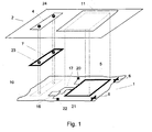
- Fig. 1 shows a first apparatus part 1 consisting of a substrate 10 on which a component 5 and an electrical connection 17, a pad 20 and distinctive marks 6 are laid out by a position reference system during the production of the apparatus part.
- the component 16, the electrical connection 21 and the pad 22 are secured to the apparatus part 1 by a positioning system during a further processing of the apparatus part.
- the positioning means 7 of the first apparatus part are shown with two stylised guiding means 23, designed to match the corresponding stylised guiding means 24 on the positioning means 4 of the second apparatus part 2 and to ensure the correct position of the apparatus part 1 relative to the second apparatus part 2 and the component 5 relative to the feature 11 in particular.
- Fig. 1 illustrates the basic idea of the invention, namely to utilise distinctive marks 6 added to an apparatus part 1 during its processing (by a reference positioning system) to position it precisely relative to another part or structure 2, e.g. in an apparatus.
- the distinctive marks 6 should have well defined geometrical relations to the 'decisive components' 5 or structural elements 17, 20 of the first apparatus part 1 (i.e. e.g. to its edges, to the boundaries of certain components of the part, to its electrical connections, etc.) which are to govern the position of the part 1 (and the component 5 in particular) relative to specific features 11 of the second apparatus part 2, to which it is to be joined. This information must be extracted from the reference positioning system and transferred to and used by the positioning system controlling the assembly process.
- the chosen distinctive mark(s) 6 of the first apparatus part may e.g.
- the positioning means 7 of the first apparatus part 1 may be located on the part with a known geometrical relationship to the fix-points and hence to the decisive components 5 or structural elements 17, 20 on the first apparatus part 1.
- the co-operating positioning means 4 on the second apparatus part 2 with which the first apparatus part 1 is to be joined may be designed and located on the second apparatus part to implement a desired position of the decisive components 5 or structural elements 17, 20 on the first apparatus part 1 relative to corresponding features 11 of the second apparatus part 2, when the co-operating positioning means 4, 7 are joined.
- the 'distinctive marks' 6 may be special alignment marks, electrical connections 17 or pads 20 for electrical connections, structural features of active or passive devices (e.g. gates of transistors, boundaries of capacitors) or other structures that are easy to identify for the positioning system used in the assembly process (including e.g. micro-mechanical features).
- a single distinctive mark 6 e.g. a cross or a circle
- Two separate distinctive marks 6 are required to fix the first apparatus part 1 to a second apparatus part 2 in two dimensions.
- the term 'the first apparatus part' 1 may cover a device consisting of a substrate 10 on which one or more components 5, 16 or other structural elements 17, 20 are integrated, possibly with connections 20 to the exterior and between them 17.
- An 'apparatus part' 1 may e.g. be a liquid crystal display module, a multi-chip-module (MCM), a micro-mechanical module, an integrated optics module, etc.
- the 'second apparatus part' 2 in relation to which the first apparatus part 1 is to be positioned (and joined) may be a special carrier (e.g. a light guide), a PCB, a housing member (including an outer housing member, e.g. a front cover, a frame, etc.), an identical apparatus part (enabling the cascading of identical parts), a guiding means for co-operating with corresponding receiving means on another device, etc.
- a special carrier e.g. a light guide
- a PCB e.g. a light guide
- a housing member including an outer housing member, e.g. a front cover, a frame, etc.
- an identical apparatus part enabling the cascading of identical parts
- a guiding means for co-operating with corresponding receiving means on another device etc.
- the 'substrate' 10 of the apparatus part 1 is taken to mean any carrier, e.g. a semiconductor substrate, a PCB, a glass or ceramic plate or the like.
- 'Components' 5, 16 may e.g. be the active parts of a display (e.g. of an LCD), integrated circuits (e.g. a driver circuit for a display), micro-mechanical devices, electro-optical devices, optical devices (e.g. laser diodes or photodiodes) or other functional bodies.
- a display e.g. of an LCD
- integrated circuits e.g. a driver circuit for a display
- micro-mechanical devices e.g. a driver circuit for a display
- electro-optical devices e.g. laser diodes or photodiodes
- optical devices e.g. laser diodes or photodiodes
- the term 'decisive components' refer to the components or component features that are to control the positioning of the first apparatus part relative to the second apparatus part.
- 'Structural elements' are taken to mean parts of a component that may be isolated due to their function or visual appearance or other functional features (e.g. electrical connections 17, 21 or other connections, including pads 20; 22).
- the structural elements 17, 20 may be added to the part 1 by means of the position reference system or another positioning system (in the latter case they are referred to as 21, 22).
- the 'position reference system' is the positioning system or systems (in case that more than one is used) used for the layout of the distinctive marks 6 and of the individual layers or steps that constitute the creation of or placement of the decisive components 5 and structural elements 17, 20 in the production process of the apparatus part 1.
- the 'positioning system' may be the position reference system or another positioning system having means for reading the relevant distinctive marks 6.
- the positioning system may be used to secure one or more components 16 or other structural elements 21, 22 to the apparatus part 1 (in addition to the ones laid out by the position reference system (possibly 5, 17, 20)).
- the positioning system may e.g. be a vision system used in the assembly process, where the first apparatus part 1 is joined with other apparatus parts 2.
- a 'vision system' is a pattern recognition system that enables automatic handling of known structures, e.g. by an assembly robot. The vision system must be able to read the relevant distinctive marks 6 on the apparatus part 1 and to use information from the position reference system as to the mutual relative positions of the distinctive marks 6 and the 'decisive components' 5 on the apparatus part 1.
- the positioning means 7 of the apparatus part 1 can be applied in the same operation and with the same accuracy as the components 5 or other structural elements in question and as the distinctive marks 6 of the part 1. This has the advantage of eliminating a link in the tolerance chain.
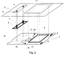
- Fig. 2 is identical to fig. 1 , except that the positioning means 7 of the first apparatus part 1 are shown with two protruding members 8. These members 8 are designed to match the corresponding apertures 9 on the receiving positioning means 4 of the second apparatus part 2 and to ensure the correct position of the first apparatus part 1 relative to the second apparatus part 2.
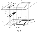
- Fig. 3 is identical to fig. 1 , except that the positioning means 7 of the first apparatus part 1 are shown with two apertures 18 that co-operate with the receiving means 4 of the second apparatus part 2 comprising a corresponding number of protruding members 19. These members 18 are designed to match the corresponding apertures 19 on the receiving positioning means 4 of the second apparatus part 2 and to ensure the correct position of the first apparatus part 1 relative to the second apparatus part 2.
- Figs. 4 and 5 show a preferred embodiment of the invention where the first apparatus part 1 is an LCD unit 101 (i.e. the 'decisive component' (5 in figs. 1-3 ) is the active display area 105 of the LCD) comprising a glass plate substrate 110 that is provided with a transparent print of an electrically conductive pattern controlling the visual output of the display. Also included on the first apparatus part is a driver circuit 116 for the LCD, the driver circuit being secured to the apparatus part 101 under control of a vision system using distinctive marks. The electrical connections (e.g. pads 120) may be used as distinctive marks.
- the positioning means 107 of the first apparatus part 101 are shown with two protruding members 108. These members 108 are designed to match the corresponding apertures (109 in fig.
- the positioning means 107 of the first apparatus part 101 include a receiving slot 14 for accommodating an elastomeric block 13 with a plurality of individually isolated conducting members 12 for establishing electrical contact between the first apparatus part 101 and a printed circuit board (115 in fig. 7 ).
- the positioning means 107 including means for establishing electrical contact to a PCB (115 in fig. 7 ), are mounted on the same side of the substrate 110 as the active display area 105. They might, however, also be mounted on the opposite side of the substrate 110 (as indicated in fig. 7 ).
- the distinctive marks 106 (or 120) on the LCD unit 101 have well-defined geometrical relations to the active area of the display 105 (i.e. to its boundaries), which is to control the position of the unit relative to the light guide (102 in fig. 6 and 7 ) (and in particular relative to its window (cf. 111 in fig. 6 )), to which it is to be joined. This information must be extracted from the reference positioning system used during the layout of the LCD unit 101 and transferred to and used by the vision system controlling the assembly process.
- the chosen distinctive marks 106; 120 of the LCD unit 101 are used by the assembly system as fix-points, and the positioning means 107 of the LCD unit 101 may be located on and secured to the LCD-substrate 110 with a known geometrical relationship to the active area of the display 105.
- the co-operating positioning means (109 in fig. 6 ) on the light guide (102 in fig. 6 ) may be designed and located on the light guide to implement a desired position of the active area 105 of the display unit 101 relative to the corresponding window (111 in fig. 6 ) of the light guide (102 in fig. 6 ), when the co-operating positioning means (108, 109) are joined.
- the positioning means 107 of the LCD unit 101 are secured to the unit 101 using glue.
- Other embodiments may be made, using adhesive tape, soldering or fastening by screws or the like.
- a light guide 102 for a mobile telephone (3 in fig. 7 ) is shown.
- This plate-shaped light guide 102 functions as a carrier for the LCD display unit 101.
- the light guide 102 is preferably made in a transparent plastics material and comprises a window area 111 and receiving guiding means 104 provided with two apertures 109 adjacent to the window area 111 for receiving and accurately positioning the guiding means (107, 108 in figs. 4 , 5 ) of the LCD display unit 101.
- the two apertures 109 in the light guide 102 are dimensioned and positioned such as to accommodate the correspondingly positioned and dimensioned protrusions 108 on the positioning means 107 of the display unit (101 in figs. 4 and 5 ). This ensures that the active area 105 of the display unit 101 is accurately positioned with respect to the corresponding window 111 of the light guide 102.
- the LCD unit 101 is secured to the light guide 102 simply by joining the protruding members (108 in fig. 4 , 5 ) of the positioning means 107 on the LCD unit 101 with the corresponding apertures 109 on the receiving positioning means 104 of the light guide 102.
- Other embodiments may be made, using other joining techniques (e.g. snap fasteners, fastening by screws, glue, adhesive tape, 'click-join', etc.) or combinations hereof.
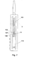
- FIG. 7 the mounting of an LCD display unit 101 in a mobile telephone 3 is shown.
- the LCD display unit 101 is positioned on a light guide 102 that is assembled to a printed circuit board (PCB) 115. This assembly is mounted in the front cover of the mobile phone 3.
- the LCD unit 101 is provided with positioning means 107 comprising protruding means 108, which are used for precision mounting the unit 101 to the light guide 102 by joining them with correspondingly positioned and dimensioned apertures (cf. 109 in fig. 6 ) in the light guide 102.
- Electrical connection between the LCD unit and the PCB 115 is achieved by an elastomeric block 13 with a plurality of individually isolated conducting members (12 in fig. 4 ).
- the 'apparatus' 3 in which the apparatus parts 1, 2; 101, 102 are mounted may be any apparatus in which the unique features of the method are required, including electronic devices, e.g. communications devices, among these mobile telephones, pagers, etc.
- the invention has been used in connection with the precision mounting of an LCD unit in a mobile telephone.
- the invention may, however, be used in all other cases where a precisely laid out first apparatus part is to be precision mounted on another apparatus part by using, in the assembly process, distinctive marks originating from the layout of the first apparatus part.
Landscapes
- Physics & Mathematics (AREA)
- Nonlinear Science (AREA)
- Optics & Photonics (AREA)
- Crystallography & Structural Chemistry (AREA)
- Chemical & Material Sciences (AREA)
- General Physics & Mathematics (AREA)
- Mathematical Physics (AREA)
- Devices For Indicating Variable Information By Combining Individual Elements (AREA)
- Liquid Crystal (AREA)
- Auxiliary Devices For And Details Of Packaging Control (AREA)
- Telephone Set Structure (AREA)
- Supply And Installment Of Electrical Components (AREA)
- Ropes Or Cables (AREA)
- Diaphragms For Electromechanical Transducers (AREA)
Applications Claiming Priority (3)
| Application Number | Priority Date | Filing Date | Title |
|---|---|---|---|
| SE9900584 | 1999-02-17 | ||
| SE9900584A SE516551C2 (sv) | 1999-02-17 | 1999-02-17 | Förfarande och anordning för precisionsmontering av en första apparatdel på en andra apparatdel |
| PCT/SE2000/000287 WO2000049847A1 (en) | 1999-02-17 | 2000-02-14 | A method for mounting an apparatus, an apparatus and an apparatus part |
Publications (2)
| Publication Number | Publication Date |
|---|---|
| EP1159859A1 EP1159859A1 (en) | 2001-12-05 |
| EP1159859B1 true EP1159859B1 (en) | 2009-03-04 |
Family
ID=20414543
Family Applications (1)
| Application Number | Title | Priority Date | Filing Date |
|---|---|---|---|
| EP00909847A Expired - Lifetime EP1159859B1 (en) | 1999-02-17 | 2000-02-14 | A method for mounting an apparatus, an apparatus and an apparatus part |
Country Status (11)
| Country | Link |
|---|---|
| US (1) | US6711386B1 (enExample) |
| EP (1) | EP1159859B1 (enExample) |
| JP (1) | JP2002537589A (enExample) |
| CN (1) | CN1197447C (enExample) |
| AT (1) | ATE424712T1 (enExample) |
| AU (1) | AU3202600A (enExample) |
| DE (1) | DE60041693D1 (enExample) |
| HK (1) | HK1045054B (enExample) |
| SE (1) | SE516551C2 (enExample) |
| TR (1) | TR200102359T2 (enExample) |
| WO (1) | WO2000049847A1 (enExample) |
Family Cites Families (12)
| Publication number | Priority date | Publication date | Assignee | Title |
|---|---|---|---|---|
| GB2146935B (en) * | 1983-08-18 | 1986-10-22 | Plessey Co Plc | Jigs for locating electrical components |
| US4651203A (en) * | 1985-10-29 | 1987-03-17 | At&T Technologies, Inc. | Video controlled article positioning system |
| TW278212B (enExample) * | 1992-05-06 | 1996-06-11 | Sumitomo Electric Industries | |
| JPH07115296A (ja) * | 1993-10-15 | 1995-05-02 | Sanyo Electric Co Ltd | 部品実装機の制御装置 |
| JPH0983093A (ja) * | 1995-09-18 | 1997-03-28 | Hitachi Ltd | プリント配線板 |
| FR2741505B1 (fr) * | 1995-11-20 | 1998-02-06 | Magneti Marelli France | Substrat electronique comprenant un pion d'indexation mecanique |
| US6347218B1 (en) * | 1996-02-28 | 2002-02-12 | Nokia Mobile Phones Limited | Electronic device with housing supplement |
| US5867772A (en) * | 1996-03-08 | 1999-02-02 | Ericsson, Inc. | Cellular telephone assembly and method for assembling a cellular telephone |
| JPH1051198A (ja) * | 1996-05-08 | 1998-02-20 | Tenryu Technic:Kk | 電子部品実装方法 |
| JP3139741B2 (ja) * | 1997-04-25 | 2001-03-05 | 日本電気株式会社 | 携帯無線情報端末装置 |
| JP4237834B2 (ja) * | 1997-06-03 | 2009-03-11 | 富士通株式会社 | 携帯電話機 |
| JPH11274966A (ja) * | 1998-03-19 | 1999-10-08 | Toshiba Corp | 携帯無線端末装置 |
-
1999
- 1999-02-17 SE SE9900584A patent/SE516551C2/sv not_active IP Right Cessation
-
2000
- 2000-02-14 WO PCT/SE2000/000287 patent/WO2000049847A1/en not_active Ceased
- 2000-02-14 AT AT00909847T patent/ATE424712T1/de not_active IP Right Cessation
- 2000-02-14 DE DE60041693T patent/DE60041693D1/de not_active Expired - Lifetime
- 2000-02-14 AU AU32026/00A patent/AU3202600A/en not_active Abandoned
- 2000-02-14 JP JP2000600464A patent/JP2002537589A/ja active Pending
- 2000-02-14 CN CNB008039216A patent/CN1197447C/zh not_active Expired - Fee Related
- 2000-02-14 EP EP00909847A patent/EP1159859B1/en not_active Expired - Lifetime
- 2000-02-14 HK HK02106645.4A patent/HK1045054B/zh not_active IP Right Cessation
- 2000-02-14 TR TR2001/02359T patent/TR200102359T2/xx unknown
- 2000-02-16 US US09/504,948 patent/US6711386B1/en not_active Expired - Lifetime
Also Published As
| Publication number | Publication date |
|---|---|
| CN1340292A (zh) | 2002-03-13 |
| JP2002537589A (ja) | 2002-11-05 |
| WO2000049847A1 (en) | 2000-08-24 |
| EP1159859A1 (en) | 2001-12-05 |
| TR200102359T2 (tr) | 2002-01-21 |
| SE9900584L (sv) | 2000-08-18 |
| AU3202600A (en) | 2000-09-04 |
| SE516551C2 (sv) | 2002-01-29 |
| ATE424712T1 (de) | 2009-03-15 |
| HK1045054B (zh) | 2005-11-04 |
| CN1197447C (zh) | 2005-04-13 |
| US6711386B1 (en) | 2004-03-23 |
| HK1045054A1 (en) | 2002-11-08 |
| SE9900584D0 (sv) | 1999-02-17 |
| DE60041693D1 (de) | 2009-04-16 |
Similar Documents
| Publication | Publication Date | Title |
|---|---|---|
| KR100464066B1 (ko) | 플렉시블 인쇄회로 및 배선기판을 상호접속하기 위한 구조및 방법과, 액정표시장치, 및 그 제조방법 | |
| US4116376A (en) | Method of mounting integrated circuit chips on a substrate and apparatus for carrying out the method | |
| US5982468A (en) | Liquid crystal display apparatus having dummy lead and dummy land for alignment | |
| EP1159859B1 (en) | A method for mounting an apparatus, an apparatus and an apparatus part | |
| KR100281394B1 (ko) | 평면표시장치 및 그 제조방법_ | |
| CN113238400B (zh) | 对位标记、显示装置和对位标记的判断方法 | |
| JPH09218420A (ja) | 液晶表示装置の製造方法 | |
| JP3018653B2 (ja) | 液晶表示モジュール | |
| CN1163782C (zh) | 显示装置、设有显示装置的设备及制造该显示装置的方法 | |
| CN217563879U (zh) | 芯片定位装置 | |
| MXPA01008048A (en) | A method for mounting an apparatus, an apparatus and an apparatus part | |
| JP4713720B2 (ja) | 液晶表示装置 | |
| CN216650392U (zh) | 摄像头组装定位系统 | |
| JP3792558B2 (ja) | 液晶装置の製造方法 | |
| JPS63152134A (ja) | 液晶表示装置 | |
| TWI292499B (enExample) | ||
| KR20000000652U (ko) | 플라즈마 디스플레이 패널 장치 | |
| JPH07281166A (ja) | 液晶表示素子 | |
| GB2246728A (en) | Support for a circuit board | |
| JPH05259660A (ja) | 部品の実装方法 | |
| JPH0820633B2 (ja) | 液晶表示装置 | |
| JP2000012995A (ja) | 回路基板に対する端子部品の取付け装置 | |
| JPH04116727U (ja) | 光学式エンコーダ |
Legal Events
| Date | Code | Title | Description |
|---|---|---|---|
| PUAI | Public reference made under article 153(3) epc to a published international application that has entered the european phase |
Free format text: ORIGINAL CODE: 0009012 |
|
| 17P | Request for examination filed |
Effective date: 20010810 |
|
| AK | Designated contracting states |
Kind code of ref document: A1 Designated state(s): AT BE CH CY DE DK ES FI FR GB GR IE IT LI LU MC NL PT SE |
|
| AX | Request for extension of the european patent |
Free format text: AL;LT;LV;MK;RO;SI |
|
| RAP1 | Party data changed (applicant data changed or rights of an application transferred) |
Owner name: TELEFONAKTIEBOLAGET LM ERICSSON (PUBL) |
|
| 17Q | First examination report despatched |
Effective date: 20071010 |
|
| GRAP | Despatch of communication of intention to grant a patent |
Free format text: ORIGINAL CODE: EPIDOSNIGR1 |
|
| GRAS | Grant fee paid |
Free format text: ORIGINAL CODE: EPIDOSNIGR3 |
|
| GRAA | (expected) grant |
Free format text: ORIGINAL CODE: 0009210 |
|
| AK | Designated contracting states |
Kind code of ref document: B1 Designated state(s): AT BE CH CY DE DK ES FI FR GB GR IE IT LI LU MC NL PT SE |
|
| REG | Reference to a national code |
Ref country code: GB Ref legal event code: FG4D |
|
| REG | Reference to a national code |
Ref country code: CH Ref legal event code: EP |
|
| REG | Reference to a national code |
Ref country code: IE Ref legal event code: FG4D |
|
| REF | Corresponds to: |
Ref document number: 60041693 Country of ref document: DE Date of ref document: 20090416 Kind code of ref document: P |
|
| PG25 | Lapsed in a contracting state [announced via postgrant information from national office to epo] |
Ref country code: NL Free format text: LAPSE BECAUSE OF FAILURE TO SUBMIT A TRANSLATION OF THE DESCRIPTION OR TO PAY THE FEE WITHIN THE PRESCRIBED TIME-LIMIT Effective date: 20090304 Ref country code: FI Free format text: LAPSE BECAUSE OF FAILURE TO SUBMIT A TRANSLATION OF THE DESCRIPTION OR TO PAY THE FEE WITHIN THE PRESCRIBED TIME-LIMIT Effective date: 20090304 |
|
| NLV1 | Nl: lapsed or annulled due to failure to fulfill the requirements of art. 29p and 29m of the patents act | ||
| PG25 | Lapsed in a contracting state [announced via postgrant information from national office to epo] |
Ref country code: SE Free format text: LAPSE BECAUSE OF FAILURE TO SUBMIT A TRANSLATION OF THE DESCRIPTION OR TO PAY THE FEE WITHIN THE PRESCRIBED TIME-LIMIT Effective date: 20090604 Ref country code: AT Free format text: LAPSE BECAUSE OF FAILURE TO SUBMIT A TRANSLATION OF THE DESCRIPTION OR TO PAY THE FEE WITHIN THE PRESCRIBED TIME-LIMIT Effective date: 20090304 |
|
| PG25 | Lapsed in a contracting state [announced via postgrant information from national office to epo] |
Ref country code: BE Free format text: LAPSE BECAUSE OF FAILURE TO SUBMIT A TRANSLATION OF THE DESCRIPTION OR TO PAY THE FEE WITHIN THE PRESCRIBED TIME-LIMIT Effective date: 20090304 |
|
| PG25 | Lapsed in a contracting state [announced via postgrant information from national office to epo] |
Ref country code: ES Free format text: LAPSE BECAUSE OF FAILURE TO SUBMIT A TRANSLATION OF THE DESCRIPTION OR TO PAY THE FEE WITHIN THE PRESCRIBED TIME-LIMIT Effective date: 20090615 Ref country code: PT Free format text: LAPSE BECAUSE OF FAILURE TO SUBMIT A TRANSLATION OF THE DESCRIPTION OR TO PAY THE FEE WITHIN THE PRESCRIBED TIME-LIMIT Effective date: 20090818 |
|
| PLBE | No opposition filed within time limit |
Free format text: ORIGINAL CODE: 0009261 |
|
| STAA | Information on the status of an ep patent application or granted ep patent |
Free format text: STATUS: NO OPPOSITION FILED WITHIN TIME LIMIT |
|
| PG25 | Lapsed in a contracting state [announced via postgrant information from national office to epo] |
Ref country code: DK Free format text: LAPSE BECAUSE OF FAILURE TO SUBMIT A TRANSLATION OF THE DESCRIPTION OR TO PAY THE FEE WITHIN THE PRESCRIBED TIME-LIMIT Effective date: 20090304 |
|
| 26N | No opposition filed |
Effective date: 20091207 |
|
| REG | Reference to a national code |
Ref country code: CH Ref legal event code: PL |
|
| PG25 | Lapsed in a contracting state [announced via postgrant information from national office to epo] |
Ref country code: MC Free format text: LAPSE BECAUSE OF NON-PAYMENT OF DUE FEES Effective date: 20100301 Ref country code: GR Free format text: LAPSE BECAUSE OF FAILURE TO SUBMIT A TRANSLATION OF THE DESCRIPTION OR TO PAY THE FEE WITHIN THE PRESCRIBED TIME-LIMIT Effective date: 20090605 Ref country code: CH Free format text: LAPSE BECAUSE OF NON-PAYMENT OF DUE FEES Effective date: 20100228 Ref country code: LI Free format text: LAPSE BECAUSE OF NON-PAYMENT OF DUE FEES Effective date: 20100228 |
|
| REG | Reference to a national code |
Ref country code: FR Ref legal event code: ST Effective date: 20101029 |
|
| PG25 | Lapsed in a contracting state [announced via postgrant information from national office to epo] |
Ref country code: FR Free format text: LAPSE BECAUSE OF NON-PAYMENT OF DUE FEES Effective date: 20100301 Ref country code: IE Free format text: LAPSE BECAUSE OF NON-PAYMENT OF DUE FEES Effective date: 20100214 |
|
| PG25 | Lapsed in a contracting state [announced via postgrant information from national office to epo] |
Ref country code: CY Free format text: LAPSE BECAUSE OF FAILURE TO SUBMIT A TRANSLATION OF THE DESCRIPTION OR TO PAY THE FEE WITHIN THE PRESCRIBED TIME-LIMIT Effective date: 20090304 |
|
| PG25 | Lapsed in a contracting state [announced via postgrant information from national office to epo] |
Ref country code: LU Free format text: LAPSE BECAUSE OF NON-PAYMENT OF DUE FEES Effective date: 20100214 |
|
| PGFP | Annual fee paid to national office [announced via postgrant information from national office to epo] |
Ref country code: DE Payment date: 20180227 Year of fee payment: 19 Ref country code: GB Payment date: 20180227 Year of fee payment: 19 |
|
| PGFP | Annual fee paid to national office [announced via postgrant information from national office to epo] |
Ref country code: IT Payment date: 20180222 Year of fee payment: 19 |
|
| REG | Reference to a national code |
Ref country code: DE Ref legal event code: R119 Ref document number: 60041693 Country of ref document: DE |
|
| GBPC | Gb: european patent ceased through non-payment of renewal fee |
Effective date: 20190214 |
|
| PG25 | Lapsed in a contracting state [announced via postgrant information from national office to epo] |
Ref country code: GB Free format text: LAPSE BECAUSE OF NON-PAYMENT OF DUE FEES Effective date: 20190214 Ref country code: DE Free format text: LAPSE BECAUSE OF NON-PAYMENT OF DUE FEES Effective date: 20190903 |
|
| PG25 | Lapsed in a contracting state [announced via postgrant information from national office to epo] |
Ref country code: IT Free format text: LAPSE BECAUSE OF NON-PAYMENT OF DUE FEES Effective date: 20190214 |