EP1159767B1 - Verfahren zum vergüten eines supraleitermaterials mit hoher remanenzinduktion und dessen verwendung - Google Patents
Verfahren zum vergüten eines supraleitermaterials mit hoher remanenzinduktion und dessen verwendung Download PDFInfo
- Publication number
- EP1159767B1 EP1159767B1 EP99973753A EP99973753A EP1159767B1 EP 1159767 B1 EP1159767 B1 EP 1159767B1 EP 99973753 A EP99973753 A EP 99973753A EP 99973753 A EP99973753 A EP 99973753A EP 1159767 B1 EP1159767 B1 EP 1159767B1
- Authority
- EP
- European Patent Office
- Prior art keywords
- shaped body
- coating
- superconducting
- coating material
- process according
- Prior art date
- Legal status (The legal status is an assumption and is not a legal conclusion. Google has not performed a legal analysis and makes no representation as to the accuracy of the status listed.)
- Expired - Lifetime
Links
- 239000000463 material Substances 0.000 title claims abstract description 165
- 238000000034 method Methods 0.000 title claims abstract description 77
- 238000000576 coating method Methods 0.000 title claims abstract description 54
- 239000011248 coating agent Substances 0.000 title claims abstract description 53
- 230000006698 induction Effects 0.000 title claims abstract description 26
- 239000002887 superconductor Substances 0.000 title claims description 19
- 238000012986 modification Methods 0.000 claims abstract description 19
- 230000004048 modification Effects 0.000 claims abstract description 19
- 238000001816 cooling Methods 0.000 claims abstract description 17
- 229910052727 yttrium Inorganic materials 0.000 claims abstract description 17
- QVGXLLKOCUKJST-UHFFFAOYSA-N atomic oxygen Chemical compound [O] QVGXLLKOCUKJST-UHFFFAOYSA-N 0.000 claims abstract description 15
- 238000010438 heat treatment Methods 0.000 claims abstract description 15
- 229910052760 oxygen Inorganic materials 0.000 claims abstract description 15
- 239000001301 oxygen Substances 0.000 claims abstract description 15
- 230000009969 flowable effect Effects 0.000 claims abstract description 14
- 229910052761 rare earth metal Inorganic materials 0.000 claims abstract description 13
- 229910052746 lanthanum Inorganic materials 0.000 claims abstract description 11
- 229910052769 Ytterbium Inorganic materials 0.000 claims abstract description 8
- 229910052684 Cerium Inorganic materials 0.000 claims abstract description 6
- 229910052692 Dysprosium Inorganic materials 0.000 claims abstract description 6
- 229910052779 Neodymium Inorganic materials 0.000 claims abstract description 6
- 229910052777 Praseodymium Inorganic materials 0.000 claims abstract description 6
- 229910052693 Europium Inorganic materials 0.000 claims abstract description 5
- 229910052688 Gadolinium Inorganic materials 0.000 claims abstract description 5
- -1 Er Tm Inorganic materials 0.000 claims abstract description 4
- 229910052765 Lutetium Inorganic materials 0.000 claims abstract description 4
- 229910052771 Terbium Inorganic materials 0.000 claims abstract description 4
- 239000000155 melt Substances 0.000 claims abstract description 3
- 230000008569 process Effects 0.000 claims description 44
- 239000010949 copper Substances 0.000 claims description 41
- 239000000203 mixture Substances 0.000 claims description 19
- 239000013078 crystal Substances 0.000 claims description 14
- 238000002844 melting Methods 0.000 claims description 13
- 230000008018 melting Effects 0.000 claims description 13
- 239000000843 powder Substances 0.000 claims description 8
- VWQVUPCCIRVNHF-UHFFFAOYSA-N yttrium atom Chemical compound [Y] VWQVUPCCIRVNHF-UHFFFAOYSA-N 0.000 claims description 8
- FZLIPJUXYLNCLC-UHFFFAOYSA-N lanthanum atom Chemical compound [La] FZLIPJUXYLNCLC-UHFFFAOYSA-N 0.000 claims description 7
- 229910052802 copper Inorganic materials 0.000 claims description 5
- 239000007789 gas Substances 0.000 claims description 5
- 239000002245 particle Substances 0.000 claims description 5
- 239000000126 substance Substances 0.000 claims description 5
- RYGMFSIKBFXOCR-UHFFFAOYSA-N Copper Chemical compound [Cu] RYGMFSIKBFXOCR-UHFFFAOYSA-N 0.000 claims description 4
- 229910052772 Samarium Inorganic materials 0.000 claims description 4
- 229910052791 calcium Inorganic materials 0.000 claims description 4
- 239000011575 calcium Substances 0.000 claims description 4
- 229910052729 chemical element Inorganic materials 0.000 claims description 4
- 238000004519 manufacturing process Methods 0.000 claims description 4
- 239000007787 solid Substances 0.000 claims description 4
- 229910052775 Thulium Inorganic materials 0.000 claims description 3
- 229910052788 barium Inorganic materials 0.000 claims description 3
- DSAJWYNOEDNPEQ-UHFFFAOYSA-N barium atom Chemical compound [Ba] DSAJWYNOEDNPEQ-UHFFFAOYSA-N 0.000 claims description 3
- 150000001768 cations Chemical class 0.000 claims description 3
- OYPRJOBELJOOCE-UHFFFAOYSA-N Calcium Chemical compound [Ca] OYPRJOBELJOOCE-UHFFFAOYSA-N 0.000 claims description 2
- 239000000443 aerosol Substances 0.000 claims description 2
- 229910052790 beryllium Inorganic materials 0.000 claims description 2
- 229910052797 bismuth Inorganic materials 0.000 claims description 2
- 229910052793 cadmium Inorganic materials 0.000 claims description 2
- 229910052737 gold Inorganic materials 0.000 claims description 2
- 239000008187 granular material Substances 0.000 claims description 2
- 229910052735 hafnium Inorganic materials 0.000 claims description 2
- 229910052741 iridium Inorganic materials 0.000 claims description 2
- 229910052747 lanthanoid Inorganic materials 0.000 claims description 2
- 150000002602 lanthanoids Chemical class 0.000 claims description 2
- 229910052745 lead Inorganic materials 0.000 claims description 2
- 229910052749 magnesium Inorganic materials 0.000 claims description 2
- 229910052762 osmium Inorganic materials 0.000 claims description 2
- 229910052763 palladium Inorganic materials 0.000 claims description 2
- 229910052697 platinum Inorganic materials 0.000 claims description 2
- 238000001556 precipitation Methods 0.000 claims description 2
- 229910052706 scandium Inorganic materials 0.000 claims description 2
- 229910052709 silver Inorganic materials 0.000 claims description 2
- 238000005118 spray pyrolysis Methods 0.000 claims description 2
- 238000005507 spraying Methods 0.000 claims description 2
- 238000003860 storage Methods 0.000 claims description 2
- 229910052712 strontium Inorganic materials 0.000 claims description 2
- 229910052717 sulfur Inorganic materials 0.000 claims description 2
- 229910052725 zinc Inorganic materials 0.000 claims description 2
- 229910052726 zirconium Inorganic materials 0.000 claims description 2
- 229910019020 PtO2 Inorganic materials 0.000 claims 1
- YKIOKAURTKXMSB-UHFFFAOYSA-N adams's catalyst Chemical compound O=[Pt]=O YKIOKAURTKXMSB-UHFFFAOYSA-N 0.000 claims 1
- CETPSERCERDGAM-UHFFFAOYSA-N ceric oxide Chemical compound O=[Ce]=O CETPSERCERDGAM-UHFFFAOYSA-N 0.000 claims 1
- 229910000422 cerium(IV) oxide Inorganic materials 0.000 claims 1
- 238000009792 diffusion process Methods 0.000 claims 1
- 238000010309 melting process Methods 0.000 claims 1
- 238000012216 screening Methods 0.000 claims 1
- 239000000725 suspension Substances 0.000 claims 1
- 229910052689 Holmium Inorganic materials 0.000 abstract description 3
- 238000000465 moulding Methods 0.000 description 41
- 230000005381 magnetic domain Effects 0.000 description 14
- 239000002243 precursor Substances 0.000 description 12
- 239000000523 sample Substances 0.000 description 12
- 238000009826 distribution Methods 0.000 description 11
- 238000005259 measurement Methods 0.000 description 9
- 230000007547 defect Effects 0.000 description 7
- 230000008595 infiltration Effects 0.000 description 5
- 238000001764 infiltration Methods 0.000 description 5
- 230000006911 nucleation Effects 0.000 description 5
- 238000010899 nucleation Methods 0.000 description 5
- 238000005496 tempering Methods 0.000 description 5
- 229910052691 Erbium Inorganic materials 0.000 description 4
- 230000004907 flux Effects 0.000 description 4
- 238000005339 levitation Methods 0.000 description 4
- 238000002360 preparation method Methods 0.000 description 4
- 238000012545 processing Methods 0.000 description 4
- 229910002480 Cu-O Inorganic materials 0.000 description 3
- 230000008901 benefit Effects 0.000 description 3
- 230000008859 change Effects 0.000 description 3
- 238000000227 grinding Methods 0.000 description 3
- 230000005415 magnetization Effects 0.000 description 3
- 238000010583 slow cooling Methods 0.000 description 3
- 238000012360 testing method Methods 0.000 description 3
- 238000011282 treatment Methods 0.000 description 3
- IJGRMHOSHXDMSA-UHFFFAOYSA-N Atomic nitrogen Chemical compound N#N IJGRMHOSHXDMSA-UHFFFAOYSA-N 0.000 description 2
- 244000052616 bacterial pathogen Species 0.000 description 2
- 230000015572 biosynthetic process Effects 0.000 description 2
- 238000006243 chemical reaction Methods 0.000 description 2
- 238000010276 construction Methods 0.000 description 2
- 238000002425 crystallisation Methods 0.000 description 2
- 230000008025 crystallization Effects 0.000 description 2
- 238000011161 development Methods 0.000 description 2
- 230000018109 developmental process Effects 0.000 description 2
- 238000010304 firing Methods 0.000 description 2
- 238000009434 installation Methods 0.000 description 2
- 238000005498 polishing Methods 0.000 description 2
- 239000004810 polytetrafluoroethylene Substances 0.000 description 2
- 229920001343 polytetrafluoroethylene Polymers 0.000 description 2
- 239000011148 porous material Substances 0.000 description 2
- 238000004544 sputter deposition Methods 0.000 description 2
- 230000007704 transition Effects 0.000 description 2
- 229910021521 yttrium barium copper oxide Inorganic materials 0.000 description 2
- QNRATNLHPGXHMA-XZHTYLCXSA-N (r)-(6-ethoxyquinolin-4-yl)-[(2s,4s,5r)-5-ethyl-1-azabicyclo[2.2.2]octan-2-yl]methanol;hydrochloride Chemical compound Cl.C([C@H]([C@H](C1)CC)C2)CN1[C@@H]2[C@H](O)C1=CC=NC2=CC=C(OCC)C=C21 QNRATNLHPGXHMA-XZHTYLCXSA-N 0.000 description 1
- 229910018072 Al 2 O 3 Inorganic materials 0.000 description 1
- BQCADISMDOOEFD-UHFFFAOYSA-N Silver Chemical compound [Ag] BQCADISMDOOEFD-UHFFFAOYSA-N 0.000 description 1
- 238000007545 Vickers hardness test Methods 0.000 description 1
- 238000004026 adhesive bonding Methods 0.000 description 1
- 238000000137 annealing Methods 0.000 description 1
- 239000011449 brick Substances 0.000 description 1
- 229910052799 carbon Inorganic materials 0.000 description 1
- 150000004649 carbonic acid derivatives Chemical class 0.000 description 1
- GWXLDORMOJMVQZ-UHFFFAOYSA-N cerium Chemical compound [Ce] GWXLDORMOJMVQZ-UHFFFAOYSA-N 0.000 description 1
- 150000001860 citric acid derivatives Chemical class 0.000 description 1
- RKTYLMNFRDHKIL-UHFFFAOYSA-N copper;5,10,15,20-tetraphenylporphyrin-22,24-diide Chemical compound [Cu+2].C1=CC(C(=C2C=CC([N-]2)=C(C=2C=CC=CC=2)C=2C=CC(N=2)=C(C=2C=CC=CC=2)C2=CC=C3[N-]2)C=2C=CC=CC=2)=NC1=C3C1=CC=CC=C1 RKTYLMNFRDHKIL-UHFFFAOYSA-N 0.000 description 1
- 238000005336 cracking Methods 0.000 description 1
- 238000000354 decomposition reaction Methods 0.000 description 1
- 230000002950 deficient Effects 0.000 description 1
- 238000000151 deposition Methods 0.000 description 1
- 230000008021 deposition Effects 0.000 description 1
- 238000013461 design Methods 0.000 description 1
- 238000011156 evaluation Methods 0.000 description 1
- 230000008020 evaporation Effects 0.000 description 1
- 238000001704 evaporation Methods 0.000 description 1
- 150000002222 fluorine compounds Chemical class 0.000 description 1
- 230000035784 germination Effects 0.000 description 1
- 150000004820 halides Chemical class 0.000 description 1
- 230000035876 healing Effects 0.000 description 1
- 238000000265 homogenisation Methods 0.000 description 1
- 150000004679 hydroxides Chemical class 0.000 description 1
- 238000003780 insertion Methods 0.000 description 1
- 230000037431 insertion Effects 0.000 description 1
- 238000005304 joining Methods 0.000 description 1
- 238000000608 laser ablation Methods 0.000 description 1
- 239000007788 liquid Substances 0.000 description 1
- 238000000691 measurement method Methods 0.000 description 1
- 238000011326 mechanical measurement Methods 0.000 description 1
- 150000002823 nitrates Chemical class 0.000 description 1
- 229910052757 nitrogen Inorganic materials 0.000 description 1
- 210000001331 nose Anatomy 0.000 description 1
- 238000005457 optimization Methods 0.000 description 1
- 150000003891 oxalate salts Chemical class 0.000 description 1
- 238000006213 oxygenation reaction Methods 0.000 description 1
- 238000005240 physical vapour deposition Methods 0.000 description 1
- 238000003825 pressing Methods 0.000 description 1
- 230000001681 protective effect Effects 0.000 description 1
- 230000009467 reduction Effects 0.000 description 1
- 229910000938 samarium–cobalt magnet Inorganic materials 0.000 description 1
- 239000004332 silver Substances 0.000 description 1
- 238000005245 sintering Methods 0.000 description 1
- 238000003980 solgel method Methods 0.000 description 1
- 241000894007 species Species 0.000 description 1
- 229910001220 stainless steel Inorganic materials 0.000 description 1
- 239000010935 stainless steel Substances 0.000 description 1
- 239000007858 starting material Substances 0.000 description 1
- 238000006467 substitution reaction Methods 0.000 description 1
- 238000004781 supercooling Methods 0.000 description 1
- 229920003002 synthetic resin Polymers 0.000 description 1
- 239000000057 synthetic resin Substances 0.000 description 1
- 229910052716 thallium Inorganic materials 0.000 description 1
- 238000012546 transfer Methods 0.000 description 1
- 238000007740 vapor deposition Methods 0.000 description 1
- 238000004857 zone melting Methods 0.000 description 1
Images

Classifications
-
- H—ELECTRICITY
- H10—SEMICONDUCTOR DEVICES; ELECTRIC SOLID-STATE DEVICES NOT OTHERWISE PROVIDED FOR
- H10N—ELECTRIC SOLID-STATE DEVICES NOT OTHERWISE PROVIDED FOR
- H10N60/00—Superconducting devices
- H10N60/01—Manufacture or treatment
-
- H—ELECTRICITY
- H10—SEMICONDUCTOR DEVICES; ELECTRIC SOLID-STATE DEVICES NOT OTHERWISE PROVIDED FOR
- H10N—ELECTRIC SOLID-STATE DEVICES NOT OTHERWISE PROVIDED FOR
- H10N60/00—Superconducting devices
- H10N60/01—Manufacture or treatment
- H10N60/0268—Manufacture or treatment of devices comprising copper oxide
- H10N60/0661—Processes performed after copper oxide formation, e.g. patterning
Definitions
- the invention relates to a method for tempering a superconducting material, the quenched, only one grain or a few grains or one or more magnetic domains containing superconducting material based on (Y / SE) BaCuO with high material properties, in particular with high remanence, and the use of the tempered material.
- the goal is to produce the highest possible superconducting and magnetic properties.
- Particular advantages arise when textured polycrystalline or only one or a few magnetic domains having superconducting materials are used. The best are the magnetic properties when the molding has only one magnetic domain.
- a high-temperature superconducting molded body is located above its transition temperature T c in the field of a permanent magnet, it is penetrated by a magnetic flux. If the superconductor is cooled to temperatures below the critical temperature, part of the magnetic flux in the superconductor material remains frozen. A shift of the high-temperature superconducting molded body is possible in this state only under application of force. The stability of such a bearing is the greater, the more magnetic flux can be frozen in the superconducting material, that is, the higher the maximum value of the remanent induction.
- Improved magnetic properties e.g. higher values of remanence induction and levitation force, e.g. the construction of magnetic bearings with a larger gap between the superconducting components and the permanent or electromagnet.
- larger imbalances or deviations from the ideal running of the rotors are allowed.
- storage of the flywheel in Schwungmassenspeichem on such camps can be increased by increasing the gap, the safety reserves and simpler, technically and economically less complex to be constructed bearing geometries are accepted.
- One way of increasing the remanent induction of such a shaped article can be to enlarge the magnetic domains by processing larger one-dimensional shaped articles.
- the growth front in shaped bodies based on (Y / SE) BaCuO with largely homogeneous starting composition becomes unstable with increasing size of the grains.
- An enlargement of the magnetic domains without enlarging the moldings can also be achieved in moldings provided with cracks and / or other defects by the healing of such defects according to the method described in the German patent application 198 41 925.2 (corresponding to WO 00/15581 ) can be achieved.
- EP 1011153 A2 (A document according to Article 54 (3) EPC) describes an oxidic superconductor and a process for its preparation, wherein the superconductor is impregnated with a synthetic resin layer.
- the object is achieved with a method for tempering shaped bodies made of a superconducting material based on SEBaCuO with SE at least one rare earth element including lanthanum and yttrium, which is characterized in that a coating of a coating material is applied to at least a portion of a region of a surface of the shaped body wherein the application material at least partially melts at a lower temperature than the molded body material and / or is flowable at a lower temperature than that material and optionally flows out on the surface of the shaped body, wherein the shaped body is heated with the applied application material to a temperature, wherein the molded body material is not yet melted and / or not yet flowable, but wherein the application material is in the at least partially melted and / or flowable state, and wherein at least a portion of a near-surface region of the Fo Body is modified at this temperature and / or subsequent cooling by the application material completely or partially infiltrated at least the near-surface region of the shaped body, and in which
- Cooling and / or enriched in a subsequent heat treatment with oxygen wherein the modification contributes to increase the remanent induction and / or the critical current density of the oxygen-enriched molded body, and wherein the application material at least one rare earth element selected from the group consisting of Y, La , Ce, Pr, Nd, Eu, Gd, Tb, Dy, Ho, Er, Tm, Yb and Lu, and at least one alkaline earth element, copper and oxygen.
- the superconducting material contains at least one superconducting or superconducting phase, the superconductive phase becoming oxygenated to a superconducting phase when appropriately oxygenated. It preferably contains at least one rare earth element (including lanthanum and yttrium) as well as at least barium, copper and oxygen and optionally also elements from the group of Be, Mg, Ca, Sr, Zn, Cd, Sc, Zr, Hf, Pt, Pd, Os , Ir, Ru, Ag, Cu, Au, Hg, Ag, Tl, Pb, Bi and S.
- the trivalent elements serve preferably as a replacement of yttrium and the bivalent preferably for modulating the electronic structure or for partial replacement of barium.
- Rare earth elements SE in the sense of this application also include lanthanum and yttrium.
- rare earth elements Y, La, Ce, Nd, Sm, Pr, Eu, Gd, Yb, Dy, Er are preferable, with Ce, Pr and Sm being preferred only as a proportion of mixed crystals besides other rare earth elements.
- Cerium can be used to refine the particles of the 211 phase and similar pinning centers. Particularly preferred are Y, Yb, Dy, Er and Nd.
- a material of the molded article or / and a coating material is selected from the group of materials based on Y-Ea-Cu-O, SE-Ea-Cu-O, SE-Ea-Cu-O, wherein shares of these chemical elements by others unsubstituted and wherein Ea is at least one alkaline earth element.
- Suitable high-temperature superconducting materials for the process according to the invention are those in which the superconductor material of the shaped body to be modified or modified and / or the application material contains phases which are selected from the group of phases having an approximate composition of Y 1 Ba 2 Cu 3 O v , Y 2 Ba 1 Cu 1 O w , Yb 1 Ba 2 Cu 3 O v ' , Yb 2 Ba 1 Cu 1 O w' , Sm 1 Ba 2 Cu 3 O v " , Sm 2 Ba 1 Cu 1 O w " Nd 1 Ba 2 Cu 3 O v"' , Nd 4 Ba 2 Cu 2 O w "' , Dy 1 Ba 2 Cu 3 O v”” , Dy 2 Ba 1 Cu 1 O w "" , He 1 Ba 2 Cu 3 O v ""' , He 2 Ba 1 Cu 1 O w ""' , Eu 1 Ba 2 Cu 3 O w "”” , Eu 2 Ba 1 Cu 1 O w “”” , Gd 1 Ba 2 Cu 3
- the untreated or / and the treated shaped body of the superconducting material, the coating material and / or the layer material may additionally comprise calcium and / or other cations which alter the band structure of the electrons and contribute to higher critical transport stream densities.
- the shaped body of the superconducting material and / or the application material may also have at least one gradient with regard to the chemical composition, the structure or / and the peritectic, flow or melting temperature.
- the magnetic domains do not necessarily correspond to regions of aligned magnetic moments, as is the case with permanent magnets, but are applied according to the conditions of the magnetization used Field oriented.
- the magnetic domains are referred to hereinafter in this application only as "domains".
- the aim of the further development and optimization of such moldings is to produce the highest possible values of the remanence induction and the critical transport stream density, which allows the use of smaller modified moldings according to the invention for the same technical application. If the shaped body after texturing has an inhomogeneous distribution of superconducting properties, in particular towards the edge areas, then the shaped body is to be modified more strongly or in a special way, in particular in the edge area, in order to achieve a homogenization of the distribution of the superconducting properties.
- Moldings as precursor material for the process according to the invention which are provided with only one grain or with a few grains or with only one magnetic domain or with few magnetic domains, are preferably used in a modified melt texture growth process such as e.g. the melt-textured-growth method, in a top-seeded-melt-growth method with an overhead seed, in a zone melting process such as the vertical gradient freeze method, or in a single crystal growing method, such as e.g. produced by the modified Bridgeman process. Moldings made in one of these processes sometimes have only one to six magnetic domains. If such samples have cracks or / and contaminated or structurally disturbed areas, these defects can be filled in and / or healed, and also the split magnetic domains can be annealed.
- a modified melt texture growth process such as e.g. the melt-textured-growth method, in a top-seeded-melt-growth method with an overhead seed, in a zone melting process such as the vertical gradient freeze method, or in a single crystal growing method, such as
- an enrichment with oxygen can be carried out, especially with a slow cooling in the temperature range of about 500 to 350 ° C or at a holding time in this temperature range using a flowing oxygen-rich gas stream. Otherwise, the shaped body after texturing must be enriched with oxygen in at least one further heat treatment.
- the microstructure of the moldings produced in this way is formed from one or more grains. These grains in turn are composed of plates separated by small-angle grain boundaries of less than 1 °.
- spherical or acicular particles of phase 211 having diameters of about 100 nm to about 100 ⁇ m are distributed throughout the shaped body. The following describes the characteristic process steps and features of the main texturing processes:
- This process is a non-directional texturing process without spatial temperature gradients.
- the texturing is carried out mainly by slow cooling of the molding from the partially molten state to temperatures below the peritectic or melting temperature.
- VFG Vertical gradient freeze method
- This process is a directed melt texturing process.
- An off of e.g. eight individually controllable zones built stationary oven is controlled so that a temperature profile is passed through the also held stationary sample.
- the vertical temperature gradient may be e.g. 25 K / cm.
- In the area of the peritectic temperature or melting temperature is often cooled at about 1 K / h.
- the resulting melt-textured shaped bodies contain in the first molten area due to the random nucleation several grains.
- grains whose c-axes are aligned substantially parallel to the temperature gradient prevailing in the production process prevail.
- the orientation difference between such preferably growing grains can be up to about 15 °.
- the sample may preferably be moved vertically in relation to a stationary, often three-zone oven.
- the sample may be prepared either by a suitable underlay construction such as e.g. be supported by a crucible or hung on a pulling device.
- the temperature of the upper zone is typically typically about 850 ° C, the middle one about 1150 ° C, and the lower zone about 750 ° C.
- a gradient of, for example, about 20 K / cm is produced, through which the sample is conveyed at a speed of e.g. 1 mm / h can be passed. This then corresponds to a cooling rate of about 2 K / h.
- the cylindrical samples are often about 12 cm long and often have a diameter of about 6 mm. Below a 2 to 3 cm long nucleation zone, in the differently oriented grains compete in growth, the samples are usually einomänig and then inevitably have only one grain.
- the c-axis in this one-domain region is often inclined at about 45 ° to the sample axis.
- This method enables the preparation of crystallographically single-domain shaped bodies having a crystallographic orientation that can be dictated by the orientation of the appropriate seed crystal (seed) to be applied to the surface of the precursor material.
- the seed crystal must consist of a material which is still in crystalline form even at temperatures above the peritectic or melting temperature of the material to be textured.
- the lattice parameters of the seed material must approximate those of the material to be textured.
- the application of the seed can be carried out prior to the actual texturing step by pressing, sintering or simply by placing and during the texturing process by placing on the already heated sample.
- the thus seeded precursor material is converted to a partially molten state and rapidly cooled to a temperature below the peritectic or melting temperature of the material being textured, nucleation and growth in particular of the SE 1 Ba phase grains in direct contact with the seed crystal 2 Cu 3 O 7-x , the supercooling in other areas of the shaped body for the nucleation and grain growth is not sufficient.
- a holding time in the temperature profile is often chosen to stabilize the growth of the central grain.
- the subsequent temperature control must aim to dissipate the heat of crystallization which results and to obtain the stable growth of the central grain and to suppress the growth of further grains. This can be achieved by a sufficiently slow cooling and / or the insertion of further holding times.
- the samples thus prepared consist of a single grain with an orientation substantially equal to that given by the seed crystal.
- an orientation of the c-axis perpendicular to one of the surfaces of the geometry of the shaped body is preferred.
- the substructure of these grains is formed, as in the other processes for forming a precursor material, essentially from plate-like grains separated by small-angle comrades of less than 1 °.
- the superconducting properties, such as remanent induction, levitation force and / or height of the above-obtained shaped bodies as precursor material for the inventive tempering process can be improved by modifying the surface of the shaped body with the method of tempering described below.
- a coating material is applied to the molded body, which at least partially expires during the fire and possibly even spreads on the surface of the molded body.
- a superconducting material for the selection of the material of a nucleus, a superconducting material, a coating material, which can be on fire in the layer material or chemically identical to this, and a layer material results in the following temperature sequence, where T is the respective peritectic or melting temperature is meant and the use of a seed only serves to produce a suitable precursor material for the inventive tempering process T seed material > T superconducting material > T layer material -
- Table 1 basically provides guidelines for selecting the appropriate pairings of elements. However, mixtures of different elements, the use of pressure or negative pressure, contents of substances which lower the melting point or the peritectic temperature, and in particular the partial pressure of oxygen may cause a significant change in temperature and possibly also a change in the order listed in Table 1.
- the table does not take into account that the superconductor material may have a slightly different composition and different properties before treatment with a germ than after germination. Again, only the modification of the superconductor material with the layer material according to the invention.
- the application material is preferably applied in a layer thickness in the range of 1 .mu.m and 5 mm, more preferably in the range of 10 .mu.m to 3 mm, most preferably in the range of 50 .mu.m and 2 mm.
- a powder, a shaped body and / or a coating can be applied; as molding preferably a pressed, calcined, sintered or melted, possibly textured or melt-textured shaped body and as coating preferably a physically or / and chemically deposited, essentially by precipitation, decomposition reaction, spraying or spray pyrolysis produced coating such as laser ablation, gas phase deposition, sputtering , Vapor deposition, sputtering, CVD, PVD, sol-gel method.
- oxides, hydroxides, carbonates, nitrates and similar precursor materials such as citrates and oxalates can be used, but also materials for melting point reduction such as halides, in particular fluorides.
- materials for melting point reduction such as halides, in particular fluorides.
- the application material has a lower melting point or peritectic point than the superconducting material to be modified, which is why an addition is recommended with which the melting point can be lowered or the peritectic temperature can be lowered.
- a powdered coating material which also includes a single-phase or multi-phase powder, a powder mixture or / and granules, can i.a. be spread or struck; a shaped body of the coating material can be placed on the corresponding surface of the shaped body of the superconducting material or glued; e.g. from the gas phase or with an aerosol, the coating of the shaped body to be modified can be made.
- the coated shaped body of the superconductor material can be kept at a temperature at which the molded body material is not yet melted or / and is not flowable, but wherein the application material in at least partially melted and / or flowable state and wherein at least a portion of a Near-surface region of the molding is modified at this temperature and / or a subsequent cooling, so that a part of the coating material can diffuse or penetrate into the superconductor material to be modified.
- Surface defects e.g. Pores, cracks and micro-cracks, which may be present in the surface area to be modified, are closed and can be a solid interlocking by chemical or physicochemical reactions occur at the interfaces.
- certain elements can also diffuse deeper into the superconducting material to be modified.
- the order material may u.U. largely diffuse in, penetrate and, if necessary, subordinate evaporation, so that with thinner coatings possibly only a very thin residual layer or no remaining layer remains on the modified molding after firing.
- a gradient can be generated on the one hand in the shaped body of the superconductor material and / or on the other hand in the layer material produced from the application material, e.g. as a gradient of a particular element, which may also gradually influence the properties of the material.
- the layer material which in the form of a very shallow trained Pyramid-grown crystal surfaces or / and the unevenness of the formed body are then preferably mechanically removed, for example by sawing, grinding, lapping and / or polishing, and optionally subsequently subjected to a heat treatment, which can serve for oxygenation and / or annealing of the material.
- the shaped body to be modified preferably has a relative density of at least 80%, more preferably of at least 95%, but in exceptional cases, even less dense shaped bodies can offer advantages if they are treated according to the invention.
- the shaped body of the superconducting material can be set during the firing and heat treatments so that it is only in direct contact with a material based on SEBaCuO except for the application material, preferably with a material based on Y 2 BaCuO 5 . This helps to avoid contact reactions and partial deliquescence of the superconducting shaped body during the fire or the occurrence of mechanical stresses. Refractory bricks and kiln furniture based on MgO or Al 2 O 3 are therefore less suitable.
- the cooling after or during the modification of the superconducting material and after a subsequent heat treatment takes place as slowly as possible in order to avoid the formation of cracks, microcracks and flaking.
- the molded article may be oxygenated during cooling and / or during a re-heat treatment to produce and / or improve the superconducting properties.
- the modification of the superconducting material can lead to the formation of defects in the crystal lattice of the molded body, which contribute to the increase of the magnetic properties. This may be point defects, especially defects due to the installation of large or too small cations in the usually tetragonal Perovskite crystal lattice, voids, grain boundaries act, but it can also change the pore structure.
- a possibly existing crack, a grain boundary and / or a contaminated or structurally disturbed one can Area are removed, in particular by sawing, the remote area is treated thereafter in the further inventive method analogous to an area to be modified.
- This makes it possible, inter alia, completely heal defective moldings and modify or produce particularly large moldings with better properties than currently technically possible.
- the inventive method can be carried out in an advantageous manner so that the flowable coating material at high temperature at least partially penetrates into a crack and / or in a removed example by saw cut area of the molding, which are present in the surface area to be modified.
- the shaped body of the superconductor before modification and heat treatment on only one to a hundred grains or / and one to a hundred domains in order to reduce the number of grains or domains as possible to one to eight in the modification and optionally in the subsequent heat treatments ,
- the shaped body of the superconductor material has only one to a hundred grains and / or one to one hundred domains, in particular up to 50, particularly preferably only one to 20, very particularly preferably only one to eight grains or Domains or even just a grain and up to four domains.
- a large-sized shaped body of the superconducting material may have a plurality of spaced apart germs, the crystal orientations of the c-axes advantageously either substantially parallel to one of the Nauptraumen the geometry of the shaped body, for example, substantially parallel to the cylinder axis of a cylinder, or substantially perpendicular thereto ,
- the crystal orientation in the shaped body to be modified can be controlled.
- a large-sized shaped body of the superconducting material can advantageously be produced in several segments, which may be matched or even better joined together.
- the joining can be carried out in particular by heat treatment at a temperature at which the shaped body material is not yet melted and / or not flowable, but wherein the application material is in the at least partially melted and / or flowable state and wherein at least a portion of a near-surface Area of the molding is modified at this temperature and / or a subsequent cooling - optionally under pressure and optionally with the addition of a coating material on the interfaces to be joined together, but also, for example by a simple gluing.
- a mean roughness value R a of a certain size or as functional surfaces a specific shape of the Abbot support curve, or whose geometry requires certain dimensions of lengths, angles and / or shape and position tolerances such as flatness or Parallelism should be maintained
- the shaped body is mechanically reworked after cooling, eg by grinding, lapping, polishing and / or drums. It may also be useful to provide sharp edges by grinding with a chamfer or rounding or by drum with a rounding.
- shaped bodies of a superconducting material based on SEBaCuO with SE leave at least one rare earth element selected from the group consisting of Y, La, Ce, Pr, Nd, Eu, Gd, Tb, Dy, Ho, Er, Tm, Yb and Lu, which may have a high maximum value of remanence induction at 77K and 0T.
- the shaped body is a cylinder, a ring, a tube or a disc consisting essentially of one or more segments, the one Alignment of the c-axes of the grains or the one grain has substantially in the direction of the cylinder axis / plate axis or another main direction of the shaped body or perpendicular to it.
- the shaped body may substantially have a composition of SE 1 Ba 2 Cu 3 O x with x in the range of 6.5 to 7, wherein SE may occur in excess.
- it has more than 60% by volume, particularly preferably more than 70% or more than 80% by volume, of a phase of the composition SE 1 Ba 2 Cu 3 O x with x in the range from 6.5 to 7 on.
- the proportion of the 211 phase is too small, the superconducting properties may deteriorate.
- the shaped article may have a critical transport stream density of at least 4 ⁇ 10 4 A / cm 2 in the external field of 1 T at 77 K, preferably of at least 6x 10 4 A / cm 2 , more preferably of at least 8x10 4 A / cm 2 and in particular of at least 9.7 x 10 4 A / cm 2 . It may also have a fracture toughness determined from the cracking system having hardness impressions of at least 1 MPa ⁇ ⁇ m, preferably at least 1.5 MPa ⁇ m. Further, it may have a flexural strength of at least 300 MPa, preferably at least 400 MPa.
- the moldings produced according to the invention can be used for example for transformers, circuit breakers, power supply lines, magnetic shields, magnetic bearings and / or as magnets for different purposes.
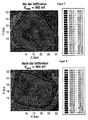
- FIGS. 1 and 3 give the measurement results of the precursor material and Figures 2 and 4 the measurement results of erfingdungshiel tempered superconducting material again.
- the superconducting molded body to be magnetized was placed at temperatures above its critical temperature in the field of a conventional electromagnet.
- the magnetic field penetrated fully into the non-superconducting shaped body in this state.
- the superconducting molded body was cooled below its transition temperature T c , usually to about 77 K, and then completely shut down the field of the electromagnet.
- T c transition temperature
- Part of the magnetic flux, the remanence induction remained frozen in the superconductor.
- the measurement of the distribution of this remanence induction was carried out by scanning the molding surface by means of a HHP-VA micro-sonic probe from Arepoc. The active area of the probe was usable down to a temperature of 4.2K. The measurements were usually performed only at 77K.
- the micro-sonic probe To protect the micro-sonic probe from contact with the mold surface during the measurement, it was kept submerged in a PTFE fixture. As a result, the minimum distance of the probe to the molding surface was 0.3 mm in the measurement. With this distance, the maximum value of the remanence induction was determined. The scanning of the shaped body surface for the determination of the distribution of the Remanzindutation was performed with a distance of 0.5 mm.
- the PTFE holder was connected to a 3D positioning system via a stainless steel rod.
- the control unit of the 3D positioning system was a C116-4 CNC controller from Isel, which could be controlled from a PC via an RS 232 interface.
- the stepper motors could be reproducibly positioned with a minimum increment of 10 ⁇ m.
- the maximum travel in X and Y direction was 32 cm, in the Z direction 28 cm.
- a permanent magnet was lowered from 100 mm height in steps of 0.5 mm on the surface of the molded body cooled to 77 K and moved back to its original position.
- the magnet used was according to standardization of the Technical Committee "superconducting materials" of the German Society for Materials (DGM) a cylindrical SmCo magnet with a diameter of 25 mm, a height of 15 mm and a remanence at the surface B z (0) of 0 , 4 T.
- the positioning was carried out using the positioning system described in the method for measuring the remanence induction. For the PC-based data acquisition, the mechanical measurement variable force was converted into an electrical measurement.
- strain gauge sensor strain gauge KAP-S 0.05 Fa. AST Dresden GmbH was used. This sensor was operated with the maximum possible voltage of 10 V; the permissible limit force was 150 N. The reading of the measuring data of the sensor was carried out via a digital multimeter, which could be read by the PC via an RS 232 interface.
- the fracture toughness could be measured by evaluating the crack pattern produced by a Vickers hardness test specimen.
- the length and configuration of the cracks resulting from the hardness test were related to the test load used and the hardness of the material.
- the hardness impressions were generated with a Leitz Durimed 2 small-diameter hardness tester with loads between 10 g and 500 g with a residence time of the test specimen on the surface of 15 s.
- the evaluation of the crack systems was carried out with a scanning electron microscope.
- the critical transport stream densities were determined by the conventional four-point method.
- currents of up to 400 A are conducted through the sample (cross-sectional area 0.25 mm 2 ) for a pulse duration of 1 ms.
- low-resistance silver contacts (0.04 mOhm) were burnt into the sample
- a shaped body of the composition Y 1 Ba 2 Cu 3 O 7-x which additionally contained 25 mol% of Y 2 O 3 and 1 wt.% CeO 2 , was heated at temperatures of up to 1045 ° C. by means of a melt-growth process with the seed sitting above ( top-seeded-melt-growth TSMG).
- the microstructure consisted of YBCO 123 with a high density of finest particles of YBCO 211.
- the dimensions of the finished textured plate-shaped molding were 34 x 34 x 12 mm.
- the molded article had no near-surface macroscopic cracks after texturing.
- the remanence induction distribution measured after texturing gave a maximum value of remanence induction B z, max of 820 mT ( FIG. 1 ), The conical geometry of this distribution shows the magnetic Eindomäntechnik of the molding.
- Example 2 It was prepared as in Example 1, a textured molding with dimensions 38x38x12 mm 3 . Unlike in Example 1, Er-123 was used as the coating material. The remanence induction distribution measured after texturing gave a maximum value of the remanent induction B z, max of 902 mT ( Figur3 ).
Landscapes
- Engineering & Computer Science (AREA)
- Manufacturing & Machinery (AREA)
- Inorganic Compounds Of Heavy Metals (AREA)
- Superconductors And Manufacturing Methods Therefor (AREA)
- Superconductor Devices And Manufacturing Methods Thereof (AREA)
- Oxygen, Ozone, And Oxides In General (AREA)
- Electrical Discharge Machining, Electrochemical Machining, And Combined Machining (AREA)
- Hard Magnetic Materials (AREA)
Applications Claiming Priority (3)
| Application Number | Priority Date | Filing Date | Title |
|---|---|---|---|
| DE19908597 | 1999-02-27 | ||
| DE19908597A DE19908597A1 (de) | 1999-02-27 | 1999-02-27 | Verfahren zum Vergüten eines Supraleitermaterials mit hoher Remanenzinduktion, vergütetes Supraleitermaterial und dessen Verwendung |
| PCT/EP1999/006680 WO2000052768A1 (de) | 1999-02-27 | 1999-09-10 | Verfahren zum vergüten eines supraleitermaterials mit hoher remanenzinduktion, vergütetes supraleitermaterial und dessen verwendung |
Publications (2)
| Publication Number | Publication Date |
|---|---|
| EP1159767A1 EP1159767A1 (de) | 2001-12-05 |
| EP1159767B1 true EP1159767B1 (de) | 2008-10-29 |
Family
ID=7899117
Family Applications (1)
| Application Number | Title | Priority Date | Filing Date |
|---|---|---|---|
| EP99973753A Expired - Lifetime EP1159767B1 (de) | 1999-02-27 | 1999-09-10 | Verfahren zum vergüten eines supraleitermaterials mit hoher remanenzinduktion und dessen verwendung |
Country Status (11)
| Country | Link |
|---|---|
| US (2) | US6830839B1 (enExample) |
| EP (1) | EP1159767B1 (enExample) |
| JP (1) | JP2002538071A (enExample) |
| KR (1) | KR100684224B1 (enExample) |
| CN (1) | CN1201413C (enExample) |
| AT (1) | ATE412979T1 (enExample) |
| CA (1) | CA2365437C (enExample) |
| DE (2) | DE19908597A1 (enExample) |
| DK (1) | DK1159767T3 (enExample) |
| NO (1) | NO20014121L (enExample) |
| WO (1) | WO2000052768A1 (enExample) |
Families Citing this family (7)
| Publication number | Priority date | Publication date | Assignee | Title |
|---|---|---|---|---|
| US6686827B2 (en) * | 2001-03-28 | 2004-02-03 | Protectronics Technology Corporation | Surface mountable laminated circuit protection device and method of making the same |
| DE10132522A1 (de) * | 2001-07-10 | 2003-02-13 | Zentrum Fuer Funktionswerkstof | Verfahren zum Ankeimen von Formkörpern aus einem Supraleitermaterial durch Einbetten eines Impfkristalls |
| JP5243800B2 (ja) * | 2004-12-23 | 2013-07-24 | スーパーコンダクター・テクノロジーズ・インコーポレイテッド | RF特性最適化(RE)Ba2Cu3O7−δ超伝導薄膜物品 |
| KR100753468B1 (ko) * | 2005-03-11 | 2007-08-31 | 삼성전기주식회사 | 배선 재료, 배선 기판 및 배선 기판의 형성방법 |
| US20070052304A1 (en) * | 2005-09-07 | 2007-03-08 | Philippe Masson | Multi-pattern high temperature superconducting motor using flux trapping and concentration |
| CA2792268C (en) * | 2010-03-10 | 2018-09-18 | Jrb Engineering Pty Ltd | Method and apparatus for magnetic crack depth prediction |
| CN108083799A (zh) * | 2017-12-21 | 2018-05-29 | 叶芳 | 一种新能源用超导材料及其制备方法 |
Family Cites Families (14)
| Publication number | Priority date | Publication date | Assignee | Title |
|---|---|---|---|---|
| FR2605451B1 (fr) * | 1986-10-17 | 1993-12-24 | Thomson Cgr | Aimant permanent cylindrique a champ induit longitudinal |
| FR2660107B1 (fr) * | 1990-03-22 | 1994-07-29 | Centre Nat Rech Scient | Procede de preparation d'un corps magnetique oriente et texture. |
| WO1991019029A1 (fr) * | 1990-06-07 | 1991-12-12 | Nippon Steel Corporation | Supraconducteur a oxyde et procede de production associe |
| JP2550253B2 (ja) * | 1990-12-14 | 1996-11-06 | 新日本製鐵株式会社 | 酸化物高温超電導体の製造方法 |
| JPH07106906B2 (ja) * | 1990-04-13 | 1995-11-15 | 新日本製鐵株式会社 | 希土類元素を含む酸化物超電導材料およびその製造方法 |
| JP2556401B2 (ja) * | 1990-06-07 | 1996-11-20 | 新日本製鐵株式会社 | 酸化物超電導体およびその製造方法 |
| JP2556401Y2 (ja) * | 1991-06-11 | 1997-12-03 | 三浦工業株式会社 | 給湯配管の腐食防止装置 |
| JP2838742B2 (ja) * | 1991-12-20 | 1998-12-16 | 新日本製鐵株式会社 | 酸化物バルク超電導体およびその製造方法 |
| US5325002A (en) * | 1992-02-18 | 1994-06-28 | Electric Power Research Institute | Trapped-field, superconducting, induction-synchronous motor/generator having improved startup torque |
| US5563564A (en) * | 1993-04-22 | 1996-10-08 | University Of Houston | Strong high-temperature superconductor trapped field magnets |
| US5821598A (en) * | 1995-02-01 | 1998-10-13 | Research Corporation Technologies, Inc. | Uncooled amorphous YBaCuO thin film infrared detector |
| JP3881732B2 (ja) * | 1996-10-16 | 2007-02-14 | 財団法人国際超電導産業技術研究センター | 酸化物超電導体複合体の製造方法 |
| US6083885A (en) * | 1997-01-14 | 2000-07-04 | Weinstein; Roy | Method of forming textured high-temperature superconductors |
| US6060433A (en) * | 1998-01-26 | 2000-05-09 | Nz Applied Technologies Corporation | Method of making a microwave device having a polycrystalline ferrite substrate |
-
1999
- 1999-02-27 DE DE19908597A patent/DE19908597A1/de not_active Ceased
- 1999-09-10 EP EP99973753A patent/EP1159767B1/de not_active Expired - Lifetime
- 1999-09-10 AT AT99973753T patent/ATE412979T1/de not_active IP Right Cessation
- 1999-09-10 KR KR1020017010962A patent/KR100684224B1/ko not_active Expired - Fee Related
- 1999-09-10 DK DK99973753T patent/DK1159767T3/da active
- 1999-09-10 CA CA002365437A patent/CA2365437C/en not_active Expired - Fee Related
- 1999-09-10 CN CNB998163694A patent/CN1201413C/zh not_active Expired - Fee Related
- 1999-09-10 JP JP2000603103A patent/JP2002538071A/ja active Pending
- 1999-09-10 US US09/914,156 patent/US6830839B1/en not_active Expired - Fee Related
- 1999-09-10 WO PCT/EP1999/006680 patent/WO2000052768A1/de not_active Ceased
- 1999-09-10 DE DE59914891T patent/DE59914891D1/de not_active Expired - Lifetime
-
2001
- 2001-08-24 NO NO20014121A patent/NO20014121L/no unknown
-
2003
- 2003-09-25 US US10/669,650 patent/US20040058823A1/en not_active Abandoned
Also Published As
| Publication number | Publication date |
|---|---|
| EP1159767A1 (de) | 2001-12-05 |
| CA2365437C (en) | 2008-07-08 |
| NO20014121D0 (no) | 2001-08-24 |
| DE19908597A1 (de) | 2000-09-14 |
| CA2365437A1 (en) | 2000-09-08 |
| WO2000052768A1 (de) | 2000-09-08 |
| KR20020001746A (ko) | 2002-01-09 |
| ATE412979T1 (de) | 2008-11-15 |
| CN1338122A (zh) | 2002-02-27 |
| JP2002538071A (ja) | 2002-11-12 |
| CN1201413C (zh) | 2005-05-11 |
| US20040058823A1 (en) | 2004-03-25 |
| NO20014121L (no) | 2001-08-24 |
| DK1159767T3 (da) | 2009-03-09 |
| US6830839B1 (en) | 2004-12-14 |
| KR100684224B1 (ko) | 2007-02-20 |
| DE59914891D1 (de) | 2008-12-11 |
Similar Documents
| Publication | Publication Date | Title |
|---|---|---|
| DE3887478T2 (de) | Methode zur Herstellung eines Oxid-Supraleiters. | |
| DE3889024T2 (de) | Verfahren zum Herstellen einer supraleitenden Dünnschicht. | |
| DE69012731T2 (de) | Oxydsupraleiter und verfahren zur herstellung. | |
| DE68911455T2 (de) | Verfahren zum Herstellen eines Oxid-Supraleiters vom Bismut-Typ. | |
| DE69209856T2 (de) | Supraleitendes Oxidmaterial und Verfahren zu seiner Herstellung | |
| EP1159767B1 (de) | Verfahren zum vergüten eines supraleitermaterials mit hoher remanenzinduktion und dessen verwendung | |
| DE60224418T2 (de) | Methode zum verbinden von supraleitern und ein verbundsupraleiter | |
| EP1157429B1 (de) | Supraleitende körper aus zinkdotiertem kupferoxidmaterial | |
| US5434125A (en) | Rare earth oxide superconducting material and process for producing the same | |
| DE3853900T2 (de) | Supraleitendes Material und Verfahren zu seiner Herstellung. | |
| DE19750598A1 (de) | Erzeugnis mit einem Substrat aus einem teilstabilisierten Zirkonoxid und einer Pufferschicht aus einem vollstabilisierten Zirkonoxid sowie Verfahren zu seiner Herstellung | |
| DE9318197U1 (de) | Hochtemperatur Supraleiter Material | |
| DE69032641T2 (de) | Verfahren zur Herstellung eines oxidischen Supraleiters | |
| DE3854493T2 (de) | Verfahren zur Herstellung eines Dünnschichtsupraleiters. | |
| DE3855357T2 (de) | Verfahren zur Herstellung von supraleitenden Keramiken | |
| DE19623050C2 (de) | Verfahren zur Herstellung hochtemperatursupraleitender, schmelztexturierter massiver Materialien | |
| DE68925187T2 (de) | Supraleitende Dickschicht-Leiterplatte, deren Herstellung, Dickschicht-Supraleiter und dessen Herstellung | |
| DE3887765T2 (de) | Verfahren zur Herstellung einer dicken supraleitenden Schicht. | |
| DE19748743C1 (de) | Verfahren zur Herstellung von schmelztexturierten Volumenproben auf der Basis der Hochtemperatursupraleiter Sm¶1¶Ba¶2¶Cu¶3¶O¶7¶(Sm-123) | |
| DE19708711C1 (de) | Verfahren zur Züchtung von Einkristallen von Hochtemperatursupraleitern aus Seltenerd-Kupraten der Form SE¶1¶¶+¶¶x¶Ba¶2¶¶-¶¶x¶Cu¶3¶0¶7¶¶-¶¶delta¶ und nach dem Verfahren hergestellte Kristalle | |
| DE19748742C1 (de) | Verfahren zur Herstellung von schmelztexturierten Volumenproben auf der Basis der Hochtemperatursupraleiter Nd¶1¶Ba¶2¶Cu¶3¶O¶7¶(Nd-123) | |
| DE19817875C2 (de) | Verfahren zur Herstellung von optimierten, schmelztexturierten Volumenproben auf der Basis des Hochtemperatursupraleiters Y¶1¶Ba¶2¶Cu¶3¶O¶7¶ | |
| EP1115677A1 (de) | Verfahren zum ausheilen von rissen in keramischen formkörpern und derart behandelte formkörper | |
| DE10132522A1 (de) | Verfahren zum Ankeimen von Formkörpern aus einem Supraleitermaterial durch Einbetten eines Impfkristalls | |
| DE19841575A1 (de) | Verfahren zur Herstellung schmelztexturierter Volumenproben auf der Basis des Hochtemperatursupraleiters Sm¶1¶Ba¶2¶Cu¶3¶O¶7¶/Sm¶2¶Ba¶1¶Cu¶1¶O¶5¶ (SmBC) |
Legal Events
| Date | Code | Title | Description |
|---|---|---|---|
| PUAI | Public reference made under article 153(3) epc to a published international application that has entered the european phase |
Free format text: ORIGINAL CODE: 0009012 |
|
| 17P | Request for examination filed |
Effective date: 20010912 |
|
| AK | Designated contracting states |
Kind code of ref document: A1 Designated state(s): AT BE CH CY DE DK ES FI FR GB GR IE IT LI LU MC NL PT SE |
|
| 17Q | First examination report despatched |
Effective date: 20041206 |
|
| 17Q | First examination report despatched |
Effective date: 20041206 |
|
| RTI1 | Title (correction) |
Free format text: METHOD FOR COATING A SEMICONDUCTOR MATERIAL USING HIGH REMANENT INDUCTION AND THE USE THEREOF |
|
| GRAP | Despatch of communication of intention to grant a patent |
Free format text: ORIGINAL CODE: EPIDOSNIGR1 |
|
| RTI1 | Title (correction) |
Free format text: METHOD FOR COATING A SUPERCONDUCTOR MATERIAL HAVING HIGH REMANENT INDUCTION AND THE USE THEREOF |
|
| GRAS | Grant fee paid |
Free format text: ORIGINAL CODE: EPIDOSNIGR3 |
|
| GRAA | (expected) grant |
Free format text: ORIGINAL CODE: 0009210 |
|
| AK | Designated contracting states |
Kind code of ref document: B1 Designated state(s): AT BE CH CY DE DK ES FI FR GB GR IE IT LI LU MC NL PT SE |
|
| REG | Reference to a national code |
Ref country code: GB Ref legal event code: FG4D Free format text: NOT ENGLISH |
|
| REG | Reference to a national code |
Ref country code: CH Ref legal event code: EP |
|
| REG | Reference to a national code |
Ref country code: IE Ref legal event code: FG4D Free format text: LANGUAGE OF EP DOCUMENT: GERMAN |
|
| REF | Corresponds to: |
Ref document number: 59914891 Country of ref document: DE Date of ref document: 20081211 Kind code of ref document: P |
|
| REG | Reference to a national code |
Ref country code: SE Ref legal event code: TRGR |
|
| REG | Reference to a national code |
Ref country code: DK Ref legal event code: T3 |
|
| PG25 | Lapsed in a contracting state [announced via postgrant information from national office to epo] |
Ref country code: ES Free format text: LAPSE BECAUSE OF FAILURE TO SUBMIT A TRANSLATION OF THE DESCRIPTION OR TO PAY THE FEE WITHIN THE PRESCRIBED TIME-LIMIT Effective date: 20090209 |
|
| PG25 | Lapsed in a contracting state [announced via postgrant information from national office to epo] |
Ref country code: PT Free format text: LAPSE BECAUSE OF FAILURE TO SUBMIT A TRANSLATION OF THE DESCRIPTION OR TO PAY THE FEE WITHIN THE PRESCRIBED TIME-LIMIT Effective date: 20090330 Ref country code: FI Free format text: LAPSE BECAUSE OF FAILURE TO SUBMIT A TRANSLATION OF THE DESCRIPTION OR TO PAY THE FEE WITHIN THE PRESCRIBED TIME-LIMIT Effective date: 20081029 |
|
| REG | Reference to a national code |
Ref country code: IE Ref legal event code: FD4D |
|
| PG25 | Lapsed in a contracting state [announced via postgrant information from national office to epo] |
Ref country code: IE Free format text: LAPSE BECAUSE OF FAILURE TO SUBMIT A TRANSLATION OF THE DESCRIPTION OR TO PAY THE FEE WITHIN THE PRESCRIBED TIME-LIMIT Effective date: 20081029 |
|
| PLBE | No opposition filed within time limit |
Free format text: ORIGINAL CODE: 0009261 |
|
| STAA | Information on the status of an ep patent application or granted ep patent |
Free format text: STATUS: NO OPPOSITION FILED WITHIN TIME LIMIT |
|
| 26N | No opposition filed |
Effective date: 20090730 |
|
| PGFP | Annual fee paid to national office [announced via postgrant information from national office to epo] |
Ref country code: DK Payment date: 20090910 Year of fee payment: 11 |
|
| PGFP | Annual fee paid to national office [announced via postgrant information from national office to epo] |
Ref country code: SE Payment date: 20090915 Year of fee payment: 11 Ref country code: NL Payment date: 20090915 Year of fee payment: 11 Ref country code: GB Payment date: 20090922 Year of fee payment: 11 Ref country code: CH Payment date: 20090923 Year of fee payment: 11 |
|
| PGFP | Annual fee paid to national office [announced via postgrant information from national office to epo] |
Ref country code: DE Payment date: 20090922 Year of fee payment: 11 |
|
| BERE | Be: lapsed |
Owner name: NEXANS SUPERCONDUCTORS G.M.B.H. Effective date: 20090930 |
|
| PG25 | Lapsed in a contracting state [announced via postgrant information from national office to epo] |
Ref country code: MC Free format text: LAPSE BECAUSE OF NON-PAYMENT OF DUE FEES Effective date: 20090930 |
|
| PGFP | Annual fee paid to national office [announced via postgrant information from national office to epo] |
Ref country code: IT Payment date: 20090925 Year of fee payment: 11 |
|
| PG25 | Lapsed in a contracting state [announced via postgrant information from national office to epo] |
Ref country code: BE Free format text: LAPSE BECAUSE OF NON-PAYMENT OF DUE FEES Effective date: 20090930 |
|
| PG25 | Lapsed in a contracting state [announced via postgrant information from national office to epo] |
Ref country code: GR Free format text: LAPSE BECAUSE OF FAILURE TO SUBMIT A TRANSLATION OF THE DESCRIPTION OR TO PAY THE FEE WITHIN THE PRESCRIBED TIME-LIMIT Effective date: 20090130 |
|
| PG25 | Lapsed in a contracting state [announced via postgrant information from national office to epo] |
Ref country code: AT Free format text: LAPSE BECAUSE OF NON-PAYMENT OF DUE FEES Effective date: 20090910 |
|
| REG | Reference to a national code |
Ref country code: NL Ref legal event code: V1 Effective date: 20110401 |
|
| PG25 | Lapsed in a contracting state [announced via postgrant information from national office to epo] |
Ref country code: LU Free format text: LAPSE BECAUSE OF NON-PAYMENT OF DUE FEES Effective date: 20090910 |
|
| REG | Reference to a national code |
Ref country code: CH Ref legal event code: PL |
|
| REG | Reference to a national code |
Ref country code: SE Ref legal event code: EUG |
|
| GBPC | Gb: european patent ceased through non-payment of renewal fee |
Effective date: 20100910 |
|
| REG | Reference to a national code |
Ref country code: DK Ref legal event code: EBP |
|
| PG25 | Lapsed in a contracting state [announced via postgrant information from national office to epo] |
Ref country code: IT Free format text: LAPSE BECAUSE OF NON-PAYMENT OF DUE FEES Effective date: 20100910 |
|
| REG | Reference to a national code |
Ref country code: FR Ref legal event code: ST Effective date: 20110531 |
|
| REG | Reference to a national code |
Ref country code: DE Ref legal event code: R119 Ref document number: 59914891 Country of ref document: DE Effective date: 20110401 |
|
| PG25 | Lapsed in a contracting state [announced via postgrant information from national office to epo] |
Ref country code: LI Free format text: LAPSE BECAUSE OF NON-PAYMENT OF DUE FEES Effective date: 20100930 Ref country code: DE Free format text: LAPSE BECAUSE OF NON-PAYMENT OF DUE FEES Effective date: 20110401 Ref country code: CH Free format text: LAPSE BECAUSE OF NON-PAYMENT OF DUE FEES Effective date: 20100930 Ref country code: FR Free format text: LAPSE BECAUSE OF NON-PAYMENT OF DUE FEES Effective date: 20100930 |
|
| PG25 | Lapsed in a contracting state [announced via postgrant information from national office to epo] |
Ref country code: NL Free format text: LAPSE BECAUSE OF NON-PAYMENT OF DUE FEES Effective date: 20110401 Ref country code: GB Free format text: LAPSE BECAUSE OF NON-PAYMENT OF DUE FEES Effective date: 20100910 |
|
| PG25 | Lapsed in a contracting state [announced via postgrant information from national office to epo] |
Ref country code: CY Free format text: LAPSE BECAUSE OF FAILURE TO SUBMIT A TRANSLATION OF THE DESCRIPTION OR TO PAY THE FEE WITHIN THE PRESCRIBED TIME-LIMIT Effective date: 20081029 |
|
| PGFP | Annual fee paid to national office [announced via postgrant information from national office to epo] |
Ref country code: FR Payment date: 20091001 Year of fee payment: 11 |
|
| PG25 | Lapsed in a contracting state [announced via postgrant information from national office to epo] |
Ref country code: DK Free format text: LAPSE BECAUSE OF NON-PAYMENT OF DUE FEES Effective date: 20100930 |
|
| PG25 | Lapsed in a contracting state [announced via postgrant information from national office to epo] |
Ref country code: SE Free format text: LAPSE BECAUSE OF NON-PAYMENT OF DUE FEES Effective date: 20100911 |