EP1158584A2 - Semiconductor device having semiconductor resistance element and fabrication method thereof - Google Patents
Semiconductor device having semiconductor resistance element and fabrication method thereof Download PDFInfo
- Publication number
- EP1158584A2 EP1158584A2 EP01112470A EP01112470A EP1158584A2 EP 1158584 A2 EP1158584 A2 EP 1158584A2 EP 01112470 A EP01112470 A EP 01112470A EP 01112470 A EP01112470 A EP 01112470A EP 1158584 A2 EP1158584 A2 EP 1158584A2
- Authority
- EP
- European Patent Office
- Prior art keywords
- region
- semiconductor
- substrate
- type
- semiconductor resistance
- Prior art date
- Legal status (The legal status is an assumption and is not a legal conclusion. Google has not performed a legal analysis and makes no representation as to the accuracy of the status listed.)
- Granted
Links
- 239000004065 semiconductor Substances 0.000 title claims abstract description 163
- 238000004519 manufacturing process Methods 0.000 title claims description 11
- 238000000034 method Methods 0.000 title description 22
- 239000000758 substrate Substances 0.000 claims abstract description 74
- 150000001875 compounds Chemical class 0.000 claims abstract description 22
- 239000012535 impurity Substances 0.000 claims description 51
- 230000000694 effects Effects 0.000 abstract description 12
- 239000010410 layer Substances 0.000 description 75
- 229920002120 photoresistant polymer Polymers 0.000 description 25
- 239000002184 metal Substances 0.000 description 15
- 238000000605 extraction Methods 0.000 description 13
- 230000001681 protective effect Effects 0.000 description 10
- 150000002500 ions Chemical class 0.000 description 6
- 238000000206 photolithography Methods 0.000 description 6
- 238000005468 ion implantation Methods 0.000 description 5
- 229910001218 Gallium arsenide Inorganic materials 0.000 description 4
- 238000005268 plasma chemical vapour deposition Methods 0.000 description 4
- 238000002513 implantation Methods 0.000 description 3
- 239000011241 protective layer Substances 0.000 description 3
- 238000005019 vapor deposition process Methods 0.000 description 3
- KRHYYFGTRYWZRS-UHFFFAOYSA-N Fluorane Chemical compound F KRHYYFGTRYWZRS-UHFFFAOYSA-N 0.000 description 2
- -1 GaAs compound Chemical class 0.000 description 2
- 238000000137 annealing Methods 0.000 description 2
- RBFQJDQYXXHULB-UHFFFAOYSA-N arsane Chemical compound [AsH3] RBFQJDQYXXHULB-UHFFFAOYSA-N 0.000 description 2
- 239000011248 coating agent Substances 0.000 description 2
- 238000000576 coating method Methods 0.000 description 2
- 230000006866 deterioration Effects 0.000 description 2
- 239000007789 gas Substances 0.000 description 2
- 230000003071 parasitic effect Effects 0.000 description 2
- 238000001020 plasma etching Methods 0.000 description 2
- 239000002253 acid Substances 0.000 description 1
- 238000005275 alloying Methods 0.000 description 1
- LDDQLRUQCUTJBB-UHFFFAOYSA-N ammonium fluoride Chemical compound [NH4+].[F-] LDDQLRUQCUTJBB-UHFFFAOYSA-N 0.000 description 1
- 229910000070 arsenic hydride Inorganic materials 0.000 description 1
- 230000005540 biological transmission Effects 0.000 description 1
- 238000005229 chemical vapour deposition Methods 0.000 description 1
- 238000000151 deposition Methods 0.000 description 1
- 238000009795 derivation Methods 0.000 description 1
- 238000010586 diagram Methods 0.000 description 1
- 238000007598 dipping method Methods 0.000 description 1
- 238000005530 etching Methods 0.000 description 1
- 238000005259 measurement Methods 0.000 description 1
- 238000004806 packaging method and process Methods 0.000 description 1
- 239000012495 reaction gas Substances 0.000 description 1
- 229920006395 saturated elastomer Polymers 0.000 description 1
- 238000004088 simulation Methods 0.000 description 1
- 238000000992 sputter etching Methods 0.000 description 1
Images


Classifications
-
- H—ELECTRICITY
- H01—ELECTRIC ELEMENTS
- H01L—SEMICONDUCTOR DEVICES NOT COVERED BY CLASS H10
- H01L28/00—Passive two-terminal components without a potential-jump or surface barrier for integrated circuits; Details thereof; Multistep manufacturing processes therefor
- H01L28/20—Resistors
-
- H—ELECTRICITY
- H01—ELECTRIC ELEMENTS
- H01L—SEMICONDUCTOR DEVICES NOT COVERED BY CLASS H10
- H01L27/00—Devices consisting of a plurality of semiconductor or other solid-state components formed in or on a common substrate
- H01L27/02—Devices consisting of a plurality of semiconductor or other solid-state components formed in or on a common substrate including semiconductor components specially adapted for rectifying, oscillating, amplifying or switching and having at least one potential-jump barrier or surface barrier; including integrated passive circuit elements with at least one potential-jump barrier or surface barrier
- H01L27/04—Devices consisting of a plurality of semiconductor or other solid-state components formed in or on a common substrate including semiconductor components specially adapted for rectifying, oscillating, amplifying or switching and having at least one potential-jump barrier or surface barrier; including integrated passive circuit elements with at least one potential-jump barrier or surface barrier the substrate being a semiconductor body
- H01L27/08—Devices consisting of a plurality of semiconductor or other solid-state components formed in or on a common substrate including semiconductor components specially adapted for rectifying, oscillating, amplifying or switching and having at least one potential-jump barrier or surface barrier; including integrated passive circuit elements with at least one potential-jump barrier or surface barrier the substrate being a semiconductor body including only semiconductor components of a single kind
- H01L27/0802—Resistors only
-
- H—ELECTRICITY
- H01—ELECTRIC ELEMENTS
- H01L—SEMICONDUCTOR DEVICES NOT COVERED BY CLASS H10
- H01L29/00—Semiconductor devices adapted for rectifying, amplifying, oscillating or switching, or capacitors or resistors with at least one potential-jump barrier or surface barrier, e.g. PN junction depletion layer or carrier concentration layer; Details of semiconductor bodies or of electrodes thereof ; Multistep manufacturing processes therefor
- H01L29/66—Types of semiconductor device ; Multistep manufacturing processes therefor
- H01L29/86—Types of semiconductor device ; Multistep manufacturing processes therefor controllable only by variation of the electric current supplied, or only the electric potential applied, to one or more of the electrodes carrying the current to be rectified, amplified, oscillated or switched
- H01L29/8605—Resistors with PN junctions
Definitions
- the present invention relates to a semiconductor device having a semiconductor resistance element and a fabrication method thereof.
- a semiconductor resistance element configured as a semiconductor region formed by doping an impurity in the surface of a semiconductor substrate is one of elements widely used as components of a semiconductor integrated circuit.
- a known resistance element is typically formed by doping an n-type impurity in a semi-insulating compound semiconductor substrate, for example, a semi-insulating GaAs substrate at a low impurity concentration.
- a semi-insulating compound semiconductor substrate for example, a semi-insulating GaAs substrate at a low impurity concentration.
- a protective film 2 made from SiN and having a thickness of 50 nm is formed overall on a semi-insulating semiconductor substrate 1 by a plasma CVD (Chemical Vapor Deposition) process.
- a photoresist layer 3 is once formed overall on the SiN protective film 2, and a portion, positioned over a semiconductor resistance element forming area, of the photoresist layer 3 is removed by photolithography, to form an opening 3w.
- Ions of Si representative of an n-type impurity are implanted in the surface of the semi-insulating semiconductor substrate 1 through the opening 3W formed in the protective film 2, to form an impurity doped region 4.
- the photoresist layer 3 is removed, and a photoresist layer 5 is once formed overall on the protective film 2, and portions, positioned over electrode extraction region forming areas at both ends of the semiconductor resistance element forming area, of the photoresist layer 5 are removed by photolithography, to form two openings 5w.
- Ions of Si as the n-type impurity are implanted in the surface of the semi-insulating semiconductor substrate 1 at a high concentration through the openings 5w, to form two high concentration impurity doped regions 6.
- the photoresist layer 5 and the surface protective layer 2 are removed, and then the semi-insulating semiconductor substrate 1 is annealed in an arsine atmosphere, to activate ions of Si in the impurity doped regions 4 and 6.
- a semiconductor resistance region 4R having a specific resistivity is formed from the region 4, and electrode extraction regions 6R each having a specific low resistivity are formed from the regions 6.
- an insulating layer 7 made from SiN and having a thickness of 300 nm is once formed, by the plasma CVD process, overall on the surface of the semi-insulating semiconductor substrate 1 in which the regions 4R and 6R have been formed.
- a photoresist layer 8 is formed on the insulating layer 7, and two openings 8w are formed in the photoresist layer 8 at positions over the electrode extraction regions 6R. Portions, positioned over the electrode extraction regions 6R, of the insulating layer 7 are removed by reactive ion etching through the openings 8w, to form two electrode contact windows 7w.
- an electrode metal layer 9 is formed overall on the photoresist layer 8 in such a manner as to be in contact with the electrode extraction regions 6R exposed to the outside through the contact windows 7w.
- the electrode metal layer 9 is formed by sequentially forming an AuGe layer having a thickness of 150 nm and a Ni layer having a thickness of 50 nm by a vapor-deposition process.
- the portion, on the photoresist layer 8, of the metal layer 9 is selectively removed by a lift-off process, that is, by removing the photoresist layer 8, whereby only portions, on the electrode extraction regions 6R, of the metal layer 9 remain.
- the substrate 1 is then heated in a forming gas at about 450°C, to form a pair of electrodes 9R by the metal layer 9 being in ohmic contact with the electrode extraction regions 6R.
- a wiring metal layer 10 for forming wiring is formed overall on the insulating layer 7.
- the wiring metal layer 10 is formed by sequentially forming a Ti layer having a thickness of 50 nm, a Pt layer having a thickness of 50 nm, and an Au layer having a thickness of 200 nm by the vapor-deposition process.
- a photoresist layer 11 is formed on the wiring metal layer 10, and is patterned by photolithography in such a manner as to remove portions, other than wiring forming areas, of the photoresist layer 11 while leaving the wiring forming areas of the photoresist layer 11.
- the wiring metal layer 10 is etched by an ion-milling process using the patterned photoresist layer 11 as a mask, to form wiring portions 10R being in ohmic-contact with the electrodes 9R.
- the resistance of the semiconductor resistance element 12 can be set to a desired value by suitably selecting an accelerating voltage applied to Si atoms and the dose of the Si atoms in ion implantation of Si for forming the semiconductor resistance region 4R.
- Such a resistance element can be fabricated at a low cost; however, it has a problem that if the impurity concentration in the semiconductor resistance region 4R is reduced for ensuring a high sheet resistance of the region 4R, an electric resistance of the region 4R largely varies depending on a substrate potential.
- FIG. 6 is a graph showing one example of measuring the back gate effect exerted on a current-voltage characteristic of a semiconductor resistance element configured as a n-type semiconductor resistance region 4R formed in a semi-insulating semiconductor substrate 1 shown in FIG. 5.
- measurement is performed by changing a substrate potential V sub in a range of - 6V to 0 V.
- the substrate potential is, as shown in FIG. 5, applied from a substrate electrode 13 provided at a position apart from the semiconductor resistance region 4R formed in the substrate 1.
- the circuit can be designed in consideration of the back gate effect.
- the strength of the back gate effect may be often unstable.
- the reason for this may be considered to be due to the fact that an effective acceptor concentration around the resistance layer varies depending on factors associated with the substrate or process (see N. Goto, et al., "Two Dimensional Numerical Simulation of Side-Gating Effect in GaAs MESFET's", IEEE ED-17, No. 8, 1990).
- An object of the present invention is to provide a semiconductor device having a semiconductor resistance element, which is capable of suppressing a variation in characteristics of the semiconductor resistance element due to an acceptor concentration in a substrate region difficult to be controlled as described above, and stably improving the fabrication yield of a semiconductor integrated circuit using the semiconductor device, and a fabrication method thereof.
- a semiconductor device having a semiconductor resistance element including an n-type semiconductor resistance region formed in the surface of a compound semiconductor substrate, and a p-type buried region provided between the n-type semiconductor resistance region and a substrate region of the compound semiconductor substrate.
- an acceptor concentration in the p-type buried region is selected to be higher than an acceptor concentration in the substrate region and to be lower than a doner concentration in the n-type semiconductor resistance region.
- a method of fabricating a semiconductor device having a semiconductor resistance element including: a step of doping an n-type impurity in a selected region in the surface of a semi-insulating compound semiconductor substrate via a first mask layer formed on the surface of the compound semiconductor substrate, to form an n-type impurity doped region; a step of doping, after or before the step of forming the n-type impurity doped region, a p-type impurity in the surface of the compound semiconductor substrate via a second mask layer formed on the surface of the compound semiconductor substrate, to form a p-type impurity doped region; a step of heat-treating the compound semiconductor substrate, to activate the impurities in the n-type impurity doped region and the p-type impurity doped region, thereby forming an n-type semiconductor resistance region, and also forming a p-type buried region between the n-type semiconductor resistance region and a substrate region of the semiconductor substrate in
- one mask layer is commonly used as the first and second mask layers.
- the p-type buried region is provided between the n-type semiconductor resistance region and the substrate region, and accordingly, by suitably selecting the impurity concentrations of the n-type semiconductor resistance region and the p-type buried region, it is possible to suppress the back gate effect due to a variation in effective concentration of an acceptor present in the substrate region, and the spread of a depletion layer toward the semiconductor resistance region and a variation in the depletion layer toward the semiconductor resistance region.
- the semiconductor device having a semiconductor resistance element since the impurity concentration in the semiconductor resistance element can be increased, the characteristics thereof can be stabilized, with a result that the semiconductor resistance element with less variation in characteristics due to the back gate effect can be obtained with a high yield.
- the thickness of the semiconductor resistance region can be reduced, the sheet resistance thereof can be sufficiently increased. Accordingly, the semiconductor resistance element having a large resistance without increasing the length of the resistance region between electrodes can be obtained, so that the occupied area of the resistance region, that is, the resistance element can be reduced, with a result that it is possible to increase the packaging density of a semiconductor integrated circuit including the semiconductor device having the semiconductor resistance element and reduce the size of the semiconductor integrated circuit.
- the semiconductor resistance element with less variation in characteristics due to the back gate effect can be obtained as described above, if the semiconductor device having the semiconductor resistance element is applied to a DCFL (Direct Coupled FET Logic), a transmission delay time and a noise margin thereof can be improved, and if the semiconductor device is applied to a bias circuit with divided resistances, a designed voltage division ratio can be stably obtained.
- DCFL Direct Coupled FET Logic
- the semiconductor device having the semiconductor resistance element can be desirably applied not only to a logic gate circuit but also to a high frequency circuit.
- FIGS. 1A to 1D are views showing steps of a former half of one embodiment of a method fabricating one embodiment of a semiconductor device according to the present invention.
- FIGS. 2A to 2D are views showing steps of a latter half of the embodiment of the method fabricating the embodiment of the semiconductor device according to the present invention.
- FIGS. 3A to 3D are views showing steps of a former half of one example of a related art method fabricating a related art semiconductor device.
- FIGS. 4A to 4D are views showing steps of a latter half of the example of the related art method fabricating the related art semiconductor device.
- FIG. 5 is a schematic sectional view of a related art semiconductor resistance element.
- FIG. 6 is a graph showing a current-voltage characteristic of the semiconductor resistance element shown in FIG. 5.
- FIGS. 1A to 1D and FIGS. 2A to 2D The present invention, however, should not be construed as limited to these embodiments.
- FIG. 2D is a schematic sectional view of a semiconductor resistance element portion of the semiconductor device of the present invention.
- the semiconductor resistance element portion is formed by an n-type semiconductor resistance region 24R having a low impurity concentration and a p-type buried region 25B.
- the n-type semiconductor resistance region 24R is formed in a selected region in one principal surface of a semi-insulating GaAs compound semiconductor substrate 21.
- the p-type buried region 25B is formed between the n-type semiconductor resistance region 24R and a substrate region 21S (which is a region where the semiconductor resistance region 24R is not formed) of the semiconductor substrate 21 in such a manner as to surround the semiconductor resistance region 24R and to be in contact with the semiconductor resistance region 24R.
- An acceptor concentration in the p-type buried region 25B is selected to be higher than an acceptor concentration in the substrate region 21S and to be lower than a doner concentration in the n-type semiconductor resistance region 24R.
- the impurity concentration in the p-type buried region is selected, together with the impurity concentration in the semiconductor resistance region 24R, such that the p-type buried region is perfectly depleted.
- a semi-insulating GaAs compound semiconductor substrate 21 is prepared, and a protective film 22 is formed on the surface of the substrate 21.
- the protective film 22 is configured as an SiN dielectric film having a thickness of 300 nm formed by a plasma CVD process.
- a first mask layer 23 having an opening 23w positioned over a semiconductor resistance region forming area is formed on the protective film 22.
- the mask layer 23 is formed of a photoresist layer. That is to say, the overall surface of the protective film 22 is coated with a photoresist layer, and the opening 23w is formed in the photoresist layer by known photolithography.
- Ions of an n-type impurity are implanted in a surface region of the semi-insulating compound semiconductor substrate 21 through the opening 23w of the first mask layer 23 used as an ion implantation mask, to form an n-type impurity doped region 24.
- Si may be used as the n-type impurity, and in this case, an implantation energy may be selected to 80 keV and a dose may be selected to 5 ⁇ 10 12 cm -2 .
- ions of a p-type impurity are implanted in the surface region of the substrate 21 up to a position deeper than that of the first impurity doped region 24 by commonly using the above first mask layer 23 as a second mask, to form a second impurity doped region 25.
- Mg may be used as the p-type impurity, and in this case, an implantation energy may be selected to 240 keV and a dose may be selected to 1 ⁇ 10 12 cm -2 .
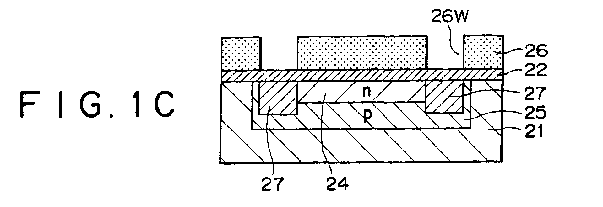
- the mask layer 23 is removed, and a third mask layer 26 having two openings 26w positioned over electrode forming areas at both ends of the semiconductor resistance region forming area is formed on the protective film 22.
- the mask layer 26 is formed by coating the protective layer 22 with a photoresist layer and forming the openings 26w in the photoresist layer by photolithography.
- Ions of an n-type impurity are implanted in the surface region of the substrate 21 through both the openings 26w of the mask layer 26 used as an ion implantation mask, to form two high concentration impurity doped regions 27.
- Si may be used as the n-type impurity, and in this case, an implantation energy may be set to 150 keV and a dose may be set to 3 ⁇ 10 13 cm -2 .
- both the photoresist layer 26 and the protective layer 22 on the substrate 21 are removed.
- the removal of the protective film 22 made from SiN may be performed by dipping the substrate 21 in a mixed acid (hydrofluoric acid and ammonia fluoride).
- the substrate 21 is then annealed, to activate the impurities doped in the regions 24, 25 and 27.
- a semiconductor resistance region 24R having a low impurity concentration and a sufficiently high sheet resistivity is formed from the region 24; two electrode extraction regions 27R each having a high impurity concentration are formed, at both ends of the semiconductor resistance region 24R, from the regions 27; and a p-type buried region 25B is formed, between the semiconductor resistance region 24R and the substrate region 21S, from the region 25.
- the annealing is performed in an As containing atmosphere, for example, an AsH 3 atmosphere, and the annealing temperature is set to be in a range of 800 to 850°C.
- an insulating layer 28 made from SiN is formed overall on the surface of the semi-insulating semiconductor substrate 21.
- the insulating layer 28 is formed by depositing SiN to a thickness of 300 nm by the plasma CVD process.
- a mask layer 29 having two openings 29w positioned over the electrode extraction regions 27R is formed on the insulating layer 28.
- the mask layer 29 is formed by coating the overall surface of the substrate 21 with a photoresist layer, and forming the openings 29W in the photoresist layer by photolithography.
- the insulating layer 28 is etched through the openings 29w of the mask layer 29 used as an etching mask by reactive ion etching using CF 4 as a reaction gas, to form openings 28w.
- an electrode metal layer 30 is formed overall on the mask layer 29 in such a manner as to be brought into contact with the electrode extraction regions 27 exposed to the outside through the openings 29w and 28w.
- the electrode metal layer 30 is formed by sequentially forming an AuGe layer having a thickness of 150 nm and an Ni layer having a thickness of 50 nm by a vapor-deposition process.
- the portion, on the photoresist layer 29, of the metal layer 30 is removed by a lift-off process, that is, by removing the photoresist layer 29, whereby the portions, on the electrode extraction regions 27R, of the metal layer 30 remain.
- the substrate 21 is then heated in a forming gas at about 450°C, to subject the electrode extraction regions 27R to an alloying treatment, whereby a pair of electrodes 30R are formed from the metal layer 30 being in ohmic contact with the electrode extraction regions 27R.
- a plurality of semiconductor resistance elements 12 can be simultaneously formed in a common compound semiconductor substrate 21, and further, other circuit elements may be also formed in the compound semiconductor substrate 21, to thus form a semiconductor integrated circuit device.
- the buried region 25B which has an impurity concentration higher than that of the substrate region 21S and lower than that of the semiconductor resistance region 24R, is formed between the semiconductor resistance region 24R and the substrate region 21S, it is possible to suppress the back gate effect due to a variation in effective concentration of an acceptor present in the substrate region and also suppress a variation in spread of a depletion layer toward the semiconductor resistance region, and hence to stabilize the characteristics of the semiconductor resistance region and also reduce the concentration in the semiconductor resistance region 24R and increase the resistance of the semiconductor resistance region 24R.
- the impurity doped regions 24 and 25 are formed by using the same mask 23
- the impurity doped regions 24 and 25, that is, the n-type semiconductor resistance region 24R and the p-type buried region 25B can be formed with a self-alignment positional relationship kept therebetween.
Abstract


Description
Claims (7)
- A semiconductor device having a semiconductor resistance element, comprising:a compound semiconductor substrate;an n-type semiconductor resistance region formed in the surface of said compound semiconductor substrate; anda p-type buried region provided between said n-type semiconductor resistance region and a substrate region formed by said compound semiconductor substrate.
- A semiconductor device having a semiconductor resistance element according to claim 1, wherein said compound semiconductor substrate is a semi-insulating substrate.
- A semiconductor device having a semiconductor resistance element according to claim 1, wherein an acceptor concentration in said p-type buried region is selected to be higher than an acceptor concentration in said substrate region and to be lower than a donor concentration in said n-type semiconductor resistance region.
- A semiconductor device having a semiconductor resistance element according to claim 1, wherein said p-type buried region is perfectly depleted.
- A semiconductor device having a semiconductor resistance element according to claim 1, wherein said n-type semiconductor resistance region and said p-type buried region are formed with a self-alignment positional relationship kept therebetween.
- A method of fabricating a semiconductor device having a semiconductor resistance element, comprising:a step of doping an n-type impurity in a selected region in the surface of a semi-insulating compound semiconductor substrate via a first mask layer formed on the surface of the compound semiconductor substrate, to form an n-type impurity doped region;a step of doping, after or before said step of forming the n-type impurity doped region, a p-type impurity in the surface of said compound semiconductor substrate via a second mask layer formed on the surface of said compound semiconductor substrate, to form a p-type impurity doped region;a step of heat-treating the compound semiconductor substrate, to activate the impurities in the n-type impurity doped region and the p-type impurity doped region, thereby forming an n-type semiconductor resistance region, and also forming a p-type buried region between the n-type semiconductor resistance region and a substrate region of the semiconductor substrate in such a manner as to bring the p-type buried region into contact with the n-type semiconductor resistance region; anda step of forming ohmic electrodes in the semiconductor resistance region.
- A method of fabricating a semiconductor device having a semiconductor resistance element according to claim 6, wherein the n-type impurity doped region and the p-type impurity doped region are formed in self-alignment by commonly using one mask layer as the first and second mask layers.
Applications Claiming Priority (2)
| Application Number | Priority Date | Filing Date | Title |
|---|---|---|---|
| JP2000153445A JP4599660B2 (en) | 2000-05-24 | 2000-05-24 | Semiconductor device having semiconductor resistance element and manufacturing method thereof |
| JP2000153445 | 2000-05-24 |
Publications (3)
| Publication Number | Publication Date |
|---|---|
| EP1158584A2 true EP1158584A2 (en) | 2001-11-28 |
| EP1158584A3 EP1158584A3 (en) | 2007-01-03 |
| EP1158584B1 EP1158584B1 (en) | 2012-09-26 |
Family
ID=18658699
Family Applications (1)
| Application Number | Title | Priority Date | Filing Date |
|---|---|---|---|
| EP01112470A Expired - Lifetime EP1158584B1 (en) | 2000-05-24 | 2001-05-22 | Fabrication method of a semiconductor device having semiconductor resistance element |
Country Status (3)
| Country | Link |
|---|---|
| US (2) | US6667538B2 (en) |
| EP (1) | EP1158584B1 (en) |
| JP (1) | JP4599660B2 (en) |
Cited By (1)
| Publication number | Priority date | Publication date | Assignee | Title |
|---|---|---|---|---|
| EP3193364A1 (en) * | 2016-01-18 | 2017-07-19 | Nexperia B.V. | Apparatus and associated method |
Families Citing this family (3)
| Publication number | Priority date | Publication date | Assignee | Title |
|---|---|---|---|---|
| JP3959032B2 (en) * | 2003-01-08 | 2007-08-15 | 松下電器産業株式会社 | Method for manufacturing solid-state imaging device |
| FR2884050B1 (en) * | 2005-04-01 | 2007-07-20 | St Microelectronics Sa | INTEGRATED CIRCUIT COMPRISING SUBSTRATE AND RESISTANCE |
| US7625819B2 (en) * | 2007-06-01 | 2009-12-01 | Macronix International Co., Ltd. | Interconnection process |
Citations (5)
| Publication number | Priority date | Publication date | Assignee | Title |
|---|---|---|---|---|
| US4228450A (en) * | 1977-10-25 | 1980-10-14 | International Business Machines Corporation | Buried high sheet resistance structure for high density integrated circuits with reach through contacts |
| JPS6260252A (en) * | 1985-09-09 | 1987-03-16 | Nec Corp | Semiconductor device |
| JPH04146665A (en) * | 1990-10-09 | 1992-05-20 | Sony Corp | Resistance element |
| JPH05315547A (en) * | 1992-05-13 | 1993-11-26 | Sumitomo Electric Ind Ltd | Resistance element and manufacture thereof |
| JPH1187621A (en) * | 1997-09-03 | 1999-03-30 | Mitsubishi Electric Corp | Injection resistor and method for forming the same |
Family Cites Families (11)
| Publication number | Priority date | Publication date | Assignee | Title |
|---|---|---|---|---|
| JPS53126875A (en) * | 1977-04-13 | 1978-11-06 | Hitachi Ltd | Gate protecting device |
| JPS5456777A (en) * | 1977-10-14 | 1979-05-08 | Nec Corp | Semiconductor device |
| FR2445617A1 (en) * | 1978-12-28 | 1980-07-25 | Ibm France | IMPROVED BREAKDOWN VOLTAGE RESISTANCE ACHIEVED BY DOUBLE ION IMPLANTATION IN A SEMICONDUCTOR SUBSTRATE AND MANUFACTURING METHOD THEREOF |
| JPS5718354A (en) * | 1980-07-09 | 1982-01-30 | Hitachi Ltd | Semiconductor integrated circuit |
| JPS612361A (en) * | 1984-06-15 | 1986-01-08 | Hitachi Micro Comput Eng Ltd | Electrostatic breakdown preventive element |
| JPS62143478A (en) * | 1985-12-18 | 1987-06-26 | Sanyo Electric Co Ltd | Junction-type field effect transistor |
| JPH01268049A (en) * | 1988-04-19 | 1989-10-25 | Sony Corp | Diffused resistor element |
| JPH03169063A (en) * | 1989-11-29 | 1991-07-22 | Nec Corp | Semiconductor integrated circuit device |
| JPH0467666A (en) * | 1990-07-09 | 1992-03-03 | Fujitsu Ltd | Semiconductor device |
| JPH05114699A (en) * | 1991-07-24 | 1993-05-07 | Fujitsu Ltd | Semiconductor resistor and method for setting its resistance value |
| JP4218073B2 (en) * | 1998-01-20 | 2009-02-04 | ソニー株式会社 | Semiconductor resistance element |
-
2000
- 2000-05-24 JP JP2000153445A patent/JP4599660B2/en not_active Expired - Fee Related
-
2001
- 2001-05-21 US US09/862,042 patent/US6667538B2/en not_active Expired - Fee Related
- 2001-05-22 EP EP01112470A patent/EP1158584B1/en not_active Expired - Lifetime
-
2003
- 2003-10-20 US US10/689,305 patent/US6902992B2/en not_active Expired - Fee Related
Patent Citations (5)
| Publication number | Priority date | Publication date | Assignee | Title |
|---|---|---|---|---|
| US4228450A (en) * | 1977-10-25 | 1980-10-14 | International Business Machines Corporation | Buried high sheet resistance structure for high density integrated circuits with reach through contacts |
| JPS6260252A (en) * | 1985-09-09 | 1987-03-16 | Nec Corp | Semiconductor device |
| JPH04146665A (en) * | 1990-10-09 | 1992-05-20 | Sony Corp | Resistance element |
| JPH05315547A (en) * | 1992-05-13 | 1993-11-26 | Sumitomo Electric Ind Ltd | Resistance element and manufacture thereof |
| JPH1187621A (en) * | 1997-09-03 | 1999-03-30 | Mitsubishi Electric Corp | Injection resistor and method for forming the same |
Cited By (4)
| Publication number | Priority date | Publication date | Assignee | Title |
|---|---|---|---|---|
| EP3193364A1 (en) * | 2016-01-18 | 2017-07-19 | Nexperia B.V. | Apparatus and associated method |
| CN106992168A (en) * | 2016-01-18 | 2017-07-28 | 安世有限公司 | Device and associated method |
| US10050101B2 (en) | 2016-01-18 | 2018-08-14 | Nexperia B.V. | Apparatus and associated method |
| CN106992168B (en) * | 2016-01-18 | 2022-05-24 | 安世有限公司 | Apparatus and associated methods |
Also Published As
| Publication number | Publication date |
|---|---|
| EP1158584B1 (en) | 2012-09-26 |
| US6667538B2 (en) | 2003-12-23 |
| JP2001332697A (en) | 2001-11-30 |
| US20040207045A1 (en) | 2004-10-21 |
| EP1158584A3 (en) | 2007-01-03 |
| US6902992B2 (en) | 2005-06-07 |
| US20020011630A1 (en) | 2002-01-31 |
| JP4599660B2 (en) | 2010-12-15 |
Similar Documents
| Publication | Publication Date | Title |
|---|---|---|
| US4546540A (en) | Self-aligned manufacture of FET | |
| US5036017A (en) | Method of making asymmetrical field effect transistor | |
| JPH03178135A (en) | Manufacture of insulating gate field effect transistor | |
| EP0305975B1 (en) | Compound semiconductor mesfet | |
| EP0145926B1 (en) | Polysilicon resistors compensated with double ion-implantation | |
| JPH03774B2 (en) | ||
| EP0461807B1 (en) | MESFET and manufacturing method therefor | |
| US4432008A (en) | Gold-doped IC resistor region | |
| EP0077737A2 (en) | Low capacitance field effect transistor | |
| US4523368A (en) | Semiconductor devices and manufacturing methods | |
| US6373108B1 (en) | Semiconductor device having reduced sheet resistance of source/drain regions | |
| US4804635A (en) | Method of manufacture of galluim arsenide field effect transistors | |
| US6902992B2 (en) | Method of fabricating semiconductor device having semiconductor resistance element | |
| USH291H (en) | Fully ion implanted junction field effect transistor | |
| US5972768A (en) | Method of manufacturing semiconductor device having low contact resistance | |
| US5159414A (en) | Junction field effect transistor of a compound semiconductor | |
| EP0338251B1 (en) | Method of manufacturing metal-semiconductor field effect transistors | |
| GB2074374A (en) | Method of making field effect transistors | |
| US6306763B1 (en) | Enhanced salicidation technique | |
| JPH0645598A (en) | Semiconductor device and manufacture thereof | |
| GB2140617A (en) | Methods of forming a field effect transistor | |
| JP2707436B2 (en) | Method for manufacturing field effect transistor | |
| JPH06204259A (en) | Manufacture of compound semiconductor device | |
| KR100243021B1 (en) | Method for manufacturing semiconductor device | |
| JPH02218164A (en) | Mis type field-effect transistor |
Legal Events
| Date | Code | Title | Description |
|---|---|---|---|
| PUAI | Public reference made under article 153(3) epc to a published international application that has entered the european phase |
Free format text: ORIGINAL CODE: 0009012 |
|
| AK | Designated contracting states |
Kind code of ref document: A2 Designated state(s): AT BE CH CY DE DK ES FI FR GB GR IE IT LI LU MC NL PT SE TR |
|
| AX | Request for extension of the european patent |
Free format text: AL;LT;LV;MK;RO;SI |
|
| PUAL | Search report despatched |
Free format text: ORIGINAL CODE: 0009013 |
|
| AK | Designated contracting states |
Kind code of ref document: A3 Designated state(s): AT BE CH CY DE DK ES FI FR GB GR IE IT LI LU MC NL PT SE TR |
|
| AX | Request for extension of the european patent |
Extension state: AL LT LV MK RO SI |
|
| 17P | Request for examination filed |
Effective date: 20070611 |
|
| AKX | Designation fees paid |
Designated state(s): DE FR GB |
|
| 17Q | First examination report despatched |
Effective date: 20070911 |
|
| REG | Reference to a national code |
Ref country code: DE Ref legal event code: R079 Ref document number: 60147152 Country of ref document: DE Free format text: PREVIOUS MAIN CLASS: H01L0029860500 Ipc: H01L0027080000 |
|
| GRAP | Despatch of communication of intention to grant a patent |
Free format text: ORIGINAL CODE: EPIDOSNIGR1 |
|
| RIC1 | Information provided on ipc code assigned before grant |
Ipc: H01L 27/08 20060101AFI20120312BHEP Ipc: H01L 29/8605 20060101ALI20120312BHEP |
|
| RTI1 | Title (correction) |
Free format text: FABRICATION METHOD OF A SEMICONDUCTOR DEVICE HAVING SEMICONDUCTOR RESISTANCE ELEMENT |
|
| GRAS | Grant fee paid |
Free format text: ORIGINAL CODE: EPIDOSNIGR3 |
|
| GRAA | (expected) grant |
Free format text: ORIGINAL CODE: 0009210 |
|
| RIN1 | Information on inventor provided before grant (corrected) |
Inventor name: IMOTO, TSUTOMU |
|
| AK | Designated contracting states |
Kind code of ref document: B1 Designated state(s): DE FR GB |
|
| RAP1 | Party data changed (applicant data changed or rights of an application transferred) |
Owner name: SONY CORPORATION |
|
| REG | Reference to a national code |
Ref country code: GB Ref legal event code: FG4D |
|
| REG | Reference to a national code |
Ref country code: DE Ref legal event code: R096 Ref document number: 60147152 Country of ref document: DE Effective date: 20121122 |
|
| PLBE | No opposition filed within time limit |
Free format text: ORIGINAL CODE: 0009261 |
|
| STAA | Information on the status of an ep patent application or granted ep patent |
Free format text: STATUS: NO OPPOSITION FILED WITHIN TIME LIMIT |
|
| 26N | No opposition filed |
Effective date: 20130627 |
|
| REG | Reference to a national code |
Ref country code: DE Ref legal event code: R097 Ref document number: 60147152 Country of ref document: DE Effective date: 20130627 |
|
| PGFP | Annual fee paid to national office [announced via postgrant information from national office to epo] |
Ref country code: GB Payment date: 20140521 Year of fee payment: 14 |
|
| PGFP | Annual fee paid to national office [announced via postgrant information from national office to epo] |
Ref country code: FR Payment date: 20140527 Year of fee payment: 14 Ref country code: DE Payment date: 20140521 Year of fee payment: 14 |
|
| REG | Reference to a national code |
Ref country code: DE Ref legal event code: R119 Ref document number: 60147152 Country of ref document: DE |
|
| GBPC | Gb: european patent ceased through non-payment of renewal fee |
Effective date: 20150522 |
|
| REG | Reference to a national code |
Ref country code: FR Ref legal event code: ST Effective date: 20160129 |
|
| PG25 | Lapsed in a contracting state [announced via postgrant information from national office to epo] |
Ref country code: DE Free format text: LAPSE BECAUSE OF NON-PAYMENT OF DUE FEES Effective date: 20151201 Ref country code: GB Free format text: LAPSE BECAUSE OF NON-PAYMENT OF DUE FEES Effective date: 20150522 |
|
| PG25 | Lapsed in a contracting state [announced via postgrant information from national office to epo] |
Ref country code: FR Free format text: LAPSE BECAUSE OF NON-PAYMENT OF DUE FEES Effective date: 20150601 |