USH291H - Fully ion implanted junction field effect transistor - Google Patents
Fully ion implanted junction field effect transistor Download PDFInfo
- Publication number
- USH291H USH291H US06/861,628 US86162886A USH291H US H291 H USH291 H US H291H US 86162886 A US86162886 A US 86162886A US H291 H USH291 H US H291H
- Authority
- US
- United States
- Prior art keywords
- source
- gate
- drain
- inp
- effect transistor
- Prior art date
- Legal status (The legal status is an assumption and is not a legal conclusion. Google has not performed a legal analysis and makes no representation as to the accuracy of the status listed.)
- Abandoned
Links
Images
Classifications
-
- H—ELECTRICITY
- H10—SEMICONDUCTOR DEVICES; ELECTRIC SOLID-STATE DEVICES NOT OTHERWISE PROVIDED FOR
- H10D—INORGANIC ELECTRIC SEMICONDUCTOR DEVICES
- H10D30/00—Field-effect transistors [FET]
- H10D30/01—Manufacture or treatment
- H10D30/051—Manufacture or treatment of FETs having PN junction gates
- H10D30/0512—Manufacture or treatment of FETs having PN junction gates of FETs having PN homojunction gates
-
- H—ELECTRICITY
- H10—SEMICONDUCTOR DEVICES; ELECTRIC SOLID-STATE DEVICES NOT OTHERWISE PROVIDED FOR
- H10D—INORGANIC ELECTRIC SEMICONDUCTOR DEVICES
- H10D30/00—Field-effect transistors [FET]
- H10D30/80—FETs having rectifying junction gate electrodes
- H10D30/83—FETs having PN junction gate electrodes
-
- H—ELECTRICITY
- H10—SEMICONDUCTOR DEVICES; ELECTRIC SOLID-STATE DEVICES NOT OTHERWISE PROVIDED FOR
- H10D—INORGANIC ELECTRIC SEMICONDUCTOR DEVICES
- H10D62/00—Semiconductor bodies, or regions thereof, of devices having potential barriers
- H10D62/10—Shapes, relative sizes or dispositions of the regions of the semiconductor bodies; Shapes of the semiconductor bodies
- H10D62/17—Semiconductor regions connected to electrodes not carrying current to be rectified, amplified or switched, e.g. channel regions
- H10D62/343—Gate regions of field-effect devices having PN junction gates
Definitions
- This invention pertains generally to field-effect transistors (FETs) and in particular to junction FETs made by ion implantation from III-V semiconductors.
- the velocity of the charge carriers and parastic elements play important roles in determining its high frequency performance.
- charge carrier velocity is proportional to the electric field with the proportionality constant being the drift mobility.
- the relationship becomes non linear.
- the drift velocity reaches a saturation value at fields above 5 ⁇ 10 4 V/cm.
- the drift velocity first reaches a peak and then declines to a saturation value. Since the low-field mobility of silicon is relatively small, the performance of GaAs and InP is expected to be superior to that of Si. InP is expected to operate at higher frequencies than GaAs due to its higher peak velocity.
- the higher reverse breakdown voltage and higher thermal conductivity of InP also gives it the potential for outperforming GaAs.
- MOSFET metal-semiconductor field-effect transistor
- a junction gate structure in InP circumvents the Schottky barrier problem and early work on diffused JFETs (surface diffusion using Zn dopants) have been reported.
- Ion implantation of the dopants is an attractive alternative approach since it is highly compatible with the fabrication of planar devices and monolithic circuits. Ion implantation has been used to make FETs from InP but these efforts have been limited to MESFETs. The inventor participated in research leading to the present invention that resulted in a doubly ion implanted InP JFET. However, this device needed to be isolated by an etch which created a mesa structure on which it was difficult to deposit interconnect lines.
- This invention is a method of making a planar JFET from III-V compounds and alloys in which both the n-region and p-regions are ion implanted in a semi-insulating substrate and in which the gate is further defined by selectively etching through the gate-implant region to the source/drain channel.
- InP was used as the substrate, 28 Si was implanted in the source and drain, and 9 Be was implanted in the gate region.
- Plasma etching defined a 1 micrometer gate.
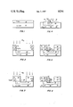
- FIG. 1 is a cross-sectional view of the substrate and undefined barrier layer from which the JFET is made.
- FIG. 2 is a cross-sectional view of the JFET following the first ion implantation.
- FIG. 3 is a cross-sectional view of the JFET following the second ion implantation.
- FIG. 4 is a cross-sectional view of the JFET following deposition of the gate metal.
- FIG. 5 is a cross-sectional view of the JFET following the deposition of the source/drain metal.
- FIG. 6 is a cross-sectional view of the JFET following the gate definition etch.
- JFETs Junction field-effect transistors
- InP InP
- III-V semiconductors III-V semiconductors
- double ion implantations which establish both the p-region and the n-region.
- the procedure is set forth in the context of a device made of InP the procedure is quite general and is not limited to InP.
- the example is limited to a discrete device it is readily understood that multiple devices can be fabricated on a single chip to form an integrated circuit.
- the JFET fabrication uses a substrate 10 of InP grown by the liquid encapsulated Czochralski method that is Fe-doped to be semi-insulating of resistivity greater than 10 7 ohm-cm.
- the surface of the InP substrate has a (100)-orientation.
- the substrate is first cleaned with organic solvents and etched in a 1:4 HIO 3 :H 2 O solution. Then a 500 nm thick barrier layer 12 of Si 3 N 4 is deposited on the (100) surface of the substrate 10.
- Alternative materials for the barrier 12 are SiO 2 or other etchable material.
- photoresist is deposited on the barrier layer 12 and photolithographically patterned to leave only photoresist portions 14 and 16 as illustrated in cross-sectional view in FIG. 2.
- the photoresist then acts as a mask when a plasma etching step removes all the exposed barrier layer but leaves the barrier layer portions 18 and 20.
- the wafer is ion implanted.
- the combination of photoresist portions 14 and 16 and barrier portions 18 and 20 serves as a mask so that only an initial active region 22 is implanted in an area 50 micrometers long and 300 micrometers wide.
- the initial ion implant is chosen to be 28 Si (isotopic silicon of atomic mass 28) so that the doping in the initial active region 22 is n-type.
- Two separate implant schedules are used: 9.4 ⁇ 10 12 cm -2 at 580 keV, 4.6 ⁇ 10 12 cm -2 at 280 keV and 7.0 ⁇ 10 12 cm -2 at 580 keV, 3.5 ⁇ 10 12 cm -2 at 280 keV.
- the first parameter is the surface density of the implanted ion and the second parameter is the energy of the ion.
- These implant schedules correspond to calculated atomic concentrations of 28 Si in the initial active region 22 of 2.5 ⁇ 10 17 cm -3 and 1.9 ⁇ 10 17 cm -3 respectively.
- the residual substrate 26 that was not implanted is left semi-insulating. The remaining photoresist portions 14 and 16 are then removed.
- a second step of creating a p type region from which a gate is formed new photoresist is applied in a pattern that defines a channel mask 28 and 30 as illustrated in cross section in FIG. 3.
- the aperture in the mask is 7 micrometers long.
- the wafer is then etched in a 1:4 HIO 3 :H 2 O for 30 sec to remove 50 nm of InP from the initial active region 22.
- This etching time is experimentally determined to yield the desired I DSS levels in the finished devices.
- the I DSS levels can be controlled by varying the parameters of the 9 Be implant of the implantation step to follow.
- the etching step further cleans the surface preparatory to the 9 Be implant and provides registration marks for later processing steps.
- the barrier portions 18 and 20 are left to serve as additional registration and to insure that the final p-implant overlays the n-implant over the entire width of the active region 34.
- the p-implant was accomplished by implanting 9 Be at a dose of 6 ⁇ 10 13 cm -2 at 30 keV resulting in an n-type extended gate region 32 extending part way into the active region 34.
- the thickness of the n-type active region 34 is thus reduced and the active region 34 can be considered to be divided into three parts, as shown in cross-sectional view in FIG. 4, a source end 36, a drain end 38, and a source/drain channel 40 connecting those ends.
- the photoresist 28 and 30 is removed by rinsing the wafer with acetone and the barrier portions 18 and 20 of Si 3 N 4 are stripped by immersion in HF.
- the chip When silicon or beryllium is implanted in InP, the chip needs to be annealed after the implant for two reasons. First the implantation produces structural damage to the crystalline InP which needs to be annealed out. Secondly in an annealing step the Be or Si diffuses to the desired lattice locations so that the implanted dopant will be activated.
- the Group V elements tend to dissociate from the surface thus producing a non-stoichiometric III-V semiconductor.
- Two techniques are commonly available to overcome the dissociation problem.
- the III-V material is coated with a layer of SiO 2 or Si 3 N 4 prior to the anneal.
- the second method called a capless anneal, requires annealing in an over pressure of PH 3 (phosphene) or AsH 3 .
- PH 3 phosphene
- AsH 3 phosphene
- the proximity anneal is accomplished by sandwiching the InP wafer between two silicon wafers coated on the InP side with Si 3 N 4 . The sandwich is then raised to the annealing temperature. The Group V phosphorus dissociates only to the extent that the small void between the InP and the Si 3 N 4 coating is saturated with phosphorus. The proximity anneal is performed at 700° C. for 15 minutes.
- the gate is defined by depositing by evaporation a gate metal first layer 42 and second layer 44. Note that these layers have not been drawn to scale in FIG. 4.
- the gate is placed as close as possible within processing limits to the source end 36 in order to minimize the source-gate resistance.
- the gate metal first layer 42 consists of AuZn in proportions of 95:5 wt % and is 50 nm thick.
- the gate metal second layer 44 consists of Au of 350 nm thickness.
- the first layer 42 and second layer 44 of the gate metal are then commonly defined by conventional photoresist lift-off techniques. Both layers 42 and 44 of the gate metal are 1 micrometers long by 300 micrometers wide in the direction transverse to the cross-section of FIG. 4.
- the source/drain contacts are defined by another photolithographic step as illustrated in cross-section in FIG. 5.
- First layer source and drain metals 46 and 48 are deposited of eutectic AuGe, i.e. in proportions of 88:12 wt % to a thickness of 100 nm.
- second layer source and drain metals 50 and 52 of Au are deposited to a thickness of 100 nm.
- a Cl 2 plasma etch which, as illustrated in FIG. 6, completely etches away the exposed p-type InP.
- the Cl 2 etch proceeds until the reverse gate source I-V characteristic shows low leakage current and a sharp breakdown.
- the etch leaves only a 1 micrometer long by 300 micrometer wide junction gate 54 overlaying the source/drain channel 40 of the active region 34.
- all the metal contacts are alloyed in a forming gas atmosphere at 400° C. for 45 sec.
- the effect of the elevated temperature is to drive the Ge from the first layer source/drain metals 46 and 48 into the active region 34 and the Zn from the first layer gate metal 42 into the Junction gate 54 thus forming ohmic contacts with the n type and p-type InP.
- Metallic interconnects can be deposited on a chip containing many of the devices described above so as to produce an integrated circuit.
- the JFET is essentially planar so there are no steep steps presenting coverage problems to an interconnect deposition.
- the only two etches in the final JFET which affect the planarity are the minor one between implants which can be replaced by a more systematic immplant and the gate etch which exposes the channel over which interconnects would not be placed. Neither etch creates a steep edge over which an interconnect would be deposited.
- the JFET can be improved by an additional implantation of 28 Si into the source end 36 and drain end 38 as illustrated in FIG. 4. A high dose will turn these ends 36 and 38 into n + thereby facilitating the making of ohmic contacts to each and more importantly reducing the source-drain resistance. The low resistance leads to higher frequency performance.
- the maximum mutual transconductance G m is measured to be 8 mS.
- the gate-source breakdown voltage is found to be 25 V.
- a doubly ion implanted JFET is not limited to InP.
- the same invention is expected to be particularly useful with InGaAs, an alloy of III-V materials useful for high speed electronics.
- InGaAs like InP, exhibits a low Schottky barrier which renders difficult the task of building InGaAs MESFETs.
- the alloys InGa 1-x As with x between 0.35 and 0.65 are expected to be useful for high speed devices.
- An alloy of the composition In 0 .53 Ga 0 .47 As is particularly useful because of both its speed and its lattice match to InP so that it can be easily grown epitaxially on InP.
- III-V alloy is the quatermary alloy.
- InGaAsP more accurately written as In 1-x Ga x As y P 1-y .
- This alloy can be lattice matched over a wide range of alloying.
- any of the alloys need to be made semi-insulating, either during growth or during subsequent processing.
Landscapes
- Junction Field-Effect Transistors (AREA)
Abstract
A method of making a planar junction field-effect transistor in which a semi-insulating substrate of a III-V semiconductor, particularly InP, is ion implanted by two ions to produce both an n-type region and a p-type region. The gate is further defined by selectively etching through the gate-implant region to the source/drain channel.
Description
This application is a continuation, of applicaiton Ser. No. 471,096, filed Mar. 1, 1983, now abandoned.
1. Field of the Invention
This invention pertains generally to field-effect transistors (FETs) and in particular to junction FETs made by ion implantation from III-V semiconductors.
2. Prior Art
Present-day semiconductor electronics is dominated by silicon technology. However, it is recognized that other semiconducting materials, though lacking silicon's technological maturity, offer the promise of improved speed and performance.
In a microwave FET, the velocity of the charge carriers and parastic elements play important roles in determining its high frequency performance. At low electric fields, charge carrier velocity is proportional to the electric field with the proportionality constant being the drift mobility. However, at higher electric fields the relationship becomes non linear. For Si, the drift velocity reaches a saturation value at fields above 5×10⁴ V/cm. For GaAs and InP, the drift velocity first reaches a peak and then declines to a saturation value. Since the low-field mobility of silicon is relatively small, the performance of GaAs and InP is expected to be superior to that of Si. InP is expected to operate at higher frequencies than GaAs due to its higher peak velocity. In addition, the higher reverse breakdown voltage and higher thermal conductivity of InP also gives it the potential for outperforming GaAs.
Early device designers, faced with the choice of GaAs, InP and other III-V compounds besides GaAs and InP, picked GaAs because of its perceived technological advantages. The primary FET structure for GaAs is the metal-semiconductor field-effect transistor (MESFET). MESFETs made from GaAs are relatively easy to fabricate because of the large Schottky barrier between the metal and the semiconductor. However, the Schottky barrier for InP and III-V alloys such as InGaAs is too small to easily fabricate Schottky barrier FETs. Thus InP and InGaAs were not extensively pursued for use in FETs.
A junction gate structure in InP circumvents the Schottky barrier problem and early work on diffused JFETs (surface diffusion using Zn dopants) have been reported. Ion implantation of the dopants is an attractive alternative approach since it is highly compatible with the fabrication of planar devices and monolithic circuits. Ion implantation has been used to make FETs from InP but these efforts have been limited to MESFETs. The inventor participated in research leading to the present invention that resulted in a doubly ion implanted InP JFET. However, this device needed to be isolated by an etch which created a mesa structure on which it was difficult to deposit interconnect lines.
Therefore it is an object of this invention to provide a high frequency field-effect transistor.
It is a further object of this invention to provide a junction field-effect transistor made of III-V semiconducting materials.
It is yet a further object of this invention to provide a simple method of making III-V junction field-effect transistors.
This invention is a method of making a planar JFET from III-V compounds and alloys in which both the n-region and p-regions are ion implanted in a semi-insulating substrate and in which the gate is further defined by selectively etching through the gate-implant region to the source/drain channel.
In one embodiment, InP was used as the substrate, 28 Si was implanted in the source and drain, and 9 Be was implanted in the gate region. Plasma etching defined a 1 micrometer gate.
FIG. 1 is a cross-sectional view of the substrate and undefined barrier layer from which the JFET is made.
FIG. 2 is a cross-sectional view of the JFET following the first ion implantation.
FIG. 3 is a cross-sectional view of the JFET following the second ion implantation.
FIG. 4 is a cross-sectional view of the JFET following deposition of the gate metal.
FIG. 5 is a cross-sectional view of the JFET following the deposition of the source/drain metal.
FIG. 6 is a cross-sectional view of the JFET following the gate definition etch.
Junction field-effect transistors (JFETs) can be easily fabricated in a planar geometry from InP and other III-V semiconductors by double ion implantations which establish both the p-region and the n-region. Although the procedure is set forth in the context of a device made of InP the procedure is quite general and is not limited to InP. In addition, although the example is limited to a discrete device it is readily understood that multiple devices can be fabricated on a single chip to form an integrated circuit.
Referring now to the drawings, wherein like reference numerals designate identical or corresponding parts throughout the several views, and more particularly to FIG. 1 thereof, the JFET fabrication uses a substrate 10 of InP grown by the liquid encapsulated Czochralski method that is Fe-doped to be semi-insulating of resistivity greater than 107 ohm-cm. The surface of the InP substrate has a (100)-orientation. In a first processing step of creating an n-type active region, the substrate is first cleaned with organic solvents and etched in a 1:4 HIO3 :H2 O solution. Then a 500 nm thick barrier layer 12 of Si3 N4 is deposited on the (100) surface of the substrate 10. Alternative materials for the barrier 12 are SiO2 or other etchable material.
Thereafter, photoresist is deposited on the barrier layer 12 and photolithographically patterned to leave only photoresist portions 14 and 16 as illustrated in cross-sectional view in FIG. 2. The photoresist then acts as a mask when a plasma etching step removes all the exposed barrier layer but leaves the barrier layer portions 18 and 20.
Then the wafer is ion implanted. The combination of photoresist portions 14 and 16 and barrier portions 18 and 20 serves as a mask so that only an initial active region 22 is implanted in an area 50 micrometers long and 300 micrometers wide. The initial ion implant is chosen to be 28 Si (isotopic silicon of atomic mass 28) so that the doping in the initial active region 22 is n-type. Two separate implant schedules are used: 9.4×1012 cm-2 at 580 keV, 4.6×1012 cm-2 at 280 keV and 7.0×1012 cm-2 at 580 keV, 3.5×1012 cm-2 at 280 keV. The first parameter is the surface density of the implanted ion and the second parameter is the energy of the ion. These implant schedules correspond to calculated atomic concentrations of 28 Si in the initial active region 22 of 2.5×1017 cm-3 and 1.9×1017 cm-3 respectively. The residual substrate 26 that was not implanted is left semi-insulating. The remaining photoresist portions 14 and 16 are then removed.
In a second step of creating a p type region from which a gate is formed, new photoresist is applied in a pattern that defines a channel mask 28 and 30 as illustrated in cross section in FIG. 3. The aperture in the mask is 7 micrometers long. The wafer is then etched in a 1:4 HIO3 :H2 O for 30 sec to remove 50 nm of InP from the initial active region 22. This etching time is experimentally determined to yield the desired IDSS levels in the finished devices. Alternatively the IDSS levels can be controlled by varying the parameters of the 9 Be implant of the implantation step to follow. The etching step further cleans the surface preparatory to the 9 Be implant and provides registration marks for later processing steps. The barrier portions 18 and 20 are left to serve as additional registration and to insure that the final p-implant overlays the n-implant over the entire width of the active region 34. The p-implant was accomplished by implanting 9 Be at a dose of 6×1013 cm-2 at 30 keV resulting in an n-type extended gate region 32 extending part way into the active region 34. The thickness of the n-type active region 34 is thus reduced and the active region 34 can be considered to be divided into three parts, as shown in cross-sectional view in FIG. 4, a source end 36, a drain end 38, and a source/drain channel 40 connecting those ends. Subsequent to the ion implantation the photoresist 28 and 30 is removed by rinsing the wafer with acetone and the barrier portions 18 and 20 of Si3 N4 are stripped by immersion in HF.
When silicon or beryllium is implanted in InP, the chip needs to be annealed after the implant for two reasons. First the implantation produces structural damage to the crystalline InP which needs to be annealed out. Secondly in an annealing step the Be or Si diffuses to the desired lattice locations so that the implanted dopant will be activated.
Unfortunately in a straight-forward anneal of III-V compounds with the surface exposed, the Group V elements tend to dissociate from the surface thus producing a non-stoichiometric III-V semiconductor. Two techniques are commonly available to overcome the dissociation problem. In the first method, the III-V material is coated with a layer of SiO2 or Si3 N4 prior to the anneal. However during the anneal cracking of the SiO2 or Si3 N4 due to thermal stress and possible Si out-diffusion can occur. The second method, called a capless anneal, requires annealing in an over pressure of PH3 (phosphene) or AsH3. Unfortunately both these gases are toxic and thus undesirable in a production environment.
Yet another method has been developed which avoids these problems in what is called a proximity or close-contact anneal. The proximity anneal is accomplished by sandwiching the InP wafer between two silicon wafers coated on the InP side with Si3 N4. The sandwich is then raised to the annealing temperature. The Group V phosphorus dissociates only to the extent that the small void between the InP and the Si3 N4 coating is saturated with phosphorus. The proximity anneal is performed at 700° C. for 15 minutes.
In a third step of placing contacts for the source, gate and drain, the gate is defined by depositing by evaporation a gate metal first layer 42 and second layer 44. Note that these layers have not been drawn to scale in FIG. 4. The gate is placed as close as possible within processing limits to the source end 36 in order to minimize the source-gate resistance. The gate metal first layer 42 consists of AuZn in proportions of 95:5 wt % and is 50 nm thick. The gate metal second layer 44 consists of Au of 350 nm thickness. The first layer 42 and second layer 44 of the gate metal are then commonly defined by conventional photoresist lift-off techniques. Both layers 42 and 44 of the gate metal are 1 micrometers long by 300 micrometers wide in the direction transverse to the cross-section of FIG. 4.
The source/drain contacts are defined by another photolithographic step as illustrated in cross-section in FIG. 5. First layer source and drain metals 46 and 48 are deposited of eutectic AuGe, i.e. in proportions of 88:12 wt % to a thickness of 100 nm. Then second layer source and drain metals 50 and 52 of Au are deposited to a thickness of 100 nm.
In a fourth step of solating the gate region, the structural definition is completed by a Cl2 plasma etch which, as illustrated in FIG. 6, completely etches away the exposed p-type InP. The Cl2 etch proceeds until the reverse gate source I-V characteristic shows low leakage current and a sharp breakdown. The etch leaves only a 1 micrometer long by 300 micrometer wide junction gate 54 overlaying the source/drain channel 40 of the active region 34.
In a fifth and final step, all the metal contacts are alloyed in a forming gas atmosphere at 400° C. for 45 sec. The effect of the elevated temperature is to drive the Ge from the first layer source/ drain metals 46 and 48 into the active region 34 and the Zn from the first layer gate metal 42 into the Junction gate 54 thus forming ohmic contacts with the n type and p-type InP.
Metallic interconnects can be deposited on a chip containing many of the devices described above so as to produce an integrated circuit. The JFET is essentially planar so there are no steep steps presenting coverage problems to an interconnect deposition. The only two etches in the final JFET which affect the planarity are the minor one between implants which can be replaced by a more systematic immplant and the gate etch which exposes the channel over which interconnects would not be placed. Neither etch creates a steep edge over which an interconnect would be deposited.
The JFET can be improved by an additional implantation of 28 Si into the source end 36 and drain end 38 as illustrated in FIG. 4. A high dose will turn these ends 36 and 38 into n+ thereby facilitating the making of ohmic contacts to each and more importantly reducing the source-drain resistance. The low resistance leads to higher frequency performance.
A InP JFET built according to the foregoing description with a gate length of 1 micrometer, a gate width of 300 micrometer, and a source-drain length of 7 micrometer had IDSS =100 mA, i.e. saturated drain current, for VG =0. The maximum mutual transconductance Gm is measured to be 8 mS. The gate-source breakdown voltage is found to be 25 V. The device when tested for RF response demonstrates a maximum available gain of 12 dB at 4 GHz, VDS =12 V and VG =2.1 V. At 6 GHz, VDS =9 V and VG =5 V, the maximum available gain is measured to be 5.5 dB. Improvements in performance are to be expected if the processing parameters were optimized. The optimizing procedure has not yet attempted.
Although a fabrication of an InP JFET has been described, it is to be appreciated that a doubly ion implanted JFET is not limited to InP. The same invention is expected to be particularly useful with InGaAs, an alloy of III-V materials useful for high speed electronics. InGaAs, like InP, exhibits a low Schottky barrier which renders difficult the task of building InGaAs MESFETs. The alloys InGa1-x As with x between 0.35 and 0.65 are expected to be useful for high speed devices. An alloy of the composition In0.53 Ga0.47 As is particularly useful because of both its speed and its lattice match to InP so that it can be easily grown epitaxially on InP. Yet another favorable III-V alloy is the quatermary alloy. InGaAsP, more accurately written as In1-x Gax Asy P1-y. This alloy can be lattice matched over a wide range of alloying. For this invention any of the alloys need to be made semi-insulating, either during growth or during subsequent processing.
Obviously, additional modifications and variations of the present invention are possible in light of the above teachings. It is therefore to be understood that within the scope of the appended claims, the invention may be practiced otherwise than as specifically described herein.
Claims (1)
1. A field-effect transistor, comprising:
a residual substrate essentially consisting of semi-insulating InP;
an active region essentially consisting of n-type InP doped with Si, the source end and drain end of which have a surface substantially co-planar with the surface of the residual substrate and which are connected by a source/drain channel part of said active region the upper surface of which is recessed below the surface of said source end and said drain end;
a gate consisting of p-type InP doped with Be oerlaying a portion of said source/drain channel but not the entire source/drain channel and contacting said source/drain channel on only one side,
a gate contact comprising Au-Zn overlaying said gate;
a drain contact comprising eutectic AuGe overlaying said drain end; and
a source contact comprising eutectic AuGe overlaying said source end.
Priority Applications (1)
| Application Number | Priority Date | Filing Date | Title |
|---|---|---|---|
| US06/861,628 USH291H (en) | 1983-03-01 | 1986-05-07 | Fully ion implanted junction field effect transistor |
Applications Claiming Priority (2)
| Application Number | Priority Date | Filing Date | Title |
|---|---|---|---|
| US47109683A | 1983-03-01 | 1983-03-01 | |
| US06/861,628 USH291H (en) | 1983-03-01 | 1986-05-07 | Fully ion implanted junction field effect transistor |
Related Parent Applications (1)
| Application Number | Title | Priority Date | Filing Date |
|---|---|---|---|
| US47109683A Continuation | 1983-03-01 | 1983-03-01 |
Publications (1)
| Publication Number | Publication Date |
|---|---|
| USH291H true USH291H (en) | 1987-06-02 |
Family
ID=27043325
Family Applications (1)
| Application Number | Title | Priority Date | Filing Date |
|---|---|---|---|
| US06/861,628 Abandoned USH291H (en) | 1983-03-01 | 1986-05-07 | Fully ion implanted junction field effect transistor |
Country Status (1)
| Country | Link |
|---|---|
| US (1) | USH291H (en) |
Cited By (7)
| Publication number | Priority date | Publication date | Assignee | Title |
|---|---|---|---|---|
| US5051376A (en) * | 1987-01-26 | 1991-09-24 | Mitsubishi Monsanto Chemical Co, Ltd. | Method for producing semiconductor device and semiconductor device produced thereby |
| US5068705A (en) * | 1990-07-31 | 1991-11-26 | Texas Instruments Incorporated | Junction field effect transistor with bipolar device and method |
| US5182233A (en) * | 1989-08-02 | 1993-01-26 | Kabushiki Kaisha Toshiba | Compound semiconductor pellet, and method for dicing compound semiconductor wafer |
| US5196358A (en) * | 1989-12-29 | 1993-03-23 | The United States Of America As Represented By The Secretary Of The Navy | Method of manufacturing InP junction FETS and junction HEMTS using dual implantation and double nitride layers |
| US5409569A (en) * | 1992-09-30 | 1995-04-25 | Alps Electric Co., Ltd. | Etchant, detergent and device/apparatus manufacturing method |
| US6211539B1 (en) * | 1983-10-21 | 2001-04-03 | Lucent Technologies Inc. | Semi-insulated indium phosphide based compositions |
| US20140353751A1 (en) * | 2013-05-30 | 2014-12-04 | International Business Machines Corporation | Local interconnects by metal-iii-v alloy wiring in semi-insulating iii-v substrates |
Citations (14)
| Publication number | Priority date | Publication date | Assignee | Title |
|---|---|---|---|---|
| GB1290419A (en) | 1970-12-23 | 1972-09-27 | ||
| US3725136A (en) | 1971-06-01 | 1973-04-03 | Texas Instruments Inc | Junction field effect transistor and method of fabrication |
| US3914784A (en) | 1973-12-10 | 1975-10-21 | Hughes Aircraft Co | Ion Implanted gallium arsenide semiconductor devices fabricated in semi-insulating gallium arsenide substrates |
| US3967305A (en) | 1969-03-27 | 1976-06-29 | Mcdonnell Douglas Corporation | Multichannel junction field-effect transistor and process |
| US4145233A (en) | 1978-05-26 | 1979-03-20 | Ncr Corporation | Method for making narrow channel FET by masking and ion-implantation |
| US4163984A (en) | 1978-01-27 | 1979-08-07 | Raytheon Company | Field effect transistor |
| US4185291A (en) | 1977-06-30 | 1980-01-22 | Matsushita Electric Industrial Co., Ltd. | Junction-type field effect transistor and method of making the same |
| US4285763A (en) | 1980-01-29 | 1981-08-25 | Bell Telephone Laboratories, Incorporated | Reactive ion etching of III-V semiconductor compounds |
| US4310570A (en) | 1979-12-20 | 1982-01-12 | Eaton Corporation | Field-effect transistors with micron and submicron gate lengths |
| US4321613A (en) | 1978-05-31 | 1982-03-23 | The Secretary Of State For Defence In Her Britannic Majesty's Government Of The United Kingdom Of Great Britain And Northern Ireland | Field effect devices and their fabrication |
| US4327475A (en) | 1979-11-26 | 1982-05-04 | Nippon Telegraph & Telephone Public Corporation | Method of manufacturing a FET device disposed in a compound s/c layer on a semi-insulating substrate |
| US4452646A (en) | 1981-09-28 | 1984-06-05 | Mcdonnell Douglas Corporation | Method of making planar III-V compound device by ion implantation |
| US4468851A (en) | 1981-12-14 | 1984-09-04 | The United States Of America As Represented By The Secretary Of The Navy | Process for making a heterojunction source-drain insulated gate field-effect transistors utilizing diffusion to form the lattice |
| US4471367A (en) | 1981-12-04 | 1984-09-11 | At&T Bell Laboratories | MESFET Using a shallow junction gate structure on GaInAs |
-
1986
- 1986-05-07 US US06/861,628 patent/USH291H/en not_active Abandoned
Patent Citations (14)
| Publication number | Priority date | Publication date | Assignee | Title |
|---|---|---|---|---|
| US3967305A (en) | 1969-03-27 | 1976-06-29 | Mcdonnell Douglas Corporation | Multichannel junction field-effect transistor and process |
| GB1290419A (en) | 1970-12-23 | 1972-09-27 | ||
| US3725136A (en) | 1971-06-01 | 1973-04-03 | Texas Instruments Inc | Junction field effect transistor and method of fabrication |
| US3914784A (en) | 1973-12-10 | 1975-10-21 | Hughes Aircraft Co | Ion Implanted gallium arsenide semiconductor devices fabricated in semi-insulating gallium arsenide substrates |
| US4185291A (en) | 1977-06-30 | 1980-01-22 | Matsushita Electric Industrial Co., Ltd. | Junction-type field effect transistor and method of making the same |
| US4163984A (en) | 1978-01-27 | 1979-08-07 | Raytheon Company | Field effect transistor |
| US4145233A (en) | 1978-05-26 | 1979-03-20 | Ncr Corporation | Method for making narrow channel FET by masking and ion-implantation |
| US4321613A (en) | 1978-05-31 | 1982-03-23 | The Secretary Of State For Defence In Her Britannic Majesty's Government Of The United Kingdom Of Great Britain And Northern Ireland | Field effect devices and their fabrication |
| US4327475A (en) | 1979-11-26 | 1982-05-04 | Nippon Telegraph & Telephone Public Corporation | Method of manufacturing a FET device disposed in a compound s/c layer on a semi-insulating substrate |
| US4310570A (en) | 1979-12-20 | 1982-01-12 | Eaton Corporation | Field-effect transistors with micron and submicron gate lengths |
| US4285763A (en) | 1980-01-29 | 1981-08-25 | Bell Telephone Laboratories, Incorporated | Reactive ion etching of III-V semiconductor compounds |
| US4452646A (en) | 1981-09-28 | 1984-06-05 | Mcdonnell Douglas Corporation | Method of making planar III-V compound device by ion implantation |
| US4471367A (en) | 1981-12-04 | 1984-09-11 | At&T Bell Laboratories | MESFET Using a shallow junction gate structure on GaInAs |
| US4468851A (en) | 1981-12-14 | 1984-09-04 | The United States Of America As Represented By The Secretary Of The Navy | Process for making a heterojunction source-drain insulated gate field-effect transistors utilizing diffusion to form the lattice |
Non-Patent Citations (4)
| Title |
|---|
| Applied Physics Letters, vol. 34, Feb. 1979 by Armiento, pp. 229-231. |
| J. B. Boos et al., Fully Implanted InP Junction FET's, IEEE Electron Deviceetters, vol. EDL-3, pp. 256-258, 1982. |
| K. J. Sleger et al., Low Noise Ion Implanted InP FET's IEEE Transactions of Electron Devices, vol. ED-28, pp. 1031-1034, 1981. |
| R. Yeats et al., Research on InGaAs FETs., Final Report on Contract N00014-78-C-0380 AD-A108016, 1981. |
Cited By (8)
| Publication number | Priority date | Publication date | Assignee | Title |
|---|---|---|---|---|
| US6211539B1 (en) * | 1983-10-21 | 2001-04-03 | Lucent Technologies Inc. | Semi-insulated indium phosphide based compositions |
| US5051376A (en) * | 1987-01-26 | 1991-09-24 | Mitsubishi Monsanto Chemical Co, Ltd. | Method for producing semiconductor device and semiconductor device produced thereby |
| US5182233A (en) * | 1989-08-02 | 1993-01-26 | Kabushiki Kaisha Toshiba | Compound semiconductor pellet, and method for dicing compound semiconductor wafer |
| US5196358A (en) * | 1989-12-29 | 1993-03-23 | The United States Of America As Represented By The Secretary Of The Navy | Method of manufacturing InP junction FETS and junction HEMTS using dual implantation and double nitride layers |
| US5068705A (en) * | 1990-07-31 | 1991-11-26 | Texas Instruments Incorporated | Junction field effect transistor with bipolar device and method |
| US5409569A (en) * | 1992-09-30 | 1995-04-25 | Alps Electric Co., Ltd. | Etchant, detergent and device/apparatus manufacturing method |
| US20140353751A1 (en) * | 2013-05-30 | 2014-12-04 | International Business Machines Corporation | Local interconnects by metal-iii-v alloy wiring in semi-insulating iii-v substrates |
| US8941123B2 (en) * | 2013-05-30 | 2015-01-27 | International Business Machines Corporation | Local interconnects by metal-III-V alloy wiring in semi-insulating III-V substrates |
Similar Documents
| Publication | Publication Date | Title |
|---|---|---|
| US4377030A (en) | Metallization of selectively implanted AIII -BV compound semiconductors | |
| EP0725432B1 (en) | Refractory gate heterostructure field effect transistor and method | |
| DE10024510A1 (en) | Heterojunction-type field effect transistor for portable telephone, has gate electrode formed over p-type low resistance area of barrier layer inbetween source and drain electrodes | |
| US5350709A (en) | Method of doping a group III-V compound semiconductor | |
| EP0338251B1 (en) | Method of manufacturing metal-semiconductor field effect transistors | |
| EP0194197B1 (en) | Heterojunction bipolar transistor and process for fabricating same | |
| US5610410A (en) | III-V compound semiconductor device with Schottky electrode of increased barrier height | |
| EP0201873B1 (en) | A method of the production of a metal semiconductor field effect transistor and said transistor | |
| EP0080714B1 (en) | Hetero-junction semiconductor device | |
| US3866310A (en) | Method for making the self-aligned gate contact of a semiconductor device | |
| KR100329251B1 (en) | Semiconductor device and manufacturing method thereof | |
| JPH0259624B2 (en) | ||
| USH291H (en) | Fully ion implanted junction field effect transistor | |
| US5101245A (en) | Field effect transistor and method for making same | |
| EP0165433A2 (en) | High-speed field-effect transistor | |
| US4701422A (en) | Method of adjusting threshold voltage subsequent to fabrication of transistor | |
| US5159414A (en) | Junction field effect transistor of a compound semiconductor | |
| KR100563884B1 (en) | Manufacturing method of a junction field effect transistor | |
| US5541424A (en) | Permeable base transistor having laminated layers | |
| WO1982001619A1 (en) | Method of making a planar iii-v bipolar transistor by selective ion implantation and a device made therewith | |
| US6902992B2 (en) | Method of fabricating semiconductor device having semiconductor resistance element | |
| US5242846A (en) | Method of manufacturing a junction field effect transistor | |
| EP0124277B1 (en) | Field effect transistor for integrated circuits | |
| KR910006751B1 (en) | Semiconductor integrated circuit device and its manufacturing method | |
| DE69028644T2 (en) | Integrated circuit and manufacturing process |
Legal Events
| Date | Code | Title | Description |
|---|---|---|---|
| STPP | Information on status: patent application and granting procedure in general |
Free format text: DEFENSIVE PUBLICATION OR SIR FILE |