EP0077737A2 - Low capacitance field effect transistor - Google Patents
Low capacitance field effect transistor Download PDFInfo
- Publication number
- EP0077737A2 EP0077737A2 EP82401916A EP82401916A EP0077737A2 EP 0077737 A2 EP0077737 A2 EP 0077737A2 EP 82401916 A EP82401916 A EP 82401916A EP 82401916 A EP82401916 A EP 82401916A EP 0077737 A2 EP0077737 A2 EP 0077737A2
- Authority
- EP
- European Patent Office
- Prior art keywords
- layer
- substrate
- semiconductor material
- regions
- insulating material
- Prior art date
- Legal status (The legal status is an assumption and is not a legal conclusion. Google has not performed a legal analysis and makes no representation as to the accuracy of the status listed.)
- Withdrawn
Links
- 230000005669 field effect Effects 0.000 title abstract description 9
- 239000004065 semiconductor Substances 0.000 claims abstract description 42
- 239000000758 substrate Substances 0.000 claims abstract description 42
- 239000011810 insulating material Substances 0.000 claims abstract description 27
- 229910021420 polycrystalline silicon Inorganic materials 0.000 claims abstract description 22
- 239000012535 impurity Substances 0.000 claims abstract description 19
- 229910052710 silicon Inorganic materials 0.000 claims abstract description 14
- 239000010703 silicon Substances 0.000 claims abstract description 14
- 239000011521 glass Substances 0.000 claims abstract description 12
- 238000004519 manufacturing process Methods 0.000 claims abstract description 9
- 238000000034 method Methods 0.000 claims description 35
- 239000000463 material Substances 0.000 claims description 30
- 238000000151 deposition Methods 0.000 claims description 9
- 229910052715 tantalum Inorganic materials 0.000 claims description 8
- GUVRBAGPIYLISA-UHFFFAOYSA-N tantalum atom Chemical compound [Ta] GUVRBAGPIYLISA-UHFFFAOYSA-N 0.000 claims description 8
- DLYUQMMRRRQYAE-UHFFFAOYSA-N tetraphosphorus decaoxide Chemical compound O1P(O2)(=O)OP3(=O)OP1(=O)OP2(=O)O3 DLYUQMMRRRQYAE-UHFFFAOYSA-N 0.000 claims description 7
- 239000004020 conductor Substances 0.000 claims description 5
- 239000002019 doping agent Substances 0.000 claims description 3
- 230000001590 oxidative effect Effects 0.000 claims 3
- 241000237519 Bivalvia Species 0.000 claims 1
- 235000020639 clam Nutrition 0.000 claims 1
- VYPSYNLAJGMNEJ-UHFFFAOYSA-N Silicium dioxide Chemical compound O=[Si]=O VYPSYNLAJGMNEJ-UHFFFAOYSA-N 0.000 abstract description 36
- 235000012239 silicon dioxide Nutrition 0.000 abstract description 18
- 239000000377 silicon dioxide Substances 0.000 abstract description 18
- XUIMIQQOPSSXEZ-UHFFFAOYSA-N Silicon Chemical compound [Si] XUIMIQQOPSSXEZ-UHFFFAOYSA-N 0.000 abstract description 12
- BHEPBYXIRTUNPN-UHFFFAOYSA-N hydridophosphorus(.) (triplet) Chemical compound [PH] BHEPBYXIRTUNPN-UHFFFAOYSA-N 0.000 abstract description 9
- 229910021421 monocrystalline silicon Inorganic materials 0.000 abstract description 3
- XUIMIQQOPSSXEZ-NJFSPNSNSA-N silicon-30 atom Chemical compound [30Si] XUIMIQQOPSSXEZ-NJFSPNSNSA-N 0.000 abstract description 2
- 239000010410 layer Substances 0.000 abstract 3
- 230000008021 deposition Effects 0.000 abstract 1
- 239000002356 single layer Substances 0.000 abstract 1
- 125000004429 atom Chemical group 0.000 description 4
- 230000006870 function Effects 0.000 description 4
- QVGXLLKOCUKJST-UHFFFAOYSA-N atomic oxygen Chemical compound [O] QVGXLLKOCUKJST-UHFFFAOYSA-N 0.000 description 3
- 230000015572 biosynthetic process Effects 0.000 description 3
- 238000005229 chemical vapour deposition Methods 0.000 description 3
- 238000009792 diffusion process Methods 0.000 description 3
- 238000010438 heat treatment Methods 0.000 description 3
- 229910052760 oxygen Inorganic materials 0.000 description 3
- 239000001301 oxygen Substances 0.000 description 3
- ZOXJGFHDIHLPTG-UHFFFAOYSA-N Boron Chemical compound [B] ZOXJGFHDIHLPTG-UHFFFAOYSA-N 0.000 description 2
- XYFCBTPGUUZFHI-UHFFFAOYSA-N Phosphine Chemical compound P XYFCBTPGUUZFHI-UHFFFAOYSA-N 0.000 description 2
- 238000003491 array Methods 0.000 description 2
- 229910052796 boron Inorganic materials 0.000 description 2
- 238000005530 etching Methods 0.000 description 2
- 238000005468 ion implantation Methods 0.000 description 2
- 230000000873 masking effect Effects 0.000 description 2
- 230000003647 oxidation Effects 0.000 description 2
- 238000007254 oxidation reaction Methods 0.000 description 2
- 238000001020 plasma etching Methods 0.000 description 2
- VZGDMQKNWNREIO-UHFFFAOYSA-N tetrachloromethane Chemical compound ClC(Cl)(Cl)Cl VZGDMQKNWNREIO-UHFFFAOYSA-N 0.000 description 2
- TXEYQDLBPFQVAA-UHFFFAOYSA-N tetrafluoromethane Chemical compound FC(F)(F)F TXEYQDLBPFQVAA-UHFFFAOYSA-N 0.000 description 2
- 229910052785 arsenic Inorganic materials 0.000 description 1
- RQNWIZPPADIBDY-UHFFFAOYSA-N arsenic atom Chemical compound [As] RQNWIZPPADIBDY-UHFFFAOYSA-N 0.000 description 1
- 238000003486 chemical etching Methods 0.000 description 1
- 230000000593 degrading effect Effects 0.000 description 1
- 230000000694 effects Effects 0.000 description 1
- 238000009413 insulation Methods 0.000 description 1
- 229910052751 metal Inorganic materials 0.000 description 1
- 239000002184 metal Substances 0.000 description 1
- 238000012986 modification Methods 0.000 description 1
- 230000004048 modification Effects 0.000 description 1
- 229910052757 nitrogen Inorganic materials 0.000 description 1
- 125000004437 phosphorous atom Chemical group 0.000 description 1
- -1 phosphorous ions Chemical class 0.000 description 1
- 229910052698 phosphorus Inorganic materials 0.000 description 1
- 229910000073 phosphorus hydride Inorganic materials 0.000 description 1
- 238000011112 process operation Methods 0.000 description 1
- 238000004544 sputter deposition Methods 0.000 description 1
- 239000000126 substance Substances 0.000 description 1
Images

Classifications
-
- H—ELECTRICITY
- H01—ELECTRIC ELEMENTS
- H01L—SEMICONDUCTOR DEVICES NOT COVERED BY CLASS H10
- H01L29/00—Semiconductor devices specially adapted for rectifying, amplifying, oscillating or switching and having potential barriers; Capacitors or resistors having potential barriers, e.g. a PN-junction depletion layer or carrier concentration layer; Details of semiconductor bodies or of electrodes thereof ; Multistep manufacturing processes therefor
- H01L29/66—Types of semiconductor device ; Multistep manufacturing processes therefor
- H01L29/66007—Multistep manufacturing processes
- H01L29/66075—Multistep manufacturing processes of devices having semiconductor bodies comprising group 14 or group 13/15 materials
- H01L29/66227—Multistep manufacturing processes of devices having semiconductor bodies comprising group 14 or group 13/15 materials the devices being controllable only by the electric current supplied or the electric potential applied, to an electrode which does not carry the current to be rectified, amplified or switched, e.g. three-terminal devices
- H01L29/66409—Unipolar field-effect transistors
- H01L29/66477—Unipolar field-effect transistors with an insulated gate, i.e. MISFET
- H01L29/66568—Lateral single gate silicon transistors
- H01L29/66651—Lateral single gate silicon transistors with a single crystalline channel formed on the silicon substrate after insulating device isolation
-
- H—ELECTRICITY
- H01—ELECTRIC ELEMENTS
- H01L—SEMICONDUCTOR DEVICES NOT COVERED BY CLASS H10
- H01L21/00—Processes or apparatus adapted for the manufacture or treatment of semiconductor or solid state devices or of parts thereof
- H01L21/02—Manufacture or treatment of semiconductor devices or of parts thereof
- H01L21/02104—Forming layers
- H01L21/02107—Forming insulating materials on a substrate
- H01L21/02225—Forming insulating materials on a substrate characterised by the process for the formation of the insulating layer
- H01L21/02227—Forming insulating materials on a substrate characterised by the process for the formation of the insulating layer formation by a process other than a deposition process
- H01L21/0223—Forming insulating materials on a substrate characterised by the process for the formation of the insulating layer formation by a process other than a deposition process formation by oxidation, e.g. oxidation of the substrate
- H01L21/02233—Forming insulating materials on a substrate characterised by the process for the formation of the insulating layer formation by a process other than a deposition process formation by oxidation, e.g. oxidation of the substrate of the semiconductor substrate or a semiconductor layer
- H01L21/02236—Forming insulating materials on a substrate characterised by the process for the formation of the insulating layer formation by a process other than a deposition process formation by oxidation, e.g. oxidation of the substrate of the semiconductor substrate or a semiconductor layer group IV semiconductor
- H01L21/02238—Forming insulating materials on a substrate characterised by the process for the formation of the insulating layer formation by a process other than a deposition process formation by oxidation, e.g. oxidation of the substrate of the semiconductor substrate or a semiconductor layer group IV semiconductor silicon in uncombined form, i.e. pure silicon
-
- H—ELECTRICITY
- H01—ELECTRIC ELEMENTS
- H01L—SEMICONDUCTOR DEVICES NOT COVERED BY CLASS H10
- H01L21/00—Processes or apparatus adapted for the manufacture or treatment of semiconductor or solid state devices or of parts thereof
- H01L21/02—Manufacture or treatment of semiconductor devices or of parts thereof
- H01L21/02104—Forming layers
- H01L21/02107—Forming insulating materials on a substrate
- H01L21/02225—Forming insulating materials on a substrate characterised by the process for the formation of the insulating layer
- H01L21/02227—Forming insulating materials on a substrate characterised by the process for the formation of the insulating layer formation by a process other than a deposition process
- H01L21/02255—Forming insulating materials on a substrate characterised by the process for the formation of the insulating layer formation by a process other than a deposition process formation by thermal treatment
-
- H—ELECTRICITY
- H01—ELECTRIC ELEMENTS
- H01L—SEMICONDUCTOR DEVICES NOT COVERED BY CLASS H10
- H01L21/00—Processes or apparatus adapted for the manufacture or treatment of semiconductor or solid state devices or of parts thereof
- H01L21/02—Manufacture or treatment of semiconductor devices or of parts thereof
- H01L21/02104—Forming layers
- H01L21/02107—Forming insulating materials on a substrate
- H01L21/02296—Forming insulating materials on a substrate characterised by the treatment performed before or after the formation of the layer
- H01L21/02299—Forming insulating materials on a substrate characterised by the treatment performed before or after the formation of the layer pre-treatment
-
- H—ELECTRICITY
- H01—ELECTRIC ELEMENTS
- H01L—SEMICONDUCTOR DEVICES NOT COVERED BY CLASS H10
- H01L21/00—Processes or apparatus adapted for the manufacture or treatment of semiconductor or solid state devices or of parts thereof
- H01L21/02—Manufacture or treatment of semiconductor devices or of parts thereof
- H01L21/02104—Forming layers
- H01L21/02365—Forming inorganic semiconducting materials on a substrate
- H01L21/02367—Substrates
- H01L21/0237—Materials
- H01L21/02373—Group 14 semiconducting materials
- H01L21/02381—Silicon, silicon germanium, germanium
-
- H—ELECTRICITY
- H01—ELECTRIC ELEMENTS
- H01L—SEMICONDUCTOR DEVICES NOT COVERED BY CLASS H10
- H01L21/00—Processes or apparatus adapted for the manufacture or treatment of semiconductor or solid state devices or of parts thereof
- H01L21/02—Manufacture or treatment of semiconductor devices or of parts thereof
- H01L21/02104—Forming layers
- H01L21/02365—Forming inorganic semiconducting materials on a substrate
- H01L21/02518—Deposited layers
- H01L21/02521—Materials
- H01L21/02524—Group 14 semiconducting materials
- H01L21/02532—Silicon, silicon germanium, germanium
-
- H—ELECTRICITY
- H01—ELECTRIC ELEMENTS
- H01L—SEMICONDUCTOR DEVICES NOT COVERED BY CLASS H10
- H01L21/00—Processes or apparatus adapted for the manufacture or treatment of semiconductor or solid state devices or of parts thereof
- H01L21/02—Manufacture or treatment of semiconductor devices or of parts thereof
- H01L21/02104—Forming layers
- H01L21/02365—Forming inorganic semiconducting materials on a substrate
- H01L21/02612—Formation types
- H01L21/02617—Deposition types
- H01L21/02636—Selective deposition, e.g. simultaneous growth of mono- and non-monocrystalline semiconductor materials
- H01L21/02639—Preparation of substrate for selective deposition
-
- H—ELECTRICITY
- H01—ELECTRIC ELEMENTS
- H01L—SEMICONDUCTOR DEVICES NOT COVERED BY CLASS H10
- H01L29/00—Semiconductor devices specially adapted for rectifying, amplifying, oscillating or switching and having potential barriers; Capacitors or resistors having potential barriers, e.g. a PN-junction depletion layer or carrier concentration layer; Details of semiconductor bodies or of electrodes thereof ; Multistep manufacturing processes therefor
- H01L29/02—Semiconductor bodies ; Multistep manufacturing processes therefor
- H01L29/04—Semiconductor bodies ; Multistep manufacturing processes therefor characterised by their crystalline structure, e.g. polycrystalline, cubic or particular orientation of crystalline planes
-
- H—ELECTRICITY
- H01—ELECTRIC ELEMENTS
- H01L—SEMICONDUCTOR DEVICES NOT COVERED BY CLASS H10
- H01L29/00—Semiconductor devices specially adapted for rectifying, amplifying, oscillating or switching and having potential barriers; Capacitors or resistors having potential barriers, e.g. a PN-junction depletion layer or carrier concentration layer; Details of semiconductor bodies or of electrodes thereof ; Multistep manufacturing processes therefor
- H01L29/02—Semiconductor bodies ; Multistep manufacturing processes therefor
- H01L29/06—Semiconductor bodies ; Multistep manufacturing processes therefor characterised by their shape; characterised by the shapes, relative sizes, or dispositions of the semiconductor regions ; characterised by the concentration or distribution of impurities within semiconductor regions
- H01L29/0603—Semiconductor bodies ; Multistep manufacturing processes therefor characterised by their shape; characterised by the shapes, relative sizes, or dispositions of the semiconductor regions ; characterised by the concentration or distribution of impurities within semiconductor regions characterised by particular constructional design considerations, e.g. for preventing surface leakage, for controlling electric field concentration or for internal isolations regions
- H01L29/0642—Isolation within the component, i.e. internal isolation
- H01L29/0649—Dielectric regions, e.g. SiO2 regions, air gaps
- H01L29/0653—Dielectric regions, e.g. SiO2 regions, air gaps adjoining the input or output region of a field-effect device, e.g. the source or drain region
Definitions
- This invention relates to integrated circuits, and in particular, to a compact field effect transistor structure having very low capacitance and a method for fabricating it.
- FET field effect transistor
- spaced apart source and drain regions are formed in an underlying semiconductor substrate.
- gate oxide is formed on top of the gate oxide.
- a gate electrode fabricated from an electrically conductive material, is deposited and defined.
- the gate electrode will typically be fabricated from metal or doped polycrystalline silicon.
- a channel may be implanted or otherwise fabricated between the source and drain regions.
- Such prior art FET's suffer from a number of disadvantages.
- Typically such structures have high capacitance between the source and substrate and between the drain and substrate, herein referred to as source/drain to substrate capacitance.
- source/drain to substrate capacitance In addition, such structures have low punch through voltage between the source and drain.
- the source/drain to substrate capacitance may be reduced by lowering the impurity concentration of the substrate, lowering the impurity concentration also tends to reduce the punch through voltage.
- both parameters deteriorate rapidly as the length of an enhancement mode FET channel is reduced below 1 micron because the depletion width of the source and drain regions are of about the same magnitude.
- a general object of this invention is to provide an improved field effect transistor and a method of making same.
- a transistor structure fabricated according to the invention comprises a semiconductor substrate, first and second spaced apart regions of insulating material disposed on the substrate and separated from each other by an intervening region of the substrate, a layer of semiconductor material disposed across the first and the second regions and across the intervening region of the semiconductor substrate, a layer of insulating material disposed across the surface of the layer of semiconductor material, and an electrode overlying at least that portion of the layer of insulating material which overlies the intervening semiconductor substrate.
- a method of fabricating an integrated circuit transistor structure comprises forming a first layer of insulating material over first and second spaced apart regions of a semiconductor substrate, the first and second regions being separated by an intervening region of the semiconductor substrate, depositing a layer of selected conductivity type semiconductor material over the layer of insulating material and the intervening region, introducing opposite conductivity type impurity into the layer of semiconductor material overlying the layer of insulating material, forming a second layer of insulating material over the layer of semiconductor material, and fabricating an electrically conductive region over at least that portion of the second layer of insulating material overlying the intervening region.
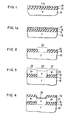
- the integrated circuit structure depicted in Figure 1 may be fabricated using known techniques. As shown in Figure 1 on a suitable P conductivity semiconductor substrate 10, for example, doped with 5 x 10 16 atoms per cubic centimeter of boron, a layer of silicon dioxide 12 is formed, In the preferred embodi ment silicon dioxide layer 12 is approximately 3,000 Angstroms thick and is fabricated by using any well known technique, for example, thermal oxidation. One such technique is to heat substrate 10 in an oxygen atmosphere to a temperature of 1000°C for 90 minutes. After fabrication of silicon dioxide 12, a relatively thin layer of phosphorous pentoxide (P 2 0 5 ) glass 15 is formed on the upper surface of silicon dioxide 12.
- P 2 0 5 phosphorous pentoxide
- the phosphorous glass 15 is 100 Angstroms thick and is fabricated by chemical vapor deposition.
- phosphine and oxygen are passed over the wafer to create the layer of phosphorous pentoxide on its surface.
- the underlying silicon dioxide 12 will dissolve slightly allowing the upper approximately 1000 Angstroms of layer 12 to become doped with phosphorous ions.
- the resulting structure may then be further processed as described in conjunction with Figures 2 through 7.
- FIG. la An alternative structure which may be utilized as a starting point for the process described in conjunction with Figures 2 through 7 is the structure shown in Figure la.
- substrate 10 and silicon dioxide layer 12 are fabricated in the same manner as discussed in conjunction with Figure 1.
- a layer of tantalum 16 approximately 500 Angstroms thick. Tantalum layer 16 may be fabricated by sputtering in a vacuum or by other known processes.
- a relatively thin layer of polycrystalline silicon 17 is deposited, for example, by chemical vapor deposition. The polycrystalline silicon 17 is then heavily doped with N conductivity type impurities.
- the doping concentra- t ion of layer 17 is 10 20 phosphorous atoms per cubic centimeter. This may be achieved by well known diffusion or ion implantation techniques.
- Another technique for forming the tantalum/polycrystalline silicon layers is to use chemical vapor deposition to deposit tantalum 16, deposit polycrystalline silicon 17, and dope silicon layer 17 all in one operation.
- FIG. 2 The structure from either Figure 1 or Figure la is then subjected to further integrated circuit processing operations as described in Figure 2 and subsequent.
- Figures 2-7 illustrate the subsequent process operations in which the structure of Figure 1 is used.
- an opening 20 is made through phosphorous glass 15 and silicon dioxide 12. Opening 20 may be created using known photolithographic integrated circuit fabrication techniques, for example, forming a first mask and etching by chemicals or plasma. According to ene such technique, layers 12 and 15 are removed by plasma etching with carbon tetrafluoride. If the structure shown in Figure la is utilized, then a first mask is formed and the opening through layer 17 is made with carbon tetrachloride plasma. Layers 16 and 12 are then etched using carbon tetrafluoride plasma.
- a layer of epitaxial silicon 21 is deposited across the upper surface of the structure shown in Figure 2.
- the epitaxial silicon 21 is deposited approximately 5,000 Angstroms thick using a low pressure process to prevent the dopant in layer 15 from diffusing into what will become the channel 24 of the transistor structure.
- region 24 where the epitaxial silicon 21 contacts the upper surface of substrate 10 monocrystalline silicon will be formed.
- Region 24 of layer 21 is then doped to an appropriate level, for example, by ion implantation to a concentration of 5 x 10 atoms per cubic centimeter of boron.
- the combined structure shown in Figure 3 is then heated to cause the phosphorous from the phosphorous glass 15 to diffuse out into epitaxial layer 21 in regions 27 and 28. In the preferred embodiment this is achieved by heating the structure to a 900°C for 40 minutes.
- the resulting N resistivity will be 10 ohms per square. Impurity concentrations between 5 x 10 19 and 10 20 atoms per cubic centimeter have been found suitable for the fabrication of regions 27 and 28 in the structure depicted. Because region 24 of epitaxial layer 21 does not overlie phosphorous glass 15, no source of N conductivity type impurities is present for diffusion into region 24. Moreover, because the N conductivity type impurity diffuses in polycrystalline silicon 21 approximately four times faster than in monocrystalline silicon 24, the effective width of region 24 will be only slightly reduced by any lateral diffusion which occurs.
- N doped regions 27 and 28 may be then defined using a second mask and well-known photolithographic techniques. Outside these boundaries epitaxial layer 21 will be removed using well known chemical etching, plasma etching, or other techniques.
- a layer of silicon dioxide 25 is next formed on the upper surface of epitaxial layer 21.
- layer 25 is fabricated by heating the underlying structure in an oxygen atmosphere to a temperature of about 800°C for 4 hours to form about 300 Angstroms of silicon dioxide on the upper surface of the P conductivity type portion of epitaxial layer 21 and about 1000 Angstroms of silicon dioxide on the upper surface of the N conductivity type portions of layer 21.
- the different rate of formation of silicon dioxide on underlying N and P conductivity type doped regions is a known phenomenon which is discussed in further detail in C. P. Ho et al. "Thermal Oxidation of Heavily Doped Silicon", J. Electrochem. Soc. 125, 665 (1978).
- a layer of polycrystalline silicon 30 is then formed across the upper surface of silicon dioxide 25.
- Layer 30 may be deposited as N conductivity type doped polycrystalline silicon or may be deposited as relatively pure polycrystalline silicon which is subsequently doped with an appropriate impurity, for example, arsenic or phosphorous.
- the impurity concentration of layer 30 is approximately 10 20 atoms per cubic centimeter of phosphorous.
- Undesired portions of layer 30 may then be removed using well known photolithographic and etching techniques to define a gate electrode as shown in Figure 5.
- the result of the process described is a field effect transistor of the enhancement mode type.
- the source/drain regions, gate oxide, and the oxide surrounding the gate oxide are all self-aligned.
- the tantalum lines 17 beneath the source/drain regions will function as very low resistance electrical connections to the source/drain regions.
- This embodiment is particularly advantageous when the field effect transistor depicted is to be utilized in a semiconductor memory.
- the tantalum lines 17 will function as bit or word lines, while other subsequently formed lines will function as word or bit lines, respectively.
- the transistor structure of Figures 5-7 is particularly advantageous as a field effect transistor because it may be fabricated using relatively few masking steps and has exceptionally low capacitance between the source/drain and the substrate.
- the low capacitance results from the layer of silicon dioxide 12 separating the source/drain regions from the substrate 10.
- the structure shown is completely self-aligned, that is, once the gate region 20 is defined, the source/drain regions and thicker oxide surrounding the gate are "automatically” fabricated on each side of the gate region without masking tolerances.
- Figure 6 is a top view of the structure shown in Figure 5.
- the boundaries have been displaced slightly to display the extent of the depicted regions.
- the coincident edges of the source/drain and channel have been displaced slightly to illustrate the boundaries of these regions.
- Gate electrode 30 completely overlies channel 24, which separates the source and drain. Because the channel will usually be wider than any contact to the source and drain, the source and drain may be reduced in width away from the channel as shown.
- Figure 7 shows a cross-sectional view of the structure shown in Figures 5 and 6, illustrating the manner in which the gate electrode 30 overlies the channel 24.
- the gate oxide separates the gate 30 from channel 24, while oxide 12 and glass 15 separate gate 30 from the substrate 10 as shown.
Landscapes
- Engineering & Computer Science (AREA)
- Microelectronics & Electronic Packaging (AREA)
- Power Engineering (AREA)
- General Physics & Mathematics (AREA)
- Computer Hardware Design (AREA)
- Physics & Mathematics (AREA)
- Condensed Matter Physics & Semiconductors (AREA)
- Manufacturing & Machinery (AREA)
- Chemical & Material Sciences (AREA)
- Ceramic Engineering (AREA)
- Crystallography & Structural Chemistry (AREA)
- Materials Engineering (AREA)
- Thin Film Transistor (AREA)
Abstract
A compact field effect transistor having extremely low source/drain to substrate capacitance is disclosed, together with a method of fabricating it. The source 27 and drain 25 regions of the FET are fabricated on an underlying layer of insulating material 12, typically silicon dioxide, while the gate region including a channel 24, is fabricated directly on the semiconductor substrate 10. The source/drain 27/25 and gate 24 regions are all simultaneously formed by deposition of a single layer of epitaxial silicon 21. In this manner a monocrystalline silicon gate region 24 is created with polycrystalline silicon source/drain regions 27/25. The different rate of growth of silicon dioxide over monocrystalline 24 and polycrystalline silicon 27/25 is utilized to create the gate oxide, while an overlying layer of doped polycrystalline silicon 30 serves as the gate electrode. The source/drain regions are typically doped by an impurity diffused from a layer of phosphorous glass deposited between the insulating material and the source/drain regions.
Description
- This invention relates to integrated circuits, and in particular, to a compact field effect transistor structure having very low capacitance and a method for fabricating it.
- Many different types of field effect transistor (FET) structures and processes for fabricating them are now known. In conventional FET's of the prior art, spaced apart source and drain regions are formed in an underlying semiconductor substrate. A relatively thin layer of silicon dioxide, commonly termed gate oxide, is formed on the surface of the substrate between the source and drain regions. On top of the gate oxide a gate electrode, fabricated from an electrically conductive material, is deposited and defined. The gate electrode will typically be fabricated from metal or doped polycrystalline silicon. In enhancement mode field effect transistors a channel may be implanted or otherwise fabricated between the source and drain regions.
- Unfortunately, such prior art FET's suffer from a number of disadvantages. Typically such structures have high capacitance between the source and substrate and between the drain and substrate, herein referred to as source/drain to substrate capacitance. In addition, such structures have low punch through voltage between the source and drain. Although the source/drain to substrate capacitance may be reduced by lowering the impurity concentration of the substrate, lowering the impurity concentration also tends to reduce the punch through voltage. Furthermore, both parameters deteriorate rapidly as the length of an enhancement mode FET channel is reduced below 1 micron because the depletion width of the source and drain regions are of about the same magnitude.
- The processes by which prior art FFT structures are formed also result in undesired consequences. For example, in conventional silicon gate FET fabrication processes a polycrystalline silicon gate electrode is deposited and defined. The gate electrode itself then functions as a mask for the introduction of impurities to define the source and drain regions. Because these regions tend to diffuse under the edge of the gate, undesired gate/source and gate/drain capacitances are created through the thin gate oxide. These capacitances have increasingly undesirable effects as increasingly larger memory arrays are fabricated.
- Furthermore, prior art arrays of silicon gate FET's are difficult to fabricate with uniformly thin layers of insulation beneath the gate electrode. This is in part due to lifting of the edges of the polycrystalline silicon gate as surrounding regions of the silicon substrate are oxidized. The lifting of the gate causes the turn-on potential of individual transistors within an array to vary from one to another, thereby degrading performance of the array.
- A general object of this invention is to provide an improved field effect transistor and a method of making same.
- In one embodiment a transistor structure fabricated according to the invention comprises a semiconductor substrate, first and second spaced apart regions of insulating material disposed on the substrate and separated from each other by an intervening region of the substrate, a layer of semiconductor material disposed across the first and the second regions and across the intervening region of the semiconductor substrate, a layer of insulating material disposed across the surface of the layer of semiconductor material, and an electrode overlying at least that portion of the layer of insulating material which overlies the intervening semiconductor substrate.
- In one embodiment a method of fabricating an integrated circuit transistor structure according to the invention comprises forming a first layer of insulating material over first and second spaced apart regions of a semiconductor substrate, the first and second regions being separated by an intervening region of the semiconductor substrate, depositing a layer of selected conductivity type semiconductor material over the layer of insulating material and the intervening region, introducing opposite conductivity type impurity into the layer of semiconductor material overlying the layer of insulating material, forming a second layer of insulating material over the layer of semiconductor material, and fabricating an electrically conductive region over at least that portion of the second layer of insulating material overlying the intervening region.
-
- Figure 1 is a cross-sectional view of an integrated circuit structure which may be fabricated using known techniques and which is a starting point for the process of this invention.
- Figure la illustrates an alternative cross-section which may also be utilized in fabricating the transistor structure of this invention.
- Figure 2 is a subsequent cross-sectional view of the structure shown in Figure 1 after definition of the gate region.
- Figure 3 is a subsequent cross-sectional view of the structure shown in Figure 2 after depositing epitaxial silicon and doping that silicon.
- Figure 4 is a subsequent cross-sectional view illustrating the appearance of the structure after formation of the gate oxide.
- Figure 5 is a subsequent cross-sectional view after formation of the gate electrode..
- Figure 6 is a top view of the structure shown in Figure 5.
- Figure 7 is a cross-sectional view of the structure shown in Figure 6 taken perpendicular to the cross-section shown in Figure 6.
- The integrated circuit structure depicted in Figure 1 may be fabricated using known techniques. As shown in Figure 1 on a suitable P
conductivity semiconductor substrate 10, for example, doped with 5 x 10¹⁶ atoms per cubic centimeter of boron, a layer ofsilicon dioxide 12 is formed, In the preferred embodi mentsilicon dioxide layer 12 is approximately 3,000 Angstroms thick and is fabricated by using any well known technique, for example, thermal oxidation. One such technique is to heatsubstrate 10 in an oxygen atmosphere to a temperature of 1000°C for 90 minutes. After fabrication ofsilicon dioxide 12, a relatively thin layer of phosphorous pentoxide (P205)glass 15 is formed on the upper surface ofsilicon dioxide 12. In the preferred embodiment thephosphorous glass 15 is 100 Angstroms thick and is fabricated by chemical vapor deposition. In such a process phosphine and oxygen are passed over the wafer to create the layer of phosphorous pentoxide on its surface. During subsequent heating, for example, for 30 minutes at 1000°C, theunderlying silicon dioxide 12 will dissolve slightly allowing the upper approximately 1000 Angstroms oflayer 12 to become doped with phosphorous ions. The resulting structure may then be further processed as described in conjunction with Figures 2 through 7. - An alternative structure which may be utilized as a starting point for the process described in conjunction with Figures 2 through 7 is the structure shown in Figure la. As shown in Figure la,
substrate 10 andsilicon dioxide layer 12 are fabricated in the same manner as discussed in conjunction with Figure 1. On the upper surface ofsilicon dioxide 12, however, is formed a layer of tantalum 16 approximately 500 Angstroms thick. Tantalum layer 16 may be fabricated by sputtering in a vacuum or by other known processes. On the upper surface of tantalum 16 a relatively thin layer ofpolycrystalline silicon 17, on the order of 1000 Angstroms thick, is deposited, for example, by chemical vapor deposition. Thepolycrystalline silicon 17 is then heavily doped with N conductivity type impurities. For example, in the preferred embodiment the doping concentra- tion oflayer 17 is 1020 phosphorous atoms per cubic centimeter. This may be achieved by well known diffusion or ion implantation techniques. Another technique for forming the tantalum/polycrystalline silicon layers is to use chemical vapor deposition to deposit tantalum 16, depositpolycrystalline silicon 17, and dopesilicon layer 17 all in one operation. - The structure from either Figure 1 or Figure la is then subjected to further integrated circuit processing operations as described in Figure 2 and subsequent. Figures 2-7 illustrate the subsequent process operations in which the structure of Figure 1 is used. As shown in Figure 2, an
opening 20 is made throughphosphorous glass 15 andsilicon dioxide 12.Opening 20 may be created using known photolithographic integrated circuit fabrication techniques, for example, forming a first mask and etching by chemicals or plasma. According to ene such technique,layers layer 17 is made with carbon tetrachloride plasma.Layers 16 and 12 are then etched using carbon tetrafluoride plasma. - As next shown in Figure 3, a layer of
epitaxial silicon 21 is deposited across the upper surface of the structure shown in Figure 2. In the preferred embodiment theepitaxial silicon 21 is deposited approximately 5,000 Angstroms thick using a low pressure process to prevent the dopant inlayer 15 from diffusing into what will become thechannel 24 of the transistor structure. Inregion 24 where theepitaxial silicon 21 contacts the upper surface ofsubstrate 10, monocrystalline silicon will be formed. Inregions epitaxial silicon 21 overliesphosphorous glass 15, polycrystalline silicon will be formed.Region 24 oflayer 21 is then doped to an appropriate level, for example, by ion implantation to a concentration of 5 x 10 atoms per cubic centimeter of boron. - The combined structure shown in Figure 3 is then heated to cause the phosphorous from the
phosphorous glass 15 to diffuse out intoepitaxial layer 21 inregions regions region 24 ofepitaxial layer 21 does not overliephosphorous glass 15, no source of N conductivity type impurities is present for diffusion intoregion 24. Moreover, because the N conductivity type impurity diffuses inpolycrystalline silicon 21 approximately four times faster than inmonocrystalline silicon 24, the effective width ofregion 24 will be only slightly reduced by any lateral diffusion which occurs. - The outer lateral boundaries (shown in Figure 6) of N doped
regions epitaxial layer 21 will be removed using well known chemical etching, plasma etching, or other techniques. - As shown in Figure 4, a layer of
silicon dioxide 25 is next formed on the upper surface ofepitaxial layer 21. In thepreferred embodiment layer 25 is fabricated by heating the underlying structure in an oxygen atmosphere to a temperature of about 800°C for 4 hours to form about 300 Angstroms of silicon dioxide on the upper surface of the P conductivity type portion ofepitaxial layer 21 and about 1000 Angstroms of silicon dioxide on the upper surface of the N conductivity type portions oflayer 21. The different rate of formation of silicon dioxide on underlying N and P conductivity type doped regions is a known phenomenon which is discussed in further detail in C. P. Ho et al. "Thermal Oxidation of Heavily Doped Silicon", J. Electrochem. Soc. 125, 665 (1978). - A layer of
polycrystalline silicon 30 is then formed across the upper surface ofsilicon dioxide 25.Layer 30 may be deposited as N conductivity type doped polycrystalline silicon or may be deposited as relatively pure polycrystalline silicon which is subsequently doped with an appropriate impurity, for example, arsenic or phosphorous. In the preferred embodiment the impurity concentration oflayer 30 is approximately 1020 atoms per cubic centimeter of phosphorous. Undesired portions oflayer 30 may then be removed using well known photolithographic and etching techniques to define a gate electrode as shown in Figure 5. - As shown in Figures 5-7 the result of the process described is a field effect transistor of the enhancement mode type. The source/drain regions, gate oxide, and the oxide surrounding the gate oxide are all self-aligned. The process eliminates lifting of the gate electrode. Electrical connections to the source/drain regions may be made by suitable openings in
silicon dioxide layer 25 at locations not shown in Figures 5-7. - In an alternative embodiment in which the structure of Figure la is utilized as a starting structure, the
tantalum lines 17 beneath the source/drain regions will function as very low resistance electrical connections to the source/drain regions. This embodiment is particularly advantageous when the field effect transistor depicted is to be utilized in a semiconductor memory. In such an application thetantalum lines 17 will function as bit or word lines, while other subsequently formed lines will function as word or bit lines, respectively. - The transistor structure of Figures 5-7 is particularly advantageous as a field effect transistor because it may be fabricated using relatively few masking steps and has exceptionally low capacitance between the source/drain and the substrate. The low capacitance results from the layer of
silicon dioxide 12 separating the source/drain regions from thesubstrate 10. In addition, the structure shown is completely self-aligned, that is, once thegate region 20 is defined, the source/drain regions and thicker oxide surrounding the gate are "automatically" fabricated on each side of the gate region without masking tolerances. - Figure 6 is a top view of the structure shown in Figure 5. For clarity, where boundaries of regions are fabricated aligned, the boundaries have been displaced slightly to display the extent of the depicted regions. For example, the coincident edges of the source/drain and channel have been displaced slightly to illustrate the boundaries of these regions.
Gate electrode 30 completely overlieschannel 24, which separates the source and drain. Because the channel will usually be wider than any contact to the source and drain, the source and drain may be reduced in width away from the channel as shown. - Figure 7 shows a cross-sectional view of the structure shown in Figures 5 and 6, illustrating the manner in which the
gate electrode 30 overlies thechannel 24. The gate oxide separates thegate 30 fromchannel 24, whileoxide 12 andglass 15separate gate 30 from thesubstrate 10 as shown. - Although two embodiments of the process and structure of this invention-have been described above, it will be apparent to those skilled in the art that numerous variations and modifications may be made without departing from the scope of the invention as set forth in the appended claims. For example, the conductivity types of the various regions may be changed.
Claims (30)
1. A method of fabricating an integrated circuit transistor structure characterized by:
forming a first layer of insulating material over first and second spaced apart regions of a semiconductor substrate, the first and the second regions being separated by an intervening region of the substrate;
depositing a layer of semiconductor material over the layer of insulating material and the intervening region;
introducing a first conductivity type impurity into that portion of the layer of semiconductor material overlying the intervening region and introducing an opposite conductivity type impurity into that portion of the layer of semiconductor material overlying the layer of insulating material;
forming a second layer of insulating material over the layer of semiconductor material; and
fabricating an electrically conductive region over at least that portion of the second layer of insulating material overlying the intervening region.
2. The method of claim 1 characterized by the step of fabricating a third layer of insulating material over the first and second spaced apart regions prior to the step of depositing a layer of selected conductivity type semiconductor material.
3. The method of claim 2 characterized in that the third layer of insulating material comprises a source of opposite conductivity type impurity.
4. The method of claim 2 or 3 characterized in that the third layer of insulating material comprises P2O5.
5. The method of any previous claim characterized in that the step of forming a first layer of insulating material comprises oxidizing the semiconductor substrate.
6. The method of any previous claim characterized in that the step of forming a second layer of insulating material comprises oxidizing the layer of semiconductor material.
7. The method of claim 6 characterized in that the layer of semiconductor material oxidizes more rapidly over the first and second spaced apart regions than over the intervening region of the substrate.
8. The method of any one of claims 2-7 characterized in that the step of fabricating an electrically conductive region comprises:
depositing a layer of polycrystalline silicon;
introducing impurities into the layer of polycrystalline silicon; and
removing undesired regions of the layer of polycrystalline silicon.
9. The method of any previous claim characterized in that a step of depositing an electrically conductive layer on the first layer of insulating material is performed following the step of forming a first layer of insulating material.
10. The method of claim 9 characterized in that a step of depositing a layer of polycrystalline silicon follows the step of depositing an electrically conductive layer.
11. A method of fabricating an integrated circuit transistor structure characterized by:
forming first and second spaced apart regions of oxidized semiconductor material overlaid by at least one selected layer on a semiconductor substrate;
depositing a layer of semiconductor material over the substrate and the at least one selected layer to thereby create regions of polycrystalline semiconductor material over the at least one selected layer and a region of monocrystalline semiconductor material over the substrate;
oxidizing the layer of semiconductor material; and forming an electrically conductive region of material over at least that portion of the oxidized layer of semiconductor material formed on the monocrystalline semiconductor material.
12. The method of claim 11 characterized in that the at least one selected layer comprises a first layer as a source of impurity dopant.
13. The method of claim 12 characterized in that the first layer provides impurity dopants for the overlying layer of semiconductor material.
14. The method of claim 13 characterized in that that at least one layer includes a second layer comprising electrically conductive material beneath the first layer.
15. An integrated circuit transistor structure characterized by:
a semiconductor substrate;
first and second spaced apart regions of insulating material disposed on the substrate, the first and second regions being separated by an intervening region of the substrate;
a layer of semiconductor material disposed across the first and the second regions and across the intervening region of the substrate;
a layer of insulating material disposed across the surface of the layer of semiconductor material; and
an electrode overlying at least that portion of the layer of insulating material which overlies the intervening region of the substrate.
16. The structure of claim 15 characterized in that the first and the second regions each comprise an oxide of the substrate.
17. The structure of claim 15 or 16 characterized in that the layer of insulating material comprises an oxide of the substrate.
18. The structure of claim 15, 16 or 17 characterized in that the substrate comprises silicon.
19. The structure of any one of clams 15-18 characterized in that the electrode comprises electrically conductive polycrystalline silicon.
20. The structure of any one of claims 15-19 characterized in that the layer of insulating material is thicker over the first and the second spaced apart regions than over the intervening region of the substrate.
21. The structure of claim 20 characterized in that the electrode comprises N conductivity type doped polycrystalline silicon.
22. The structure of any one of claims 15-21 characterized in that glass is formed over the first and the second spaced apart regions and beneath the layer of semiconductor material.
23. The structure of claim 22 or 23 characterized in that the layer of glass comprises a source of impurity.
24. The structure of claim 22 or 23 characterized in that the glass comprises P2O5.
25. The structure of any one of claims 15-25 characterized in that a layer of electrically conductive material is deposited between the first spaced apart region and the layer of semiconductor material, and between the second spaced apart region and the layer of semiconductor material.
26. The structure of claim 25 characterized in that a layer of polycrystalline silicon is disposed over the layer of electrically conductive material.
27. The structure of claim 25 or 26 characterized in that the electrically conductive material comprises tantalum.
28. The structure of any one of claims 23-27 characterized in that the layer of glass comprises a source of impurity for doping selected regions of the layer of semiconductor material.
29. The structure of claim 28 characterized in that the selected regions of the layer of semiconductor material do not include that portion of the layer of semiconductor material disposed across the intervening region of the substrate.
30. The structure of any one of claims 22-29 characterized in that said layer of semiconductor material comprises silicon which is monocrystalline where disposed on the substrate and polycrystalline where disposed on the at least one layer;
Applications Claiming Priority (2)
| Application Number | Priority Date | Filing Date | Title |
|---|---|---|---|
| US31300381A | 1981-10-19 | 1981-10-19 | |
| US313003 | 1981-10-19 |
Publications (2)
| Publication Number | Publication Date |
|---|---|
| EP0077737A2 true EP0077737A2 (en) | 1983-04-27 |
| EP0077737A3 EP0077737A3 (en) | 1984-11-07 |
Family
ID=23213956
Family Applications (1)
| Application Number | Title | Priority Date | Filing Date |
|---|---|---|---|
| EP82401916A Withdrawn EP0077737A3 (en) | 1981-10-19 | 1982-10-19 | Low capacitance field effect transistor |
Country Status (2)
| Country | Link |
|---|---|
| EP (1) | EP0077737A3 (en) |
| JP (1) | JPS5878466A (en) |
Cited By (11)
| Publication number | Priority date | Publication date | Assignee | Title |
|---|---|---|---|---|
| DE3408535A1 (en) * | 1983-05-30 | 1984-12-06 | Mitsubishi Denki K.K., Tokio/Tokyo | Semiconductor device of the MOS type and production process for it |
| WO1987004563A1 (en) * | 1986-01-25 | 1987-07-30 | Plessey Overseas Limited | Methods for fabricating transistors and mos transistors fabricated by such methods |
| EP0119400B1 (en) * | 1983-02-17 | 1987-08-05 | Nissan Motor Co., Ltd. | A vertical-type mosfet and method of fabricating the same |
| NL8700279A (en) * | 1986-02-07 | 1987-09-01 | Nippon Telegraph & Telephone | METHOD FOR MANUFACTURING A SEMICONDUCTOR DEVICE AND SEMICONDUCTOR DEVICE |
| EP0295643A2 (en) * | 1987-06-17 | 1988-12-21 | Nec Corporation | Field effect transistor with short channel length and process of fabrication thereof |
| EP0337020A1 (en) * | 1987-02-24 | 1989-10-18 | General Electric Company | Semiconductor device with source and drain depth extenders and a method of making the same |
| US4950618A (en) * | 1989-04-14 | 1990-08-21 | Texas Instruments, Incorporated | Masking scheme for silicon dioxide mesa formation |
| EP0418983A1 (en) * | 1989-09-21 | 1991-03-27 | Interuniversitair Microelektronica Centrum Vzw | Method of manufacturing a field effect transistor and a semiconductor element |
| US5017504A (en) * | 1986-12-01 | 1991-05-21 | Mitsubishi Denki Kabushiki Kaisha | Vertical type MOS transistor and method of formation thereof |
| EP0730307A2 (en) * | 1995-02-28 | 1996-09-04 | STMicroelectronics, Inc. | FET technology with dielectrically isolated sources and drains |
| US6593174B2 (en) | 1995-02-28 | 2003-07-15 | Stmicroelectronics, Inc. | Field effect transistor having dielectrically isolated sources and drains and method for making same |
Families Citing this family (1)
| Publication number | Priority date | Publication date | Assignee | Title |
|---|---|---|---|---|
| JP2004281782A (en) | 2003-03-17 | 2004-10-07 | Toshiba Corp | Semiconductor device and its manufacturing method |
Citations (3)
| Publication number | Priority date | Publication date | Assignee | Title |
|---|---|---|---|---|
| US3600651A (en) * | 1969-12-08 | 1971-08-17 | Fairchild Camera Instr Co | Bipolar and field-effect transistor using polycrystalline epitaxial deposited silicon |
| DE2026678A1 (en) * | 1970-06-01 | 1971-12-09 | Licentia Gmbh | Method for manufacturing a semiconductor device |
| EP0037261A1 (en) * | 1980-03-27 | 1981-10-07 | Fujitsu Limited | A method of manufacturing a semiconductor device, and a device, for example a BOMIS FET, so manufactured |
-
1982
- 1982-10-19 JP JP57182233A patent/JPS5878466A/en active Pending
- 1982-10-19 EP EP82401916A patent/EP0077737A3/en not_active Withdrawn
Patent Citations (3)
| Publication number | Priority date | Publication date | Assignee | Title |
|---|---|---|---|---|
| US3600651A (en) * | 1969-12-08 | 1971-08-17 | Fairchild Camera Instr Co | Bipolar and field-effect transistor using polycrystalline epitaxial deposited silicon |
| DE2026678A1 (en) * | 1970-06-01 | 1971-12-09 | Licentia Gmbh | Method for manufacturing a semiconductor device |
| EP0037261A1 (en) * | 1980-03-27 | 1981-10-07 | Fujitsu Limited | A method of manufacturing a semiconductor device, and a device, for example a BOMIS FET, so manufactured |
Non-Patent Citations (1)
| Title |
|---|
| IEDM INTERNATIONAL ELECTRON DEVICES MEETING, 6th-8th December 1976, Washington, TECHNICAL DIGEST 1976, no. 24.3, pages 601-604, IEEE, New York, US; J.I. RAFFEL et al.: "Dielectric isolation using shallow oxide and polycrystalline silicon" * |
Cited By (15)
| Publication number | Priority date | Publication date | Assignee | Title |
|---|---|---|---|---|
| EP0119400B1 (en) * | 1983-02-17 | 1987-08-05 | Nissan Motor Co., Ltd. | A vertical-type mosfet and method of fabricating the same |
| DE3408535A1 (en) * | 1983-05-30 | 1984-12-06 | Mitsubishi Denki K.K., Tokio/Tokyo | Semiconductor device of the MOS type and production process for it |
| WO1987004563A1 (en) * | 1986-01-25 | 1987-07-30 | Plessey Overseas Limited | Methods for fabricating transistors and mos transistors fabricated by such methods |
| NL8700279A (en) * | 1986-02-07 | 1987-09-01 | Nippon Telegraph & Telephone | METHOD FOR MANUFACTURING A SEMICONDUCTOR DEVICE AND SEMICONDUCTOR DEVICE |
| US5213991A (en) * | 1986-02-07 | 1993-05-25 | Nippon Telegraph And Telephone Corporation | Method of manufacturing semiconductor device |
| US5017504A (en) * | 1986-12-01 | 1991-05-21 | Mitsubishi Denki Kabushiki Kaisha | Vertical type MOS transistor and method of formation thereof |
| EP0337020A1 (en) * | 1987-02-24 | 1989-10-18 | General Electric Company | Semiconductor device with source and drain depth extenders and a method of making the same |
| EP0295643A3 (en) * | 1987-06-17 | 1989-08-23 | Nec Corporation | Field effect transistor with short channel length and process of fabrication thereof |
| EP0295643A2 (en) * | 1987-06-17 | 1988-12-21 | Nec Corporation | Field effect transistor with short channel length and process of fabrication thereof |
| US4950618A (en) * | 1989-04-14 | 1990-08-21 | Texas Instruments, Incorporated | Masking scheme for silicon dioxide mesa formation |
| EP0418983A1 (en) * | 1989-09-21 | 1991-03-27 | Interuniversitair Microelektronica Centrum Vzw | Method of manufacturing a field effect transistor and a semiconductor element |
| WO1991004574A1 (en) * | 1989-09-21 | 1991-04-04 | Interuniversitair Micro-Elektronica Centrum Vzw | Method of manufacturing a field effect transistor and a semiconductor element |
| EP0730307A2 (en) * | 1995-02-28 | 1996-09-04 | STMicroelectronics, Inc. | FET technology with dielectrically isolated sources and drains |
| EP0730307A3 (en) * | 1995-02-28 | 1999-05-06 | STMicroelectronics, Inc. | FET technology with dielectrically isolated sources and drains |
| US6593174B2 (en) | 1995-02-28 | 2003-07-15 | Stmicroelectronics, Inc. | Field effect transistor having dielectrically isolated sources and drains and method for making same |
Also Published As
| Publication number | Publication date |
|---|---|
| JPS5878466A (en) | 1983-05-12 |
| EP0077737A3 (en) | 1984-11-07 |
Similar Documents
| Publication | Publication Date | Title |
|---|---|---|
| EP0094891B1 (en) | Method of fabricating a vertical power mosfet structure | |
| EP0052450B1 (en) | Method of manufacturing a semiconductor device with polycrystalline semiconductor cum metal electrodes | |
| US3841926A (en) | Integrated circuit fabrication process | |
| US5371026A (en) | Method for fabricating paired MOS transistors having a current-gain differential | |
| EP0034910A1 (en) | A method of manufacturing a semiconductor device, and a device so manufactured | |
| US4446613A (en) | Integrated circuit resistor and method of fabrication | |
| JPH04225529A (en) | Improved method for manufacture of integrated-circuit structure body provided with lightly doped drain (ldd) | |
| US5093700A (en) | Single gate structure with oxide layer therein | |
| EP0032030A2 (en) | A semiconductor device and a method of manufacturing a semiconductor device | |
| EP0077737A2 (en) | Low capacitance field effect transistor | |
| US4473941A (en) | Method of fabricating zener diodes | |
| US5426327A (en) | MOS semiconductor with LDD structure having gate electrode and side spacers of polysilicon with different impurity concentrations | |
| EP0052038B1 (en) | Method of fabricating integrated circuit structure | |
| EP0459398A2 (en) | Manufacturing method of a channel in MOS semiconductor devices | |
| JP2816192B2 (en) | Method for manufacturing semiconductor device | |
| US4660276A (en) | Method of making a MOS field effect transistor in an integrated circuit | |
| US4883772A (en) | Process for making a self-aligned silicide shunt | |
| EP0732746A2 (en) | Process for doping two levels of a double poly bipolar transistor after formation of second poly layer | |
| US5476803A (en) | Method for fabricating a self-spaced contact for semiconductor devices | |
| RU1830156C (en) | Method of producing semiconducting device | |
| EP0401577B1 (en) | Metal oxide-semiconductor device and fabrication method of the same | |
| JPH1064898A (en) | Manufacturing method of semiconductor device | |
| KR100774114B1 (en) | Semiconductor device for integrated injection logic cell and process for fabricating the same | |
| EP0264309B1 (en) | Self-aligned base shunt for transistor | |
| KR0151039B1 (en) | Semiconductor device with polycide interconnection constructure |
Legal Events
| Date | Code | Title | Description |
|---|---|---|---|
| PUAI | Public reference made under article 153(3) epc to a published international application that has entered the european phase |
Free format text: ORIGINAL CODE: 0009012 |
|
| AK | Designated contracting states |
Designated state(s): DE FR GB IT NL |
|
| PUAL | Search report despatched |
Free format text: ORIGINAL CODE: 0009013 |
|
| AK | Designated contracting states |
Designated state(s): DE FR GB IT NL |
|
| STAA | Information on the status of an ep patent application or granted ep patent |
Free format text: STATUS: THE APPLICATION IS DEEMED TO BE WITHDRAWN |
|
| 18D | Application deemed to be withdrawn |
Effective date: 19850708 |
|
| RIN1 | Information on inventor provided before grant (corrected) |
Inventor name: VORA, MADHUKAR B. |