EP1157598B1 - Verfahren zur herstellung von beschichtungen aus diamantartigem kohlenstoff durch eine hallstrom-ionenquelle - Google Patents
Verfahren zur herstellung von beschichtungen aus diamantartigem kohlenstoff durch eine hallstrom-ionenquelle Download PDFInfo
- Publication number
- EP1157598B1 EP1157598B1 EP00919266A EP00919266A EP1157598B1 EP 1157598 B1 EP1157598 B1 EP 1157598B1 EP 00919266 A EP00919266 A EP 00919266A EP 00919266 A EP00919266 A EP 00919266A EP 1157598 B1 EP1157598 B1 EP 1157598B1
- Authority
- EP
- European Patent Office
- Prior art keywords
- anode
- dlc
- deposition
- ion source
- current
- Prior art date
- Legal status (The legal status is an assumption and is not a legal conclusion. Google has not performed a legal analysis and makes no representation as to the accuracy of the status listed.)
- Expired - Lifetime
Links
Images


Classifications
-
- C—CHEMISTRY; METALLURGY
- C23—COATING METALLIC MATERIAL; COATING MATERIAL WITH METALLIC MATERIAL; CHEMICAL SURFACE TREATMENT; DIFFUSION TREATMENT OF METALLIC MATERIAL; COATING BY VACUUM EVAPORATION, BY SPUTTERING, BY ION IMPLANTATION OR BY CHEMICAL VAPOUR DEPOSITION, IN GENERAL; INHIBITING CORROSION OF METALLIC MATERIAL OR INCRUSTATION IN GENERAL
- C23C—COATING METALLIC MATERIAL; COATING MATERIAL WITH METALLIC MATERIAL; SURFACE TREATMENT OF METALLIC MATERIAL BY DIFFUSION INTO THE SURFACE, BY CHEMICAL CONVERSION OR SUBSTITUTION; COATING BY VACUUM EVAPORATION, BY SPUTTERING, BY ION IMPLANTATION OR BY CHEMICAL VAPOUR DEPOSITION, IN GENERAL
- C23C16/00—Chemical coating by decomposition of gaseous compounds, without leaving reaction products of surface material in the coating, i.e. chemical vapour deposition [CVD] processes
- C23C16/22—Chemical coating by decomposition of gaseous compounds, without leaving reaction products of surface material in the coating, i.e. chemical vapour deposition [CVD] processes characterised by the deposition of inorganic material, other than metallic material
- C23C16/30—Deposition of compounds, mixtures or solid solutions, e.g. borides, carbides, nitrides
- C23C16/40—Oxides
- C23C16/401—Oxides containing silicon
-
- C—CHEMISTRY; METALLURGY
- C23—COATING METALLIC MATERIAL; COATING MATERIAL WITH METALLIC MATERIAL; CHEMICAL SURFACE TREATMENT; DIFFUSION TREATMENT OF METALLIC MATERIAL; COATING BY VACUUM EVAPORATION, BY SPUTTERING, BY ION IMPLANTATION OR BY CHEMICAL VAPOUR DEPOSITION, IN GENERAL; INHIBITING CORROSION OF METALLIC MATERIAL OR INCRUSTATION IN GENERAL
- C23C—COATING METALLIC MATERIAL; COATING MATERIAL WITH METALLIC MATERIAL; SURFACE TREATMENT OF METALLIC MATERIAL BY DIFFUSION INTO THE SURFACE, BY CHEMICAL CONVERSION OR SUBSTITUTION; COATING BY VACUUM EVAPORATION, BY SPUTTERING, BY ION IMPLANTATION OR BY CHEMICAL VAPOUR DEPOSITION, IN GENERAL
- C23C16/00—Chemical coating by decomposition of gaseous compounds, without leaving reaction products of surface material in the coating, i.e. chemical vapour deposition [CVD] processes
- C23C16/22—Chemical coating by decomposition of gaseous compounds, without leaving reaction products of surface material in the coating, i.e. chemical vapour deposition [CVD] processes characterised by the deposition of inorganic material, other than metallic material
- C23C16/26—Deposition of carbon only
-
- C—CHEMISTRY; METALLURGY
- C23—COATING METALLIC MATERIAL; COATING MATERIAL WITH METALLIC MATERIAL; CHEMICAL SURFACE TREATMENT; DIFFUSION TREATMENT OF METALLIC MATERIAL; COATING BY VACUUM EVAPORATION, BY SPUTTERING, BY ION IMPLANTATION OR BY CHEMICAL VAPOUR DEPOSITION, IN GENERAL; INHIBITING CORROSION OF METALLIC MATERIAL OR INCRUSTATION IN GENERAL
- C23C—COATING METALLIC MATERIAL; COATING MATERIAL WITH METALLIC MATERIAL; SURFACE TREATMENT OF METALLIC MATERIAL BY DIFFUSION INTO THE SURFACE, BY CHEMICAL CONVERSION OR SUBSTITUTION; COATING BY VACUUM EVAPORATION, BY SPUTTERING, BY ION IMPLANTATION OR BY CHEMICAL VAPOUR DEPOSITION, IN GENERAL
- C23C16/00—Chemical coating by decomposition of gaseous compounds, without leaving reaction products of surface material in the coating, i.e. chemical vapour deposition [CVD] processes
- C23C16/44—Chemical coating by decomposition of gaseous compounds, without leaving reaction products of surface material in the coating, i.e. chemical vapour deposition [CVD] processes characterised by the method of coating
- C23C16/48—Chemical coating by decomposition of gaseous compounds, without leaving reaction products of surface material in the coating, i.e. chemical vapour deposition [CVD] processes characterised by the method of coating by irradiation, e.g. photolysis, radiolysis, particle radiation
- C23C16/486—Chemical coating by decomposition of gaseous compounds, without leaving reaction products of surface material in the coating, i.e. chemical vapour deposition [CVD] processes characterised by the method of coating by irradiation, e.g. photolysis, radiolysis, particle radiation using ion beam radiation
-
- G—PHYSICS
- G11—INFORMATION STORAGE
- G11B—INFORMATION STORAGE BASED ON RELATIVE MOVEMENT BETWEEN RECORD CARRIER AND TRANSDUCER
- G11B5/00—Recording by magnetisation or demagnetisation of a record carrier; Reproducing by magnetic means; Record carriers therefor
- G11B5/84—Processes or apparatus specially adapted for manufacturing record carriers
- G11B5/8408—Processes or apparatus specially adapted for manufacturing record carriers protecting the magnetic layer
-
- Y—GENERAL TAGGING OF NEW TECHNOLOGICAL DEVELOPMENTS; GENERAL TAGGING OF CROSS-SECTIONAL TECHNOLOGIES SPANNING OVER SEVERAL SECTIONS OF THE IPC; TECHNICAL SUBJECTS COVERED BY FORMER USPC CROSS-REFERENCE ART COLLECTIONS [XRACs] AND DIGESTS
- Y10—TECHNICAL SUBJECTS COVERED BY FORMER USPC
- Y10S—TECHNICAL SUBJECTS COVERED BY FORMER USPC CROSS-REFERENCE ART COLLECTIONS [XRACs] AND DIGESTS
- Y10S427/00—Coating processes
- Y10S427/103—Diamond-like carbon coating, i.e. DLC
- Y10S427/104—Utilizing low energy electromagnetic radiation, e.g. microwave, radio wave, IR, UV, visible, actinic laser
Definitions
- This invention relates to a method for the deposition of thin, hard, wear-resistant diamond-like carbon and silicon-doped diamond-like carbon coatings using gridless Hall-Current ion sources.
- DLC coatings with high sp 3 fraction and with hardness greater than 10 GPa can be deposited at moderate deposition rates up to about 1 nm (10 ⁇ ) per second provided that (1) a high degree of ionization of the feed gas is obtained, (2) a high C/H ratio of ion species is formed and (3) the mean energy of the beam provides about 100 eV per C atom deposited from the ion beam.
- gridded ion sources typically operate with ion energies near 100 to 250 eV in order to form hard (i. e. > 10 GPa) DLC coatings.
- DLC coatings which incorporate other dopant elements, e. g. silicon.
- Such coatings are commonly referred to as silicon-doped DLC or Si-DLC.
- Brown et al. pending patent application U. S. Ser. No. 08/707,188 filed September 3, 1996 , disclose a Si-DLC coating for magnetic transducers and magnetic recording media which is deposited from silicon-containing and carbon-containing precursor gases by a direct ion beam deposition method.
- Si-DLC coatings are characterized by the following features: Nanoindentation hardness in the range of about 12.GPa to 19 GPa, compressive stress in the range of about 0.4 GPa to 1.8 GPa, Raman spectral G-peak position in the range of about 1463cm -1 to about 1530cm -1 , a silicon concentration in the range of about 1 atomic % to about 30 atomic % and hydrogen concentration of about 25 atomic % to about 47 atomic %.
- a gridded ion source is disclosed as the apparatus to deposit Si-DLC coatings.
- Gridded ion sources are limited in DLC and Si-DLC deposition applications by the function of the electrostatic grid optics which are necessary to form near-monoenergetic ion beams.
- grids limit the beam current density and, thereby, the deposition rates.
- the grids become coated substantially with deposits which eventually disrupt production, limit maintenance cycles, and cause extensive maintenance problems when removing such deposits from the grid optics.
- Gridded ion sources operate at low vacuum pressures, typically below ⁇ 66.7mPa (5x10 -4 Torr), and typically have ion beam DLC deposition rates of less than 1nm/sec (10 ⁇ /sec) for most all variety of gaseous hydrocarbon chemistries.
- Electrons emitted from the cathode ionize feed gases as they drift toward the anode through the magnetic field via collisional and anomalous diffusion.
- the restricted mobility of electrons across the magnetic field lines forms a space-charge near the anode and an electric field that is substantially orthogonal to the imposed magnetic field. Ions generated within the anode discharge region are accelerated away from the anode. Since the anode discharge and ion acceleration regions do not exclude electrons, ion beam current densities are not restricted by space-charge limitations that are inherent in electrostatic acceleration optics.
- a fraction of the electrons emitted from the cathode and those released within the discharge from ionization also serve to electrically neutralize the ion beam as it propagates away from the anode's ion acceleration region.
- pressures above ⁇ 13.3mPa (10 -4 Torr) ionization away from the anode discharge region and charge-exchange processes within the ion beam can form a diffusive background discharge making the output characteristics of the source appear as both an electrically neutralized ion beam and a quasi-neutral diffusive plasma.
- this gridless ion source has a broad energy spectrum and is capable of very high ion current densities.
- the combined output of both a self-neutralized ion beam and diffusive plasma is sometimes referred to as a "plasma beam”.
- Electrons which spiral about the lines of the magnetic field, experience an E x B or Hall-effect force and collectively drift in a direction perpendicular to both magnetic and electric fields.
- Hall-effect drift current This is referred to as a Hall-effect drift current.
- these ion sources In order to avoid Hall potentials which may form along this electron drift path, these ion sources have anode discharge regions or channels that allow Hall-effect current to drift along a continuous and closed path.
- the prior art refers to these types of ion sources by many names: “Magneto-plasma-dynamic Arc Thrusters”, “Hall Accelerators”, “Closed-Drift Thrusters”, and “Hall-Current Ion Sources”.
- these devices are referred to, in general, as “Hall-Current ion sources”.
- Yet another version of this technology is the "End-Hall” ion source described by Kaufman et al., U. S. Patent 4,862,032, issued August 29,1989 .
- DLC and Si-DLC coatings in a production setting on a wide variety of substrates for many applications by direct ion beam deposition with a gridless Hall-Current ion source. More specifically, it is desirable to deposit DLC and Si-DLC coatings from a gridless Hall-Current ion source wherein such coatings have Nanoindentation hardness values greater than 10 GPa and wherein the deposition rates of such coatings are greater that 1nm (10 ⁇ ) per second in a production setting. As an example, it is desirable to produce ultra-thin, e. g.
- the overcoats on magnetic disks be deposited at rates of about 0.5 to 3nm (5 to 30 ⁇ ) per second in order to meet production throughput requirements.
- the Hall-Current ion source have the following additional characteristics and capabilities when depositing DLC and Si-DLC coatings:
- the peak Vickers hardness values of coatings deposited from methane at 10 cm downstream of the face of the ion source were high, about 4600kg/mm 2 Vickers hardness with a 10 gram load.
- the deposition rate was on the order of only 0.1 to 0.2nm (1 to 2 ⁇ ) per second, which is far lower than desired. There is no teaching on how to operate or configure this source to produce DLC or Si-DLC at high deposition rates.
- this type of Hall-Current ion source does not have an independent cathode that generates a self-sustained and continuous emission of electrons. This makes periodic on-off operation difficult in production. As such there are no disclosed reports or embodiments within this extended-channel Hall-Current ion source that suggest that it can deposit high hardness DLC coatings at high rates or that it can address common problems encountered in direct deposition of coatings at high rates.
- Fedoseev et al. used a mixture of hydrogen and hydrocarbon feed gases in a Hall Accelerator ion source with a water-cooled anode to produce DLC coatings. Their intent was to produce optically transparent DLC coatings with low levels of light absorption. DLC coatings produced from a feed gas of hydrogen plus methane, ethane and acetylene were deposited on substrates positioned 18 cm from the face of the ion source. Deposition rates ranged from about 0.2 to 3nm (2 to 30 ⁇ ) per second. However, Vickers hardness of the DLC coatings was very low, in the range of 400 to 1,000kg/mm 2 (4 to 10 GPa) measured with a very light load of 5 grams.
- an End-Hall ion source is operated with hydrocarbon gases including methane and cyclohexane to deposit DLC.
- These patents primarily focused on the deposition of highly extensible, abrasion resistant coatings with preferred hardness in the range of about 2 to 5 GPa and low compressive stress.
- Knapp et al also allude to the application of other types of Hall-Current ion sources (i.e.
- Hall Accelerator ion sources for this method, but do not discuss or teach how such alternative gridless ion sources should be designed, configured or operated in order to carry out the disclosed deposition method. As such, there are no teachings which suggest how to apply Hall-Current ion sources to form high hardness DLC or Si-DLC coatings at high rates in production.
- the method of the present invention comprises depositing a DLC or a Si-DLC coating onto the surface of a substrate using a Hall-Current ion source.
- This Hall-Current ion source and its embodiments are described in Mahoney, et al., co-pending patent application U. S. Ser. No. 08/901,036 filed on July 25, 1997 (equivalent to WO99/05417 ).
- the ion source incorporates a non-radiative or fluid-cooled anode that provides a conductive surface area or areas where electron contact current can be sustained continuously and substantially uniformly about the anode when depositing DLC and Si-DLC coatings.
- the substrate is mounted in a deposition vacuum chamber containing the Hall-Current ion source and the air is evacuated from the chamber.
- An inert gas is supplied to at least one self-sustaining cathode electron source and the electron source is suitably excited by power supply means, i. e. one or more power supplies, to provide a supply of electrons to an anode of the Hall-Current ion source.
- the anode is electrically insulated from the vacuum chamber in such a manner to prohibit the formation of a plasma migrating into the interior of the Hall-Current ion source behind the anode.
- Plasma maintenance gases are introduced through a gap of the anode and into an anode discharge region within the vacuum chamber.
- a voltage is then applied to cause a discharge current to flow between the anode and the electron source. Additionally, a voltage is applied to an electromagnet power supply for electromagnetic means, i. e. at least one electromagnet, of the Hall Current ion source, causing current to flow through the electromagnet. This results in a magnetic field being formed across the anode discharge region and in electrons ionizing the plasma maintenance gases and forming a plasma beam of gas ions throughout the anode discharge region.
- a layer of DLC or Si-DLC is plasma ion beam deposited from carbon-containing precursor gases or a mixture of silicon-containing and carbon-containing precursor gases, respectively.
- the anode is thermally cooled by cooling means other than radiative thermal emission, i. e. by the use of convection coolers or conductive coolers.
- the anode is a fluid-cooled anode.
- the vacuum chamber pressure is increased to atmospheric pressure and a DLC-coated or Si-DLC-coated substrate product is recovered.
- the recovered DLC and Si-DLC coatings have hardness values greater than 10 GPa and are deposited at rates substantially greater than 0.5nm/sec (5 ⁇ /sec), i. e., in the range of about 1 to 12nm/sec (10 to 120 ⁇ /sec.), using the unique Hall-Current ion source.
- This gridless ion source is a closed path or non-closed path Hall-Current ion source that embodies features which overcome the problems encountered with ion sources of the prior art when applied to the production of DLC coatings.
- the precursor gases are introduced either through the gap in the anode, along with the plasma maintenance gases, or directly into the plasma beam and separately from the introduction of the plasma maintenance gases through the gap of the anode.
- the dimensions of the gap within the anode are at least greater than the characteristic Debye length of a local plasma formed near the gap in the anode.
- the shape of the gap is configured so as to substantially restrict line-of-sight deposition of coating onto the anode within the gap such that the anode discharge current is substantially maintained at the anode within the gap near a localized region of the plasma maintenance gases passing into the anode discharge region.
- This unique Hall-Current ion source comprises:
- the Hall-Current ion source apparatus may be configured with either a closed or non-closed Hall-Current drift path region.
- the non-closed Hall-Current ion source uses a periodically reversing or alternating magnetic field in order to form a plasma beam whose spatial time-averaged output is symmetric with respect to the geometry and scale of the ion source.
- This non-closed Hall-Current ion source is particularly useful in depositing DLC and Si-DLC coatings onto wide surfaces and substrates.
- FIG. 1 illustrates one particular axisymmetric embodiment of the Hall-Current ion source.
- the apparatus 10 is comprised of the basic components of the closed path Hall-Current ion source apparatus.
- Hall-Current ion source 10 comprises cathode assembly 12, keeper assembly 13, magnetic field circuit assembly and electromagnet 14, anode assembly 16, and separate power supply means (not shown) for supplying a voltage to drive cathode electron emitter source 18 and power supply means (not shown) to drive anode 16 and electromagnet 14.
- the magnetic field circuit which is comprised of a water-cooled magnetic core assembly 20, back plate 22, outer shell 24, outer pole plate 26 and inner pole piece 28 is driven by electromagnet 14 positioned within the center of cylindrical ion source housing assembly 10.
- the power supply means supplies DC, AC, RF, pulsed voltage wave forms or combinations of such voltage wave forms, although, DC and pulsed-DC are conventionally used.
- the nonmagnetic stainless steel anode assembly 16 comprises inner anode ring 30 and outer anode ring 32, gap 34 defined by the alignment of rings 30 and 32, gas distribution manifold or injection ring 40 supplied by an electrically isolated gas feed line 42. Several gas injection holes are sized and spaced so as to uniformly distribute gas from manifold 40 into gap 34.
- Anode 16 also includes two water cooling channels.
- Anode assembly 16 is held together by two circular arrays of fasteners, e. g., shoulder screws 44 and is isolated from the magnetic circuit assembly by inner insulator rings 48 and outer insulators 50, which are typically made of high temperature ceramic.
- Anode assembly 16 is attached to the underside of flange assembly 60 by several fasteners 62 and insulators 64.
- the fit and finish of surfaces between pole 28, insulator rings 48 and ring 30, and between pole 26, insulator rings 50 and ring 32 have sufficient fit and finish so as to prohibit diffusion of plasma into the interior regions 80 of ion source housing 10.
- Novel aspects of this Hall-Current ion source that provide unique capabilities relevant to the ion beam deposition of DLC and Si-DLC coatings include:
- this Hall-Current ion source makes it well suited to the deposition of DLC coatings from carbon-containing precursor gases and Si-DLC coatings from silicon-containing and carbon-containing precursor gases.
- ion beam DLC and Si-DLC coatings with hardness values ranging from about 10 to 40 GPa are possible with mean ion energies ranging from about 40 to 100 eV at deposition rates that range from about 0.5 to 20nm (5 to 200 ⁇ ) per second.
- the precursor feed gas mixture is made up of carbon-containing compounds including, but not limited to linear or cyclic hydrocarbon compounds such as methane, ethane, ethylene, butadiene, acetylene, hexane, and cyclohexane which may be mixed with inert gases including, but not limited to argon, neon, helium, xenon, krypton, and mixtures thereof.
- reactive gases including, but not limited to hydrogen, nitrogen, nitrogen-containing compounds, fluorine-containing compounds, and mixtures thereof may be added to the ion source feed gas.
- the precursor feed gas mixture is made up of silicon-containing and carbon-containing compounds including, but not limited to silane compounds such as silane, disilane, and organosilane compounds such as methylsilane, dimethylsilane, trimethylsilane, tetramethylsilane (TMS), diethylsilane (DES) which may be mixed with hydrocarbon compounds including, but not limited to methane, ethane, ethylene, butane, butadiene, hexane, cyclohexane, and mixtures thereof and inert gases such as argon, helium, xenon, krypton, and mixtures thereof.
- silane compounds such as silane, disilane, and organosilane compounds
- organosilane compounds such as methylsilane, dimethylsilane, trimethylsilane, tetramethylsilane (TMS), diethylsilane (DES)
- hydrocarbon compounds including, but not limited to methane,
- reactive gases such as including, but not limited to hydrogen, nitrogen, and nitrogen-containing compounds or fluorine-containing compounds or mixtures thereof may be added to the precursor gas stream to modify the properties of the deposited Si-DLC coating.
- reactive gases such as including, but not limited to hydrogen, nitrogen, and nitrogen-containing compounds or fluorine-containing compounds or mixtures thereof may be added to the precursor gas stream to modify the properties of the deposited Si-DLC coating.
- a critical feature is that a silicon-containing precursor gas is introduced into the ion beam source to provide the silicon doping level in the Si-DLC coatings which is required to obtain excellent adhesion and tribological performance of the Si-DLC coatings of the present invention.
- FIG. 2 shows a closed-path Hall-Current ion source 100 with a nominal anode diameter of 7.6 cm and which is similar to that depicted in FIG.1 .
- the ion source is shown attached to vacuum chamber 110.
- the attachment may be made by a conventional vacuum flange or other mounting means (not shown) which are well known in the art.
- Ion source 100 may also be mounted internally within the vacuum chamber (not shown) using mounting means which are well known in the art.
- Vacuum chamber 110 is pumped via port 112 to low pressures, e. g. less than ⁇ 1.3 Pa (10 mTorr).
- the ion source is directed at substrate(s) 120 supported by or mounted to process fixture(s) 122.
- Plasma maintenance gases such as inert gases including, but not limited to argon, krypton and xenon are introduced into the anode discharge region 70 through anode 124.
- Precursor gases for the deposition of DLC or Si-DLC are introduced either along with the plasma maintenance gas through the anode or separately near the open end of the anode discharge region via a gas manifold or one or more nozzles 130.
- Electromagnet 140 of the Hall-Current ion source is driven either fully or in part by the anode current I A from power supply 142, which powers self-sustained cathode 143, or alternatively, as shown in FIG.
- an independent AC or DC current source 144 in order to form a magnetic field within the anode discharge region 70.
- the anode current and anode voltages are modulated, and, in turn, the beam current and mean ion energy is modulated.
- the rms (root-mean-squared) anode potential ranges from 50 to 150 V and the rms anode current I A ranges from 3 to 15 Amps.
- Time-averaged mean beam energies from this type of Hall-Current ion source are typically about 0.3 to 0.6 times the rms value of the anode potential (or about 20 to 100 eV) and time-averaged total beam currents are typically about 0.1 to 0.4 times the rms value of the anode discharge current I A (or about 0.3 to 7 Amps).
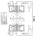
- FIG. 3 illustrates two Hall-Current ion sources 200 and 202 with features similar to those of FIG.1 which are arranged to treat both sides of workpiece 210.
- the Hall-Current ion sources are independently powered by power supplies 220 and 222 and each have their own self-sustained cathode 230 and 232.
- each ion source electromagnet 240 and 242 are driven by separate AC power supplies 244 and 246.
- This dual-sided configuration is particularly useful in treating or coating both sides of substrate or fixture 210 simultaneously.
- One example of the utility of this configuration is in the deposition of DLC and Si-DLC coatings simultaneously on both sides of magnetic disks.
- the substrate may consist of metal, a semiconductor, ceramic, glass, polymers, or combination thereof that may or may not include an adhesion-enhancing interlayer for the DLC or Si-DLC coating.
- such a layer may be deposited by the Hall-Current ion source apparatus or by any conventional alternative means within or outside the vacuum chamber prior to deposition of the DLC or Si-DLC coating.
- the process for deposition of the DLC or Si-DLC coating is principally controlled by a combination of (1) source-to-substrate spacing and orientation, (2) anode current, voltage or power, (3) electromagnet current or the amp-turns within the electromagnet, (4) plasma maintenance gas flow, (5) precursor gas composition, and (6) precursor gas flow rate.
- the anode current and anode voltages are not independent when conventional hollow cathode electron sources are used.
- anode current and potential can be decoupled by using hot filament-assisted hollow cathode electron sources, such as that described by Fedoseev et al.
- electron emission from this type of cathode may be used to control anode voltage (power) independently through the control of cathode electron injection into anode discharge region against the rate of charged particle generation within the anode discharge region.
- Thickness and deposition rate of DLC and Si-DLC coatings were determined from profilometry measurements performed on a Tencor P-10 Profilometer. Stress measurements were determined from films on 100 mm diameter Si stress wafers by means of a Frontier Semiconductor Measurements FSM 8800 Film Stress Measurement Machine. Measurements of Nanoindentation hardness were taken by a Nano Instruments Inc. Nanoindenter II on DLC and Si-DLC coatings with thickness greater than about 250nm (2500 ⁇ ).
- a Hall-Current ion source similar to that depicted in FIG. 1 with nominal anode gap diameter of 7.6 cm was used to deposit DLC coatings.
- the electromagnet of the ion source was powered by means of the anode discharge current.
- a 100 mm diameter silicon wafer substrate was located 18 cm from the face of the ion source. Prior to deposition the Si sample surfaces were sputter-cleaned using a beam of argon ions generated by a secondary ion source before being rotated into the beam of the depositing ion source.
- DLC coatings were deposited by operating the ion source with argon and methane gases.
- Argon plasma maintenance gas was introduced through the anode gap of the ion source at flow rates from about 20 to 40 sccm.
- Methane precursor gas was introduced at total flow rates from about 60 to 100 sccm, and equally distributed through four 0.64 cm o. d. metal nozzles that were symmetrically disposed about the outer diameter of anode discharge region and at about 1 cm from the face of the ion source.
- vacuum pressures ranged from about 53 to 107 mPa (0.4 to 0.8 mTorr), the anode currents of ranged from about 7 to 9 Amps, and the anode voltage from about 120 to 150 Volts.
- Profilometry measurements indicated that the average deposition rates for the DLC coatings were in the range of 1.4 to 2nm (14 to 20 ⁇ ) per second.
- the compressive stress and Nanoindentation hardness of the DLC coatings were in the range of about 1 to 1.5 GPa (1 to 1.5 x10 10 dynes/cm 2 ), and about 12 to 14 GPa, respectively.
- Example A The same Hall-Current ion source used in Example A was used to deposit DLC coatings by operating the ion source with argon and acetylene gases. In this example, however, the electromagnet of the ion source was powered by means of an AC power supply.
- a 10 to 20nm (100 to 200 ⁇ ) thick layer of Si-DLC was deposited as an adhesion-enhancing interlayer prior to deposition of the 250 to 500nm (2500 to 5000 ⁇ ) thick, highly stressed DLC coatings.
- the thin layer of Si-DLC was deposited by flowing tetramethylsilane precursor gas through the nozzles.
- argon plasma maintenance gas was introduced through the anode gap of the ion source at flow rates from 15 to 25 sccm, and acetylene precursor gas was introduced through the nozzles at total flow rates from 40 to 80 sccm.
- vacuum pressures ranged from about 53 to 107 mPa (0.4 to 0.8 mTorr), the rms anode current levels of ranged from 5 to 11 Amps, and the anode voltage from 60 to 100 Volts.
- Profilometry measurements indicated that the average deposition rates for the DLC coatings were in the range of 0.8 to 2.3nm (8 to 23 ⁇ ) per second.
- the compressive stress and Nanoindentation hardness of the DLC coatings were in the range of about 0.4 to 3.8 GPa (0.4 to 3.8 x10 10 dynes/cm 2 ), and about 11 to 22 GPa, respectively.
- Example A The same Hall-Current ion source configuration used in Example A was used to deposit DLC coatings by operating the ion source with argon and 1,3-butadiene gases.
- Example B the electromagnet of the ion source was powered by means of an AC power supply.
- Example B a 10 to 20nm (100 to 200 ⁇ ) thick layer of Si-DLC was deposited as an adhesion-enhancing interlayer prior to deposition of the highly stressed DLC coatings.
- argon plasma maintenance gas was introduced through the anode gap of the ion source at flow rates from 15 to 25 sccm, and butadiene precursor gas was introduced through the nozzles at total flow rates from 30 to 60 sccm.
- vacuum pressures ranged from about 53 to 107 mPa (0.4 to 0.8 mTorr), the rms anode current levels of ranged from 5 to 11 Amps and the anode voltage from 60 to 100 Volts.
- the compressive stress and Nanoindentation hardness of the DLC coatings were in the range of about 0.7 to 2.7 GPa (0.7 to 2.7 x10 10 dynes/cm 2 ), and about 10 to 18 GPa, respectively.
- Example B The same Hall-Current ion source used in Example B was used to deposit DLC coatings by operating the ion source with argon and acetylene gases. In this example, however, the Si wafer substrates were located at distances of about 10 cm and about 18 cm from the face of the ion source.
- argon plasma maintenance gas was introduced through the anode gap of the ion source at flow rate of 50 sccm, and acetylene precursor gas was introduced through the nozzles at total flow rates from 10 to 80 sccm.
- vacuum pressures ranged from about 67 to 93 mPa (0.5 to 0.7 mTorr), the rms anode current levels of ranged from 10 to 12 Amps and the anode voltage from 60 to 100 Volts.
- the compressive stress and Nanoindentation hardness of the DLC coatings were in the range of about 0.3 to 4.5 GPa (0.3 to 4.5 x10 10 dynes/cm 2 ), and about 2 to 25 GPa, respectively.
- the DLC deposition rate and Nanoindentation hardness as a function of acetylene precursor gas flow rate (10 to 80 sccm) for anode currents of 10 Amps and 12 Amps and a source-to-substrate distance of 10 cm are presented in FIG. 4 and FIG. 5 , respectively.
- This example illustrates the deposition of a layer of Si-DLC using the Hall-Current ion source.
- the Si-DLC material was utilized as an adhesion-enhancing interlayer between the substrate and a top coating layer of DLC.
- This multilayer coating process has been demonstrated to produce highly adherent thick DLC coatings using the Hall-Current ion source, which DLC coatings have a compressive stress in the range of about 1 to 4 GPa (1 x10 10 to 4x10 10 dynes/cm 2 ).
- Example A The same Hall-Current ion source used in Example A was used to deposit Si-DLC and DLC coatings by operating the ion source with argon, tetramethylsilane (TMS) and acetylene gases. During coating deposition, argon plasma maintenance gas was introduced through the anode gap of the deposition ion source, and the precursor gases (TMS and acetylene) were introduced via nozzles as in Example A.
- TMS tetramethylsilane
- acetylene gases argon plasma maintenance gas was introduced through the anode gap of the deposition ion source, and the precursor gases (TMS and acetylene) were introduced via nozzles as in Example A.
- the electromagnet of the ion source was powered by means of an AC power supply.
- a 100 mm diameter silicon wafer substrate was located about 18 cm from the face of the ion source. Prior to deposition the Si sample surfaces were sputter-cleaned by a secondary ion source before being rotated into the beam of the depositing ion source.
- Three coating layers were deposited to comprise the multilayer DLC coating:(1) a first Si-DLC coating interlayer having the highest atomic concentration of Si, (2) a second Si-DLC coating interlayer having a low atomic concentration of Si, and (3) a top coating layer of DLC. Some coatings were attempted without a Si-DLC adhesion layer, i. e. only step (3) was performed.
- the flow rate of Ar plasma maintenance gas through the anode was 18 sccm, and the flow rate of TMS precursor gas through the nozzles was 7 sccm.
- the vacuum chamber pressure was about 40 mPa (0.3 mTorr), the rms anode currents ranged from 9 to 11 Amps, and the rms anode voltage ranged from about 80 to 90 Volts.
- the deposition time for the first layer of Si-DLC was about 30 seconds.
- the flow rate of Ar plasma maintenance gas through the anode was 18 sccm, and the precursor gas feed was comprised of 7 sccm of TMS plus 60sccm of acetylene.
- the vacuum chamber pressure was about 93 mPa (0.7 mTorr), the rms anode currents ranged from 9 to 11 Amps, and the rms anode voltage ranged from about 70 to 80 Volts.
- the deposition time for the first layer of Si-DLC was about 15 seconds.
- the flow rate of Ar plasma maintenance gas through the anode was 18 sccm, and the precursor gas feed was 60sccm of acetylene.
- the vacuum chamber pressure was about 53 mPa (0.4 mTorr), the rms anode currents ranged from 9 to 11 Amps, and the rms anode voltage ranged from about 80 to 90 Volts.
- the deposition time for the first layer of Si-DLC was about 140 seconds.
- DLC coatings prepared with only step (3) did not adhere well to the silicon substrates as indicated by a tape pull dry adhesion test and isopropyl alcohol wipe test. In fact, areas of these coatings began to delaminate before removing the specimen from the vacuum chamber. However, all coatings prepared by steps (1) through (3) passed the tape pull and isopropyl alcohol wipe tests for adhesion.
- This example illustrates the deposition of a single layer of Si-DLC using the Hall-Current ion source.
- the required characteristics of the coating are provided by the Si-DLC coating alone, with the need for deposition of a top layer of DLC.
- Example B The same Hall-Current ion source used in Example B was used to deposit Si-DLC coatings by operating the ion source with argon and TMS gases. In this example, however, the 100 mm diameter Si wafer substrates were located at a distance of about 10 cm from the face of the ion source.
- the Si sample surfaces Prior to deposition the Si sample surfaces were sputter-cleaned by Ar ion beam etching using the Hall-Current ion source operated on Ar gas only.
- argon plasma maintenance gases were introduced through the anode gap of the ion source at flow rate of 50 sccm, and TMS precursor gas was introduced through the nozzles at total flow rate of 7 sccm.
- the vacuum chamber pressure was about 67 mPa (0.5 mTorr), the rms anode currents ranged from 7 to 10 Amps, and the rms anode voltage ranged from about 50 to about 75 Volts.
- the deposition times for the Si-DLC coatings were in the range of about 240 to 300 seconds.
- Profilometry measurements of the Si-DLC coatings indicated coating thicknesses in the range of 190 to 210 nm (1900 to 2100 ⁇ ), with average deposition rates ranging from about 1.2 to 1.6nm (12 to 16 ⁇ ) per second.
- the compressive stress and Nanoindentation hardness of the Si-DLC coatings were in the range of about 2.0 to 2.3 GPa (2.0 to 2.3 x 10 10 dynes/cm 2 ), and about 17 to 18 GPa, respectively, for the conditions studied.
- Examples G-K present the results of a series of experiments in which a closed-drift Hall-Current ion source of the present invention was utilized to produce DLC coatings for application on magnetic hard disks used in magnetic data storage.
- Example L demonstrates an embodiment for producing DLC coatings of extremely high hardness using a closed-drift Hall-Current ion source of the present invention.
- Example M demonstrates another embodiment of the present invention in which a non-closed drift Hall-Current ion source of the present invention having an anode channel of rectangular cross-section is used to deposit DLC coatings.
- This ion source configuration is suitable for depositing DLC coatings on magnetic hard disks in large in-line deposition systems in which large pallets of disks are continuously passed in front of the ion source.
- the ion source is suitable for deposition of DLC and Si-DLC onto large area substrates such as sheets of plastic, glass or metal, or other large substrates as well.
- the examples further show that the process of the present invention can deposit DLC coatings onto magnetic hard disks at a high deposition rate suitable for mass production in two modes.
- substrates are coated as they are continuously passed through the carbon-containing plasma ion beam generated by a continuously operating Hall-Current ion source.
- pulsesed static deposition mode as illustrated in Examples H and J, individual substrates are coated one at a time as they are sequentially moved in front of the ion source.
- the deposition flux is pulsed on after the substrate has been positioned in front of the ion source, the deposition flux is pulsed off after the deposition of the appropriate thickness of the DLC coating, then the substrate is removed from the DLC deposition zone.
- the precursor gas flow was introduced into the plasma beam in front of the ion source via nozzles made of metal tubing.
- Three nozzle configurations were used in the experiments.
- the first nozzle configuration four nozzle tubes, oriented in a plane parallel to and approximately 6.35mm (0.25 inch) downstream of the face of the ion source were used.
- the nozzles were oriented 90 degrees from each other and pointed radially inward toward the center of the ion source.
- the end of each nozzle was located approximately 6.35mm (0.25 inch) from the outer diameter of the annular anode channel. This position is noted as the "IN" position in data Tables 1-4 below.
- the second nozzle configuration was similar to the first, except that the end of each nozzle was located approximately 25.4mm (1 inch) from the outer diameter of the annular anode channel. This position is noted as the "OUT" position in data Tables 1-5 below.
- the third nozzle configuration was similar to the first, except that the nozzles were oriented to deliver the flow of precursor gas across the discharge zone, in a direction along a line tangential to the circle describing the center of the annular anode. This position is noted as the "SIDE" position in Table 1. In all these experiments, the hydrocarbon precursor gas flow was split equally among each of the four nozzles.
- the vacuum chamber was pumped down to approximately 1.3 mPa (1 x 10 -5 Torr) or less prior to initiating the DLC deposition process.
- precursor gas flows ranging from about 2 sccm to about 500 sccm can be used with the ion source of Example B. Higher precursor gas flows increase the background pressure in the deposition chamber. Larger pumping capacity allows higher gas flows to be used while maintaining the total pressure below the desired maximum pressure of about 1.3 Pa (10milliTorr).
- Argon plasma maintenance gas was fed through the source for all the deposition runs. It was determined that the sum of the argon flow and the hydrocarbon precursor gas flow needed to be above approximately 35 sccm for optimal operation of the particular ion source used in Examples G, H, I and J. This minimum flow is dependent on the ion source operating parameters as well as the background pressure which is controlled by pumping capacity.
- the vacuum chamber pressure during DLC deposition was measured with a capacitance manometer.
- the indicated pressure as presented in data Tables 1-4 was about 66mPa (0.5milliTorr) higher when the ion source plasma was turned off, indicating a significant amount of consumption of the hydrocarbon precursor gas by the deposition process.
- the deposition chamber used for the experiments had the capability to throttle the speed of the high vacuum pump, allowing for a comparison of results obtained at similar gas flow rates, but different chamber pressures.
- the deposition tests were conducted using anode currents (ion source plasma discharge current) which range was smaller than the total operating range of the ion source.
- the anode power supply was run in the current control mode, such that the anode voltage would automatically stabilize at the value required to achieve the desired anode current setting.
- the resulting anode voltage for a particular anode current setting was a function of the gas flow rate, chamber pressure, nozzle position, the magnetic field in the plasma region of the ion source, and geometrical arrangement of the ion source, substrate, and the vacuum chamber.
- the magnetic field within the ion source was induced by an electromagnet, which was operated with an independent 60 Hz AC current supply.
- Examples G, H, I and J utilized the following range of process parameters for the deposition of DLC coatings:
- the desired thickness of the ion beam deposited DLC coating is in the range of about 2 to 10nm (20 ⁇ to 100 ⁇ ).
- the thickness of the DLC coating on the magnetic disks was often made thicker, up to about 80nm (800 ⁇ ).
- DLC coatings having thickness up to 710nm (7100 ⁇ ) were deposited on silicon wafers for measurement of mechanical properties such as compressive stress and Nanoindentation hardness.
- the deposited DLC coatings were characterized by Nanoindentation hardness of greater than 10 GPa, compressive stress greater than 0.5 GPa, and Raman G-peak position greater than 1500cm -1 , and Raman background (luminescence) slope generally greater than 1.
- the first test condition used ambient conditions of approximately 20°C to 25°C room temperature and 30% to 50% relative humidity.
- the second type of CSS test used conditions known to be very aggressive for magnetron sputtered carbon coatings: elevated temperature of 55°C and 5% relative humidity. The friction coefficient of the DLC coating was measured before and after each test.
- DLC coatings were deposited onto Si wafers and magnetic hard disks with the Hall-Current ion source of Example B using acetylene or 1,3-butadiene as the hydrocarbon precursor gas.
- a matrix of deposition runs was designed to examine the effect of ion source process parameters on the resulting DLC material properties.
- the thickness of the DLC coatings was chosen to be in the range of about 270nm to 710nm (2700 ⁇ to 7100 ⁇ ), which was optimum for characterization of mechanical properties such as compressive stress and Nanoindentation hardness.
- the ion source plasma was first stabilized for several minutes by operation on argon plasma maintenance gas only. Then, the first substrate was moved into position in front of the source, and exposed to a beam of argon ions to sputter-etch the surface for approximately 10 to 20 seconds. Then, the hydrocarbon precursor gas was added, and the ion source parameters were adjusted to the desired settings for deposition of DLC.
- the DLC deposition process was then continued for a time of 15 seconds to 20 minutes to achieve the final thickness values shown in Tables 1 and 2. No adhesion layer between the substrate and the DLC coatings was used.
- the substrate was rotated out of the ion beam while the ion beam remained on and the precursor gas was still flowing; i. e. the ion source was still depositing DLC. (Note that the ion beam was never started or stopped when the substrate was in front of the source; i. e. the substrate was continually exposed to the ion beam when it was in front of the ion source.) Then, the precursor gas flow was shut off and an argon ion beam was reestablished without shutting off the ion source plasma. Then, the next substrate was rotated into the argon ion beam, and the aforementioned process steps for sputter-etching and DLC deposition were repeated.
- the results in Table 1 show that the process of the present invention utilizing 1,3-butadiene precursor gas is capable of depositing DLC coatings at a deposition rate up to at least 4.7nm (47 ⁇ ) per second, and hardness up to at least 22.5 GPa.
- the results in Table 2 show that the process of the present invention utilizing acetylene precursor gas is capable of depositing DLC coatings at a deposition rate up to at least 3.5 nm (35 ⁇ ) per second, and hardness up to at least 26.6 GPa.
- the deposition rate would be even greater if the distance between the ion source and the substrate was further reduced, or if higher flow rates of hydrocarbon precursor gas were utilized (see FIG. 4 ).
- Example G The same ion source used in Example G was used to deposit DLC coatings, but via pulsed deposition mode in which the carbon-containing deposition flux was turned on and off repeatedly during deposition.
- the carbon-containing deposition flux was pulsed on and off either by (i) pulsing the anode power supply with argon plasma maintenance gas and hydrocarbon precursor gas continuously flowing, or (ii) pulsing the hydrocarbon precursor gas flow with the plasma maintenance gas continuously flowing and the anode power supply continuously on.
- the thickness of the DLC coatings was in the range of about 350nm to 610nm (3500 ⁇ to 6100 ⁇ ), which allowed for characterization of mechanical properties such as compressive stress and Nanoindentation hardness.
- the thickness of the DLC coatings in the deposition runs on magnetic disks wafers was in the range of 40nm to 80nm (400 ⁇ to 800 ⁇ ), which was chosen for ease of Raman spectroscopy characterization of the DLC material while maintaining good adhesion of the DLC coatings to the magnetic disk substrates.
- Pulsing the precursor gas also tends to produce a harder DLC coating than pulsing the plasma power supply.
- the DLC hardness produced by the pulsed anode current method is somewhat lower than that obtained by continuous operation, and the DLC hardness produced by the pulsed precursor gas method is somewhat higher than that obtained by continuous operation.
- DLC coatings of thickness in the range of about 5 to 7nm (50 to 70 ⁇ ) were deposited on 95 mm diameter magnetic hard disks in pass-by mode using the ion source and substrate fixturing configuration of Example G.
- the substrates were prepared by a standard manufacturing process used to make commercial hard disks, except that the process was interrupted prior to the application of the standard magnetron sputtered carbon overcoat.
- the DLC deposition runs summarized in Table 4 below, utilized 1,3-butadiene as the hydrocarbon precursor gas.
- the distance between the source and disk substrate was 177.8mm (7 inches).
- the disks After application of the DLC coating, the disks received standard post-deposition processing steps of burnishing and lubing. Selected disks were then tested to verify the performance of these ultrathin DLC coatings of the present invention.
- the disks coated in each of the runs summarized in Table 4 below all passed 20,000 CSS cycles under ambient conditions, and 10,000 CSS cycles under aggressive conditions of elevated temperature, e.g. 55°C, and low humidity, i. e. 5%, indicating outstanding performance.
- the performance of these disks coated with about 5 to 7nm (50 to 70 ⁇ ) of DLC by the process of the present invention was greatly superior to that obtained with magnetron sputtered carbon overcoats.
- DLC coatings of thickness in the range of about 5 to 7 nm (50 to 70 ⁇ ) were prepared on 95 mm diameter magnetic hard disks as described in Example I, but the deposition was carried out in pulsed static mode.
- the DLC deposition was started and stopped only by pulsing the flow of precursor gas while the ion source remained operating with argon plasma maintenance gas.
- the ion source plasma and ion beam were first stabilized by operation on argon plasma maintenance gas only. Then, a disk substrate was rotated into position in front of the ion source.
- the hydrocarbon precursor gas was pulsed on, and remained on for a time sufficient to deposit a DLC coating with target thickness between 5 nm and 7 nm (50 ⁇ and 70 ⁇ ). After completion of this deposition time, the precursor gas flow was turned off. Then, the disk was moved to a position away from the source.
- the DLC deposition was started by pulsing on the flow of precursor gas while the ion source remained operating with argon plasma maintenance gas, but the deposition was stopped by turning off the anode power supply to extinguish the ion source plasma.
- the ion source plasma and ion beam were first stabilized by operation on argon plasma maintenance gas only. Then, the disk was rotated into position in front of the ion source.
- the hydrocarbon precursor gas was pulsed on, and remained on for a time sufficient to deposit a DLC coating with target thickness between 5 nm and 7 nm (50 ⁇ and 70 ⁇ ).
- the anode power supply was turned off to extinguish the ion source plasma and the ion beam.
- the disk was moved to a position away from the source.
- the source was restarted on argon plasma maintenance gas as noted above, and the same process was continued on other substrates.
- the DLC deposition runs summarized in Table 5 below utilized 1,3-butadiene or acetylene as the hydrocarbon precursor gas.
- Disks coated in each of the runs summarized in Table 5 passed 20,000 CSS cycles under ambient conditions, and 10,000 CSS cycles under aggressive conditions of elevated temperature and low humidity, indicating outstanding performance. As in Example I, it was found that the performance of these disks coated with about 5 to 7 nm (50 to 70 ⁇ ) of DLC by the process of the present invention was greatly superior to that obtained with magnetron sputtered carbon overcoats of similar thickness.
- Table 5 Run Mode A(I) A(V) M(I) B fld. Gas HC Cnfg. Ar Thk.
- Closed-drift Hall Current ion sources similar to the source used in Example G were used to deposit DLC coatings as the protective layer on magnetic disks using a fully automated manufacturing process in an Intevac MDP-250B production magnetic disk coating system.
- the ion sources were flange-mounted as illustrated in FIG. 2 .
- the Intevac MDP-250B system utilized three separate chamber stations to deposit a magnetron sputtered carbon overcoat as the protective layer on magnetic disks as they passed through the machine. Each station housed two opposing magnetron cathodes, which were configured to simultaneously coat both sides of each magnetic disk. Because of the low deposition rate of magnetron sputtered carbon, three sputter deposition stations were necessary to meet the high production throughput requirements of the machine.
- the magnetron sputtering sources and related support equipment were removed from the three stations on the machine.
- two flange-mounted Hall-Current ion sources of the present invention were mounted in place of the magnetron sputtering sources, resulting in a configuration as in FIG. 3 , so that both sides of the disk were simultaneously coated with ion beam DLC.
- This station was also modified to add an additional port for pumping by a 2,000 l/second turbopump.
- argon plasma maintenance gas was continuously flowed through source during the entire process cycle which involved (1) disk transfer into the DLC coating station from the previous station, (2) DLC deposition, and (3) disk transfer out of the DLC station into the next station.
- DLC deposition was performed by flowing C 2 H 2 gas through nozzles in front of the source for a predetermined time to achieve the desired DLC coating thickness. No adjustments were made to other source parameters when the C 2 H 2 was introduced except in a few cases when the Ar plasma maintenance gas was also lowered slightly. This process was essentially the equivalent of the "first pulsed mode process" described in Example J.
- DLC coatings were deposited on disks for CSS testing using the following conditions in each source:
- Magnetic disks coated with 5nm (50 ⁇ ) ion beam DLC made under eight different conditions within and including the ends of these ranges, each passed 20,000 CSS test cycles under ambient conditions and 10,000 CSS test cycles under aggressive conditions of elevated temperature and low humidity, indicating outstanding performance.
- DLC coatings 400nm (4000 ⁇ ) thick DLC coatings were deposited on silicon substrates in a similar process to that used for the magnetic disks, except the heat and metal layer processes were not performed prior to the DLC coating. DLC coatings were deposited using the following conditions in each source:
- Example A The same Hall-Current ion source used in Example A was used to deposit DLC coatings by operating the ion source with argon and acetylene gases. In this example, however, the anode and electromagnet of the ion source were powered by means of separate DC power supplies. The deposition conditions and results are presented in Table 6. The DLC deposition runs summarized in Table 6 were all performed on silicon wafer substrates, using acetylene as the hydrocarbon precursor gas, and nozzle configuration in the IN position.
- a non-closed drift Hall-Current ion source having a linear anode configuration similar to that shown in FIG. 4A of the Mahoney et al. co-pending patent application U. S. Ser. No. 08/901,036 was used to deposit DLC coatings.
- the anode was about 0.8m (30 inches) long, and the anode channel was approximately 12.7mm (0.5 inch) deep and 12.7mm (0.5 inch wide).
- Twenty-eight electromagnet coils operated on 60 cycle AC current were used to induce a magnetic field across the anode between the two magnetic poles that extended along each side of the anode. The ends of the anode channel were closed off with an insulating material.
- Argon plasma maintenance gas was fed from the back of the source and emerged through the shadowed anode gap along the center line of the anode.
- Two hollow cathode electron sources mounted near the ends of the anode, were used to supply the electrons to maintain the plasma.
- acetylene precursor gas was introduced into the ion beam via 4 nozzles mounted along the length of the anode channel. Each nozzle directed a stream of precursor gas across the ion beam approximately perpendicular to the long dimension of the anode.
- the nozzles were mounted approximately 177.8mm (7 inches) apart and were spaced approximately 6.35mm (0.25 inch) downstream of the face of the ion source.
- the long dimension of the ion source was mounted in a vertical orientation, and the ion beam was directed horizontally at four 101.6mm (4-inch) diameter Si wafer substrates.
- the substrates were placed about 177.8mm (7 inches) downstream from the front of the ion source and parallel to the face of the source.
- the center of each substrate wafer lined up directly in front of the center of the anode channel and directly in front of one of the four hydrocarbon nozzles.
- the chamber was evacuated to pressure of less than 1.3mPa (1 x 10 -5 Torr).
- the ion source plasma was initiated on argon and allowed to stabilize.
- DLC deposition was initiated by flowing 10sccm of acetylene precursor gas through each nozzle.
- a DLC coating was deposited onto the substrates in Run #1014L using the following conditions: anode voltage between 100 and 111 Volts; anode current of 40 Amps; magnet current of 4 Amps through each of the 28 electromagnets, magnetic field of approximately 15mT (150 Gauss); argon plasma maintenance gas flow rate of 140 sccm, total acetylene precursor gas flow rate of 40sccm; chamber pressure during deposition of approximately 213mPa (1.6mTorr); deposition time of 4 minutes. Upon completion of the deposition, the vacuum chamber was vented, and the DLC-coated substrate was recovered.
- the maximum thickness of the DLC coating was 164.5nm (1645 ⁇ ), corresponding to a deposition rate of approximately 0.7nm (7 ⁇ ) per second.
- the coating compressive stress was between about 3 and 3.8 GPa.
- the film was too thin to obtain accurate Nanoindentation hardness measurements, but based on the known correlation between compressive stress and hardness for other DLC films deposited from acetylene precursor gas with Hall-Current ion sources of the present invention, the coating hardness was expected to be in the range of about 19 to 23 GPa.
- DLC coatings were ion beam deposited using the linear anode, non-closed drift Hall-Current ion source of Example M, except that both the argon plasma maintenance gas and the acetylene precursor gas were both introduced through the shadowed anode gap directly into the plasma discharge.
- the ⁇ 101.6mm (4-inch) diameter Si wafer substrates were placed about 177.8nm (7 inches) downstream from the front of the ion source and parallel to the face of the source.
- DLC coatings were deposited using the following conditions: anode voltage between 93 and 103 Volts; anode current in the range of 36 to 40 Amps; magnet current of 4 to 8 Amps through each of the 28 electromagnets; magnetic field of approximately 15 to 30 mT (150 to 300 Gauss); argon plasma maintenance gas flow rate of 180 to 200 sccm; acetylene precursor gas flow rate of 50 to 60sccm; chamber pressure during deposition of approximately 240 to 253mPa (1.8 to 1.9mTorr).
- the resulting DLC coatings had thickness in the range of 198 to 520nm (1980 to 5200 ⁇ ), corresponding to deposition rates in the range of approximately 0.3 to 0.9nm (3 to 9 ⁇ ) per second.
- the compressive stress of the coatings was in the range of 1 to 3.8 GPa, and the Nanoindentation hardness of the coatings was in the range of 13 to 22 GPa.
- Run#1120L the deposition conditions were similar, but the distance between the source and substrates was reduced from 177.8mm (7 inches) to ⁇ 52.4mm (6 inches).
- the compressive stress of the DLC coating deposited was 4.5 GPa, with anticipated hardness of about 25 GPa.
- Examples A-N above demonstrate the unexpectedly high rate of deposition (typically greater than 1nm (10 ⁇ ) per second) of very hard (greater than 10 GPa) DLC and Si-DLC coatings using the Hall-Current ion source process of the present invention.
- the prior art suggests that such high hardness materials require an ion beam deposition system which delivers 100 eV per C atom deposited.
- an ion beam with mean beam energy of 150 to 250 eV would be required to deposit very hard DLC coatings from acetylene, which in a low pressure plasma state principally forms C 2 H x + ions.
- the preceding examples show that high hardness DLC and Si-DLC coatings can be formed with the high density ion beams formed by the process of the present invention with mean time-averaged energies that are substantially lower than the 100 eV per C atom criterion.
- the preceding examples also illustrate the ability of the unique Hall-Current ion source apparatus to deposit very hard DLC coatings at high rates in a manner that cannot be deduced from prior art gridless Hall-Current ion sources and related teachings.
- the characteristics of high deposition rate and high coating hardness make the process of the present invention ideal for the production of thin DLC and Si-DLC coatings for key industrial applications including: data storage or recording media such as magnetic hard disks, floppy disks and magnetic tape; magnetic transducers used in magnetic recording such as magnetoresistive sliders and tape heads; optical data storage disks utilizing phase-change media; production of barrier coatings for packaging, pharmaceutical and chemical applications; antireflection, filter and bandpass optical coatings; and wear-resistant, corrosion-resistant, and abrasion-resistant protective coatings for a variety of substrates consisting of metal, ceramic, glass, plastics and their combinations.
Landscapes
- Chemical & Material Sciences (AREA)
- Mechanical Engineering (AREA)
- Organic Chemistry (AREA)
- Chemical Kinetics & Catalysis (AREA)
- Engineering & Computer Science (AREA)
- Materials Engineering (AREA)
- General Chemical & Material Sciences (AREA)
- Metallurgy (AREA)
- Inorganic Chemistry (AREA)
- Health & Medical Sciences (AREA)
- Toxicology (AREA)
- Chemical Vapour Deposition (AREA)
- Manufacturing Of Magnetic Record Carriers (AREA)
- Carbon And Carbon Compounds (AREA)
- Physical Vapour Deposition (AREA)
Claims (19)
- Verfahren zur Abscheidung einer Beschichtung aus diamantartigem Kohlenstoff (DLC-Beschichtung) auf der Oberfläche eines Substrats unter Verwendung einer Hall-Effekt-Ionenquelle, umfassend die Schritte:(a) Befestigen dieses Substrats in einer Abscheidungsvakuumkammer, die eine Hall-Effekt-Ionenquelle enthält, und Auspumpen der Luft aus dieser Kammer;(b) Zuführen eines Inertgases zu mindestens einer selbständigen Kathodenelektronenquelle dieser Hall-Effekt-Ionenquelle und Anregen dieser Kathodenelektronenquelle, um eine Zufuhr von Elektronen zu einer Anode dieser Hall-Effekt-Ionenquelle bereitzustellen, wobei diese Anode von dieser Vakuumkammer derart elektrisch isoliert ist, dass die Bildung eines Plasmas, das in das Innere dieser Hall-Effekt-Ionenquelle wandert, hinter dieser Anode verhindert wird, wobei diese Anode eine Spalte aufweist, die so konfiguriert ist, um im Wesentlichen die Sichtlinienabscheidung der Beschichtung auf die Anode innerhalb der Spalte zu beschränken;(c) Einführen von Plasmaaufrechterhaltungsgasen durch diese Spalte dieser Anode und in einen Anodenentladungsbereich innerhalb dieser Vakuumkammer und Anlegen einer Spannung, um einen Anodenentladungsstrom bereitzustellen, der zwischen dieser Anode und dieser Elektronenquelle fließt, wobei ein durch elektromagnetische Mittel erzeugtes magnetisches Feld über diesem Anodenentladungsbereich gebildet wird und Elektronen die Plasmaaufrechterhaltungsgase ionisieren, um einen Plasmastrahl von Gasionen in diesem gesamten Anodenentladungsbereich zu bilden;(d) Abscheiden durch Plasmaionenstrahl einer Schicht von DLC aus kohlenstoffhaltigen Vorläufergasen unter Verwendung dieses Plasmastrahls, während diese Anode durch andere Kühlmittel als strahlende thermische Emission thermisch gekühlt wird,(e) Erhöhen des Vakuumkammerdrucks auf Atmosphärendruck und(f) Gewinnen eines DLC-beschichteten Substratprodukts.
- Verfahren nach Anspruch 1, in welchem die Beschichtung aus diamantartigem Kohlenstoff eine Beschichtung aus siliciumdotiertem diamantartigem Kohlenstoff (Si-DLC) ist und die Vorläufergase kohlenstoffhaltige und siliciumhaltige Vorläufergase enthalten.
- Verfahren nach Anspruch 1 oder 2, wobei der Anodenentladungsstrom, der zwischen dieser Anode und dieser Kathodenelektronenquelle fließt, zumindest teilweise diese elektromagnetischen Mittel antreibt.
- Verfahren nach einem der vorstehenden Ansprüche umfassend alternierende Stromkreiseinrichtungen, um zumindest teilweise diese elektromagnetischen Mittel anzutreiben und um die Richtung der Flusslinien des magnetischen Felds dieser elektromagnetischen Mittel periodisch umzukehren.
- Verfahren nach einem der vorstehenden Ansprüche, wobei die Richtung der Flusslinien des durch diese elektromagnetischen Mittel erzeugten magnetischen Feldes im Wesentlichen parallel zu der Oberfläche dieser Anode am zweiten Ende dieses Anodenentladungsbereichs verläuft.
- Verfahren nach einem der vorstehenden Ansprüche, wobei die Richtung der Flusslinien des durch diese elektromagnetischen Mittel erzeugten magnetischen Feldes in eine Richtung, die im Wesentlichen die gleiche wie die des Plasmastrahls, der aus diesem Anodenentladungsbereichs austritt, ist, divergiert.
- Verfahren nach einem der vorstehenden Ansprüche, wobei diese Kathodenelektronenquelle achsensymmetrisch in Bezug auf diesen Anodenentladungsbereich angeordnet ist.
- Verfahren nach einem der vorstehenden Ansprüche, wobei die Plasmaaufrechterhaltungsgase im Wesentlichen einheitlich durch diese Spalte in der Anode aus Eindüsmitteln und in diesen Anodenentladungsbereich verteilt werden und der resultierende Anodenentladungsstrom im Wesentlichen einheitlich benachbart zu dieser Spalte verteilt wird.
- Verfahren nach einem der vorstehenden Ansprüche, wobei die Dimensionen des Spaltes innerhalb dieser Anode mindestens größer als die charakteristische Debye-Länge des lokalen Plasmas, das nahe der Spalte in dieser Anode gebildet wird, sind, so dass dieser Anodenentladungsstrom im Wesentlichen an dieser Anode innerhalb der Spalte nahe eines lokalisierten Bereichs, in dem die Plasmaaufrechterhaltungsgase in diesen Anodenentladungsbereich eintreten, aufrechterhalten wird.
- Verfahren nach einem der vorstehenden Ansprüche, wobei Verteilermittel in diesem Gehäuse eingeschlossen sind, um diese Vorläufergase direkt in den Plasmastrahl und getrennt von den Eindüsmitteln zur Einführung der Plasmaaufrechterhaltungsgase durch diese Spalte einzuführen.
- Verfahren nach Anspruch 10, wobei diese Verteilermittel mindestens eine Röhre mit einer Düse an einem Ende zum Leiten der Vorläufergase in diesen Anodenentladungsbereich aufweisen.
- Verfahren nach Anspruch 10, wobei diese Verteilermittel mindestens einen Verteilerring zum Leiten des Abscheidungsgases in diesen Anodenentladungsbereich aufweisen.
- Verfahren nach Anspruch 10, wobei diese Verteilermittel mindestens eine Röhre mit einer Düse an einem Ende zum Leiten der Vorläufergase aus diesem Anodenentladungsbereich heraus aufweisen.
- Verfahren nach Anspruch 10, wobei diese Verteilermittel mindestens einen Verteilerring zum Leiten der Vorläufergase aus diesem Anodenentladungsbereich heraus aufweisen.
- Verfahren nach einem der vorstehenden Ansprüche, wobei der Strom dieser Vorläufergase während der Abscheidung durch Plasmaionenstrahl gepulst wird und dieses Plasmaaufrechterhaltungsgas kontinuierlich durch diese Spalte eingeführt wird.
- Verfahren nach einem der Ansprüche 1 bis 15, wobei diese kohlenstoffhaltigen Vorläufergase kontinuierlich während der Abscheidung durch Plasmaionenstrahl eingeführt werden und dieser Anodenentladungsstrom gepulst wird.
- Verfahren nach einem der vorstehenden Ansprüche, wobei dieses Substrat in dieser Abscheidungsvakuumkammer so montiert ist, dass beide Seiten des Substrats gleichzeitig beschichtet werden.
- Verfahren nach einem der vorstehenden Ansprüche, wobei Spannung an diese Anode und an diese elektromagnetischen Mittel durch getrennte Gleichstromquellen angelegt wird.
- Verfahren nach einem der Ansprüche 1 bis 18, wobei diese elektromagnetischen Mittel durch getrennte Wechselstromquellen mit Spannung versorgt werden.
Applications Claiming Priority (3)
| Application Number | Priority Date | Filing Date | Title |
|---|---|---|---|
| US09/243,913 US6086962A (en) | 1997-07-25 | 1999-02-03 | Method for deposition of diamond-like carbon and silicon-doped diamond-like carbon coatings from a hall-current ion source |
| US243913 | 1999-02-03 | ||
| PCT/US2000/003004 WO2000047023A1 (en) | 1999-02-03 | 2000-02-02 | Method and apparatus for deposition of diamond-like carbon coatings from a hall-current ion source |
Publications (3)
| Publication Number | Publication Date |
|---|---|
| EP1157598A1 EP1157598A1 (de) | 2001-11-28 |
| EP1157598A4 EP1157598A4 (de) | 2006-09-27 |
| EP1157598B1 true EP1157598B1 (de) | 2012-11-14 |
Family
ID=22920638
Family Applications (1)
| Application Number | Title | Priority Date | Filing Date |
|---|---|---|---|
| EP00919266A Expired - Lifetime EP1157598B1 (de) | 1999-02-03 | 2000-02-02 | Verfahren zur herstellung von beschichtungen aus diamantartigem kohlenstoff durch eine hallstrom-ionenquelle |
Country Status (5)
| Country | Link |
|---|---|
| US (2) | US6086962A (de) |
| EP (1) | EP1157598B1 (de) |
| JP (1) | JP2002541604A (de) |
| HK (1) | HK1044666A1 (de) |
| WO (1) | WO2000047023A1 (de) |
Families Citing this family (64)
| Publication number | Priority date | Publication date | Assignee | Title |
|---|---|---|---|---|
| US6312766B1 (en) * | 1998-03-12 | 2001-11-06 | Agere Systems Guardian Corp. | Article comprising fluorinated diamond-like carbon and method for fabricating article |
| US6277480B1 (en) * | 1999-05-03 | 2001-08-21 | Guardian Industries Corporation | Coated article including a DLC inclusive layer(s) and a layer(s) deposited using siloxane gas, and corresponding method |
| US6870164B1 (en) * | 1999-10-15 | 2005-03-22 | Kaufman & Robinson, Inc. | Pulsed operation of hall-current ion sources |
| US6805998B2 (en) * | 2000-03-24 | 2004-10-19 | Cymbet Corporation | Method and apparatus for integrated-battery devices |
| US6409104B1 (en) * | 2000-04-19 | 2002-06-25 | Ford Global Technologies, Inc. | Silicon-doped amorphous carbon coating for paint bell atomizers |
| US6524755B2 (en) | 2000-09-07 | 2003-02-25 | Gray Scale Technologies, Inc. | Phase-shift masks and methods of fabrication |
| WO2002062113A1 (fr) * | 2001-02-01 | 2002-08-08 | Zakrytoe Aktsionernoe Obschestvo 'patinor Coatings Limited' | Source d'impulsions du plasma de carbone |
| US6750600B2 (en) * | 2001-05-03 | 2004-06-15 | Kaufman & Robinson, Inc. | Hall-current ion source |
| JP4199440B2 (ja) * | 2001-06-29 | 2008-12-17 | 日本電気株式会社 | 超強度弾性ダイヤモンド状炭素の形成方法 |
| US6815054B1 (en) * | 2001-07-26 | 2004-11-09 | Seagate Technology Llc | Ultra-thin, corrosion resistant, hydrogenated carbon overcoats by combined sputtering and PECVD |
| US20080178477A1 (en) * | 2006-12-19 | 2008-07-31 | Acme United Corporation | Cutting Instrument |
| JP4153212B2 (ja) * | 2002-02-04 | 2008-09-24 | 富士通株式会社 | テトラヘドラルアモルファスカーボン膜およびその製造方法 |
| PL204742B1 (pl) * | 2002-05-06 | 2010-02-26 | Guardian Industries | Urządzenie powlekające do formowania pierwszej i drugiej powłoki na szklanym substracie |
| US6988463B2 (en) * | 2002-10-18 | 2006-01-24 | Guardian Industries Corp. | Ion beam source with gas introduced directly into deposition/vacuum chamber |
| US7148079B1 (en) * | 2002-11-01 | 2006-12-12 | Advanced Micro Devices, Inc. | Diamond like carbon silicon on insulator substrates and methods of fabrication thereof |
| US7603144B2 (en) * | 2003-01-02 | 2009-10-13 | Cymbet Corporation | Active wireless tagging system on peel and stick substrate |
| US7294209B2 (en) * | 2003-01-02 | 2007-11-13 | Cymbet Corporation | Apparatus and method for depositing material onto a substrate using a roll-to-roll mask |
| US20040131760A1 (en) * | 2003-01-02 | 2004-07-08 | Stuart Shakespeare | Apparatus and method for depositing material onto multiple independently moving substrates in a chamber |
| US6906436B2 (en) * | 2003-01-02 | 2005-06-14 | Cymbet Corporation | Solid state activity-activated battery device and method |
| US6878404B2 (en) * | 2003-02-06 | 2005-04-12 | Guardian Industries Corp. | Method of depositing DLC on substrate |
| US20040222594A1 (en) * | 2003-05-08 | 2004-11-11 | Dresser-Rand Company | Oil film sealing device for a rotating shaft |
| US6995079B2 (en) * | 2003-08-29 | 2006-02-07 | Semiconductor Energy Laboratory Co., Ltd. | Ion implantation method and method for manufacturing semiconductor device |
| US7344760B1 (en) | 2003-09-12 | 2008-03-18 | The United States Of America As Represented By The Secretary Of The Navy | Wear-resistant electrically conductive body |
| US20050074636A1 (en) * | 2003-10-03 | 2005-04-07 | Fuji Photo Film Co., Ltd. | Magnetic recording medium and method for producing the same |
| US7211351B2 (en) | 2003-10-16 | 2007-05-01 | Cymbet Corporation | Lithium/air batteries with LiPON as separator and protective barrier and method |
| US20050164047A1 (en) * | 2003-12-19 | 2005-07-28 | Adolph Mondry | Voltage dosimeter-system and method for supplying variable voltage to an electric circuit |
| US7494742B2 (en) * | 2004-01-06 | 2009-02-24 | Cymbet Corporation | Layered barrier structure having one or more definable layers and method |
| US20060099461A1 (en) * | 2004-11-05 | 2006-05-11 | Seagate Technology Llc | Magnetic recording system with continuous lubrication of recording media |
| US20060286292A1 (en) * | 2005-06-13 | 2006-12-21 | Hitachi Global Storage Technologies Netherlands B.V. | Fabricating thin-film magnetic recording heads using multi-layer DLC-type protective coatings |
| US20070012244A1 (en) * | 2005-07-15 | 2007-01-18 | Cymbet Corporation | Apparatus and method for making thin-film batteries with soft and hard electrolyte layers |
| US7931989B2 (en) | 2005-07-15 | 2011-04-26 | Cymbet Corporation | Thin-film batteries with soft and hard electrolyte layers and method |
| US7776478B2 (en) | 2005-07-15 | 2010-08-17 | Cymbet Corporation | Thin-film batteries with polymer and LiPON electrolyte layers and method |
| IL170401A (en) * | 2005-08-21 | 2012-03-29 | Dialit Ltd | Plasma emitter and method utilizing the same |
| US7850828B2 (en) * | 2006-09-15 | 2010-12-14 | Cardinal Cg Company | Enhanced virtual anode |
| US7825601B2 (en) * | 2007-11-28 | 2010-11-02 | Mark Edward Morehouse | Axial Hall accelerator with solenoid field |
| US20090200494A1 (en) * | 2008-02-11 | 2009-08-13 | Varian Semiconductor Equipment Associates, Inc. | Techniques for cold implantation of carbon-containing species |
| US8197908B2 (en) * | 2008-03-14 | 2012-06-12 | Hestia Tec, Llc | Method for preparing electrically conducting materials |
| US8138677B2 (en) * | 2008-05-01 | 2012-03-20 | Mark Edward Morehouse | Radial hall effect ion injector with a split solenoid field |
| US8630041B2 (en) * | 2009-07-17 | 2014-01-14 | International Business Machines Corporation | Data storage assembly with diamond like carbon antireflective layer |
| US8164760B2 (en) * | 2010-03-11 | 2012-04-24 | Western Digital (Fremont), Llc | Method and system for interrogating the thickness of a carbon layer |
| JP5574165B2 (ja) * | 2010-05-31 | 2014-08-20 | 株式会社ジェイテクト | 被覆部材の製造方法 |
| US8298609B1 (en) | 2010-06-14 | 2012-10-30 | Wd Media, Inc. | Method and system for interrogating the thickness of a carbon layer |
| US8508134B2 (en) * | 2010-07-29 | 2013-08-13 | Evgeny Vitalievich Klyuev | Hall-current ion source with improved ion beam energy distribution |
| US11996517B2 (en) | 2011-06-29 | 2024-05-28 | Space Charge, LLC | Electrochemical energy storage devices |
| US10601074B2 (en) | 2011-06-29 | 2020-03-24 | Space Charge, LLC | Rugged, gel-free, lithium-free, high energy density solid-state electrochemical energy storage devices |
| US10658705B2 (en) | 2018-03-07 | 2020-05-19 | Space Charge, LLC | Thin-film solid-state energy storage devices |
| US9853325B2 (en) | 2011-06-29 | 2017-12-26 | Space Charge, LLC | Rugged, gel-free, lithium-free, high energy density solid-state electrochemical energy storage devices |
| US11527774B2 (en) | 2011-06-29 | 2022-12-13 | Space Charge, LLC | Electrochemical energy storage devices |
| KR101309984B1 (ko) * | 2011-09-26 | 2013-09-17 | 한국생산기술연구원 | 기판 증착 장치 및 그의 기판 증착 방법 |
| US10056237B2 (en) | 2012-09-14 | 2018-08-21 | Vapor Technologies, Inc. | Low pressure arc plasma immersion coating vapor deposition and ion treatment |
| US9793098B2 (en) | 2012-09-14 | 2017-10-17 | Vapor Technologies, Inc. | Low pressure arc plasma immersion coating vapor deposition and ion treatment |
| US9412569B2 (en) * | 2012-09-14 | 2016-08-09 | Vapor Technologies, Inc. | Remote arc discharge plasma assisted processes |
| US20150064365A1 (en) * | 2013-08-29 | 2015-03-05 | Seagate Technology Llc | Methods of forming films |
| WO2015112661A1 (en) * | 2014-01-23 | 2015-07-30 | Isoflux Incorporated | Open drift field sputtering cathode |
| EP3212696B1 (de) | 2014-10-29 | 2018-10-24 | PPG Industries Ohio, Inc. | Schutzbeschichtungssystem für kunststoffsubstrat |
| CN104593724A (zh) * | 2015-01-13 | 2015-05-06 | 上海应用技术学院 | 掺杂硅元素的类金刚石涂层的制备工艺 |
| EP3872838B1 (de) | 2015-02-03 | 2025-05-21 | Cardinal CG Company | Magnetron-sputtergerät und verfahren zu dessen verwendung |
| US9837107B2 (en) * | 2016-02-12 | 2017-12-05 | International Business Machines Corporation | Tape head with electrically conducting surface to reduce triboelectric charging |
| KR102637922B1 (ko) * | 2016-03-10 | 2024-02-16 | 에이에스엠 아이피 홀딩 비.브이. | 플라즈마 안정화 방법 및 이를 이용한 증착 방법 |
| CN106676493B (zh) * | 2016-11-14 | 2019-10-01 | 丁库克 | 一种圆珠笔笔托的表面改性方法 |
| CN106756858B (zh) * | 2016-11-14 | 2019-07-05 | 北京师范大学 | 一种圆珠笔笔珠的表面改性方法 |
| US9934929B1 (en) * | 2017-02-03 | 2018-04-03 | Colorado State University Research Foundation | Hall current plasma source having a center-mounted or a surface-mounted cathode |
| CN107142478B (zh) * | 2017-05-08 | 2019-06-04 | 北京师范大学 | 一种新型耐磨耐腐蚀涂层 |
| CN113463064A (zh) * | 2021-09-03 | 2021-10-01 | 长沙中金智能装备有限公司 | 一种钢筋撕碎用超硬刀盘及制备方法 |
Family Cites Families (11)
| Publication number | Priority date | Publication date | Assignee | Title |
|---|---|---|---|---|
| US4541890A (en) * | 1982-06-01 | 1985-09-17 | International Business Machines Corporation | Hall ion generator for working surfaces with a low energy high intensity ion beam |
| JPS6161345A (ja) * | 1984-08-31 | 1986-03-29 | Univ Kyoto | マグネトロン補助放電付ホ−ルアクセラレ−タ |
| US4862032A (en) | 1986-10-20 | 1989-08-29 | Kaufman Harold R | End-Hall ion source |
| US5455081A (en) * | 1990-09-25 | 1995-10-03 | Nippon Steel Corporation | Process for coating diamond-like carbon film and coated thin strip |
| US5616179A (en) * | 1993-12-21 | 1997-04-01 | Commonwealth Scientific Corporation | Process for deposition of diamondlike, electrically conductive and electron-emissive carbon-based films |
| US5508368A (en) | 1994-03-03 | 1996-04-16 | Diamonex, Incorporated | Ion beam process for deposition of highly abrasion-resistant coatings |
| US5618619A (en) | 1994-03-03 | 1997-04-08 | Monsanto Company | Highly abrasion-resistant, flexible coatings for soft substrates |
| US5576600A (en) * | 1994-12-23 | 1996-11-19 | Dynatenn, Inc. | Broad high current ion source |
| US5653812A (en) * | 1995-09-26 | 1997-08-05 | Monsanto Company | Method and apparatus for deposition of diamond-like carbon coatings on drills |
| US6086796A (en) * | 1997-07-02 | 2000-07-11 | Diamonex, Incorporated | Diamond-like carbon over-coats for optical recording media devices and method thereof |
| US5973447A (en) | 1997-07-25 | 1999-10-26 | Monsanto Company | Gridless ion source for the vacuum processing of materials |
-
1999
- 1999-02-03 US US09/243,913 patent/US6086962A/en not_active Expired - Lifetime
-
2000
- 2000-02-02 HK HK02103981.3A patent/HK1044666A1/zh unknown
- 2000-02-02 EP EP00919266A patent/EP1157598B1/de not_active Expired - Lifetime
- 2000-02-02 WO PCT/US2000/003004 patent/WO2000047023A1/en not_active Ceased
- 2000-02-02 JP JP2000597985A patent/JP2002541604A/ja not_active Withdrawn
- 2000-07-11 US US09/613,684 patent/US6504294B1/en not_active Expired - Lifetime
Also Published As
| Publication number | Publication date |
|---|---|
| JP2002541604A (ja) | 2002-12-03 |
| EP1157598A1 (de) | 2001-11-28 |
| HK1044666A1 (zh) | 2002-10-25 |
| EP1157598A4 (de) | 2006-09-27 |
| WO2000047023A1 (en) | 2000-08-10 |
| US6504294B1 (en) | 2003-01-07 |
| US6086962A (en) | 2000-07-11 |
Similar Documents
| Publication | Publication Date | Title |
|---|---|---|
| EP1157598B1 (de) | Verfahren zur herstellung von beschichtungen aus diamantartigem kohlenstoff durch eine hallstrom-ionenquelle | |
| US6416820B1 (en) | Method for forming carbonaceous hard film | |
| US6001431A (en) | Process for fabricating a magnetic recording medium | |
| WO1991000377A1 (en) | Process for making diamond, doped diamond, diamond-cubic boron nitride composite films at low temperature | |
| JP3547402B2 (ja) | プラズマ処理システムおよび方法 | |
| US5360483A (en) | Plasma CVD apparatus and method therefor | |
| US20090087586A1 (en) | Method of forming silicon nitride films | |
| US6537911B2 (en) | Chemical vapor deposition method | |
| US6392244B1 (en) | Ion beam deposition of diamond-like carbon overcoats by hydrocarbon source gas pulsing | |
| JPH09111458A (ja) | 成膜装置及び成膜方法 | |
| US7264850B1 (en) | Process for treating a substrate with a plasma | |
| JPH04235283A (ja) | 被膜形成装置及び被膜形成方法 | |
| JP3205363B2 (ja) | ダイヤモンド様薄膜保護膜を有する金型 | |
| JPH101305A (ja) | 炭素膜および炭素膜製造方法 | |
| JPH0222012A (ja) | 成形用スタンパーとその製造方法 | |
| JP3130094B2 (ja) | ダイヤモンド様薄膜保護膜を有する金型 | |
| JP3327618B2 (ja) | プラズマ処理装置 | |
| US6223686B1 (en) | Apparatus for forming a thin film by plasma chemical vapor deposition | |
| JPH09228054A (ja) | 磁気記録媒体およびその製造方法と製造装置 | |
| Shabalin et al. | Industrial ion sources and their application for DLC coating | |
| JP2000222724A (ja) | 製膜方法および磁気記録媒体の製造方法 | |
| JP3016748B2 (ja) | 電子ビーム励起プラズマcvdによる炭素系高機能材料薄膜の成膜方法 | |
| JP2002030432A (ja) | スパッタリング装置およびスパッタリング方法 | |
| EP4550383A1 (de) | Niedrigtemperaturabscheidung von wasserstofffreien diamantartigen kohlenstoffschichten | |
| US6060131A (en) | Method of forming a thin film by plasma chemical vapor deposition |
Legal Events
| Date | Code | Title | Description |
|---|---|---|---|
| PUAI | Public reference made under article 153(3) epc to a published international application that has entered the european phase |
Free format text: ORIGINAL CODE: 0009012 |
|
| 17P | Request for examination filed |
Effective date: 20010814 |
|
| AK | Designated contracting states |
Kind code of ref document: A1 Designated state(s): AT BE CH CY DE DK ES FI FR GB GR IE IT LI LU MC NL PT SE |
|
| RIN1 | Information on inventor provided before grant (corrected) |
Inventor name: PETRMICHL, RUDOLPH, HUGO Inventor name: BROWN, DAVID, WARD Inventor name: MAHONEY, LEONARD, JOSEPH |
|
| RAP1 | Party data changed (applicant data changed or rights of an application transferred) |
Owner name: MORGAN CHEMICAL PRODUCTS INC. |
|
| RAP1 | Party data changed (applicant data changed or rights of an application transferred) |
Owner name: MORGAN ADVANCED CERAMICS, INC. |
|
| RAP1 | Party data changed (applicant data changed or rights of an application transferred) |
Owner name: MORGAN ADVANCED CERAMICS, INC. |
|
| A4 | Supplementary search report drawn up and despatched |
Effective date: 20060828 |
|
| 17Q | First examination report despatched |
Effective date: 20080519 |
|
| R17C | First examination report despatched (corrected) |
Effective date: 20080523 |
|
| REG | Reference to a national code |
Ref country code: HK Ref legal event code: WD Ref document number: 1044666 Country of ref document: HK |
|
| REG | Reference to a national code |
Ref country code: DE Ref legal event code: R079 Ref document number: 60047637 Country of ref document: DE Free format text: PREVIOUS MAIN CLASS: H05H0001240000 Ipc: G11B0005840000 |
|
| RIC1 | Information provided on ipc code assigned before grant |
Ipc: G11B 5/84 20060101AFI20120405BHEP Ipc: C23C 16/40 20060101ALI20120405BHEP Ipc: C23C 16/48 20060101ALI20120405BHEP Ipc: C23C 16/26 20060101ALI20120405BHEP |
|
| GRAP | Despatch of communication of intention to grant a patent |
Free format text: ORIGINAL CODE: EPIDOSNIGR1 |
|
| GRAS | Grant fee paid |
Free format text: ORIGINAL CODE: EPIDOSNIGR3 |
|
| GRAA | (expected) grant |
Free format text: ORIGINAL CODE: 0009210 |
|
| AK | Designated contracting states |
Kind code of ref document: B1 Designated state(s): AT BE CH CY DE DK ES FI FR GB GR IE IT LI LU MC NL PT SE |
|
| REG | Reference to a national code |
Ref country code: GB Ref legal event code: FG4D |
|
| REG | Reference to a national code |
Ref country code: AT Ref legal event code: REF Ref document number: 584347 Country of ref document: AT Kind code of ref document: T Effective date: 20121115 Ref country code: CH Ref legal event code: EP |
|
| REG | Reference to a national code |
Ref country code: IE Ref legal event code: FG4D |
|
| REG | Reference to a national code |
Ref country code: DE Ref legal event code: R096 Ref document number: 60047637 Country of ref document: DE Effective date: 20130110 |
|
| REG | Reference to a national code |
Ref country code: NL Ref legal event code: T3 |
|
| REG | Reference to a national code |
Ref country code: AT Ref legal event code: MK05 Ref document number: 584347 Country of ref document: AT Kind code of ref document: T Effective date: 20121114 |
|
| PG25 | Lapsed in a contracting state [announced via postgrant information from national office to epo] |
Ref country code: SE Free format text: LAPSE BECAUSE OF FAILURE TO SUBMIT A TRANSLATION OF THE DESCRIPTION OR TO PAY THE FEE WITHIN THE PRESCRIBED TIME-LIMIT Effective date: 20121114 Ref country code: FI Free format text: LAPSE BECAUSE OF FAILURE TO SUBMIT A TRANSLATION OF THE DESCRIPTION OR TO PAY THE FEE WITHIN THE PRESCRIBED TIME-LIMIT Effective date: 20121114 Ref country code: ES Free format text: LAPSE BECAUSE OF FAILURE TO SUBMIT A TRANSLATION OF THE DESCRIPTION OR TO PAY THE FEE WITHIN THE PRESCRIBED TIME-LIMIT Effective date: 20130225 |
|
| PG25 | Lapsed in a contracting state [announced via postgrant information from national office to epo] |
Ref country code: GR Free format text: LAPSE BECAUSE OF FAILURE TO SUBMIT A TRANSLATION OF THE DESCRIPTION OR TO PAY THE FEE WITHIN THE PRESCRIBED TIME-LIMIT Effective date: 20130215 Ref country code: PT Free format text: LAPSE BECAUSE OF FAILURE TO SUBMIT A TRANSLATION OF THE DESCRIPTION OR TO PAY THE FEE WITHIN THE PRESCRIBED TIME-LIMIT Effective date: 20130314 Ref country code: BE Free format text: LAPSE BECAUSE OF FAILURE TO SUBMIT A TRANSLATION OF THE DESCRIPTION OR TO PAY THE FEE WITHIN THE PRESCRIBED TIME-LIMIT Effective date: 20121114 Ref country code: CY Free format text: LAPSE BECAUSE OF FAILURE TO SUBMIT A TRANSLATION OF THE DESCRIPTION OR TO PAY THE FEE WITHIN THE PRESCRIBED TIME-LIMIT Effective date: 20121114 |
|
| PG25 | Lapsed in a contracting state [announced via postgrant information from national office to epo] |
Ref country code: AT Free format text: LAPSE BECAUSE OF FAILURE TO SUBMIT A TRANSLATION OF THE DESCRIPTION OR TO PAY THE FEE WITHIN THE PRESCRIBED TIME-LIMIT Effective date: 20121114 |
|
| PG25 | Lapsed in a contracting state [announced via postgrant information from national office to epo] |
Ref country code: DK Free format text: LAPSE BECAUSE OF FAILURE TO SUBMIT A TRANSLATION OF THE DESCRIPTION OR TO PAY THE FEE WITHIN THE PRESCRIBED TIME-LIMIT Effective date: 20121114 |
|
| PG25 | Lapsed in a contracting state [announced via postgrant information from national office to epo] |
Ref country code: IT Free format text: LAPSE BECAUSE OF FAILURE TO SUBMIT A TRANSLATION OF THE DESCRIPTION OR TO PAY THE FEE WITHIN THE PRESCRIBED TIME-LIMIT Effective date: 20121114 |
|
| PLBE | No opposition filed within time limit |
Free format text: ORIGINAL CODE: 0009261 |
|
| STAA | Information on the status of an ep patent application or granted ep patent |
Free format text: STATUS: NO OPPOSITION FILED WITHIN TIME LIMIT |
|
| PG25 | Lapsed in a contracting state [announced via postgrant information from national office to epo] |
Ref country code: MC Free format text: LAPSE BECAUSE OF NON-PAYMENT OF DUE FEES Effective date: 20130228 |
|
| REG | Reference to a national code |
Ref country code: CH Ref legal event code: PL |
|
| 26N | No opposition filed |
Effective date: 20130815 |
|
| PG25 | Lapsed in a contracting state [announced via postgrant information from national office to epo] |
Ref country code: CH Free format text: LAPSE BECAUSE OF NON-PAYMENT OF DUE FEES Effective date: 20130228 Ref country code: LI Free format text: LAPSE BECAUSE OF NON-PAYMENT OF DUE FEES Effective date: 20130228 |
|
| REG | Reference to a national code |
Ref country code: IE Ref legal event code: MM4A |
|
| REG | Reference to a national code |
Ref country code: DE Ref legal event code: R097 Ref document number: 60047637 Country of ref document: DE Effective date: 20130815 |
|
| PG25 | Lapsed in a contracting state [announced via postgrant information from national office to epo] |
Ref country code: IE Free format text: LAPSE BECAUSE OF NON-PAYMENT OF DUE FEES Effective date: 20130202 |
|
| REG | Reference to a national code |
Ref country code: DE Ref legal event code: R082 Ref document number: 60047637 Country of ref document: DE Representative=s name: GODEMEYER BLUM LENZE PATENTANWAELTE, PARTNERSC, DE Ref country code: DE Ref legal event code: R082 Ref document number: 60047637 Country of ref document: DE Representative=s name: GODEMEYER BLUM LENZE - WERKPATENT, DE |
|
| REG | Reference to a national code |
Ref country code: FR Ref legal event code: PLFP Year of fee payment: 16 |
|
| PG25 | Lapsed in a contracting state [announced via postgrant information from national office to epo] |
Ref country code: LU Free format text: LAPSE BECAUSE OF NON-PAYMENT OF DUE FEES Effective date: 20130202 |
|
| REG | Reference to a national code |
Ref country code: FR Ref legal event code: PLFP Year of fee payment: 17 |
|
| REG | Reference to a national code |
Ref country code: FR Ref legal event code: PLFP Year of fee payment: 18 |
|
| PGFP | Annual fee paid to national office [announced via postgrant information from national office to epo] |
Ref country code: DE Payment date: 20170221 Year of fee payment: 18 |
|
| PGFP | Annual fee paid to national office [announced via postgrant information from national office to epo] |
Ref country code: NL Payment date: 20170228 Year of fee payment: 18 Ref country code: GB Payment date: 20170227 Year of fee payment: 18 |
|
| REG | Reference to a national code |
Ref country code: FR Ref legal event code: PLFP Year of fee payment: 19 |
|
| REG | Reference to a national code |
Ref country code: DE Ref legal event code: R119 Ref document number: 60047637 Country of ref document: DE |
|
| REG | Reference to a national code |
Ref country code: NL Ref legal event code: MM Effective date: 20180301 |
|
| GBPC | Gb: european patent ceased through non-payment of renewal fee |
Effective date: 20180202 |
|
| PG25 | Lapsed in a contracting state [announced via postgrant information from national office to epo] |
Ref country code: NL Free format text: LAPSE BECAUSE OF NON-PAYMENT OF DUE FEES Effective date: 20180301 |
|
| PG25 | Lapsed in a contracting state [announced via postgrant information from national office to epo] |
Ref country code: DE Free format text: LAPSE BECAUSE OF NON-PAYMENT OF DUE FEES Effective date: 20180901 |
|
| PG25 | Lapsed in a contracting state [announced via postgrant information from national office to epo] |
Ref country code: GB Free format text: LAPSE BECAUSE OF NON-PAYMENT OF DUE FEES Effective date: 20180202 |
|
| PGFP | Annual fee paid to national office [announced via postgrant information from national office to epo] |
Ref country code: FR Payment date: 20181213 Year of fee payment: 20 |