EP1157370B1 - Data processing unit with access to the memory of another data processing unit during standby - Google Patents
Data processing unit with access to the memory of another data processing unit during standby Download PDFInfo
- Publication number
- EP1157370B1 EP1157370B1 EP00974554.8A EP00974554A EP1157370B1 EP 1157370 B1 EP1157370 B1 EP 1157370B1 EP 00974554 A EP00974554 A EP 00974554A EP 1157370 B1 EP1157370 B1 EP 1157370B1
- Authority
- EP
- European Patent Office
- Prior art keywords
- data processing
- processing unit
- memory
- belonging
- access
- Prior art date
- Legal status (The legal status is an assumption and is not a legal conclusion. Google has not performed a legal analysis and makes no representation as to the accuracy of the status listed.)
- Expired - Lifetime
Links
Images
Classifications
-
- G—PHYSICS
- G06—COMPUTING; CALCULATING OR COUNTING
- G06F—ELECTRIC DIGITAL DATA PROCESSING
- G06F1/00—Details not covered by groups G06F3/00 - G06F13/00 and G06F21/00
- G06F1/26—Power supply means, e.g. regulation thereof
- G06F1/32—Means for saving power
-
- G—PHYSICS
- G06—COMPUTING; CALCULATING OR COUNTING
- G06F—ELECTRIC DIGITAL DATA PROCESSING
- G06F12/00—Accessing, addressing or allocating within memory systems or architectures
- G06F12/02—Addressing or allocation; Relocation
- G06F12/08—Addressing or allocation; Relocation in hierarchically structured memory systems, e.g. virtual memory systems
- G06F12/0802—Addressing of a memory level in which the access to the desired data or data block requires associative addressing means, e.g. caches
- G06F12/0888—Addressing of a memory level in which the access to the desired data or data block requires associative addressing means, e.g. caches using selective caching, e.g. bypass
-
- G—PHYSICS
- G06—COMPUTING; CALCULATING OR COUNTING
- G06F—ELECTRIC DIGITAL DATA PROCESSING
- G06F1/00—Details not covered by groups G06F3/00 - G06F13/00 and G06F21/00
- G06F1/26—Power supply means, e.g. regulation thereof
- G06F1/32—Means for saving power
- G06F1/3203—Power management, i.e. event-based initiation of a power-saving mode
- G06F1/3234—Power saving characterised by the action undertaken
- G06F1/325—Power saving in peripheral device
- G06F1/3265—Power saving in display device
-
- G—PHYSICS
- G06—COMPUTING; CALCULATING OR COUNTING
- G06F—ELECTRIC DIGITAL DATA PROCESSING
- G06F1/00—Details not covered by groups G06F3/00 - G06F13/00 and G06F21/00
- G06F1/26—Power supply means, e.g. regulation thereof
- G06F1/32—Means for saving power
- G06F1/3203—Power management, i.e. event-based initiation of a power-saving mode
- G06F1/3234—Power saving characterised by the action undertaken
- G06F1/325—Power saving in peripheral device
- G06F1/3275—Power saving in memory, e.g. RAM, cache
-
- G—PHYSICS
- G06—COMPUTING; CALCULATING OR COUNTING
- G06F—ELECTRIC DIGITAL DATA PROCESSING
- G06F3/00—Input arrangements for transferring data to be processed into a form capable of being handled by the computer; Output arrangements for transferring data from processing unit to output unit, e.g. interface arrangements
- G06F3/14—Digital output to display device ; Cooperation and interconnection of the display device with other functional units
-
- G—PHYSICS
- G06—COMPUTING; CALCULATING OR COUNTING
- G06F—ELECTRIC DIGITAL DATA PROCESSING
- G06F12/00—Accessing, addressing or allocating within memory systems or architectures
- G06F12/02—Addressing or allocation; Relocation
- G06F12/08—Addressing or allocation; Relocation in hierarchically structured memory systems, e.g. virtual memory systems
- G06F12/0802—Addressing of a memory level in which the access to the desired data or data block requires associative addressing means, e.g. caches
- G06F12/0806—Multiuser, multiprocessor or multiprocessing cache systems
- G06F12/084—Multiuser, multiprocessor or multiprocessing cache systems with a shared cache
-
- G—PHYSICS
- G06—COMPUTING; CALCULATING OR COUNTING
- G06F—ELECTRIC DIGITAL DATA PROCESSING
- G06F2212/00—Indexing scheme relating to accessing, addressing or allocation within memory systems or architectures
- G06F2212/10—Providing a specific technical effect
- G06F2212/1028—Power efficiency
-
- G—PHYSICS
- G09—EDUCATION; CRYPTOGRAPHY; DISPLAY; ADVERTISING; SEALS
- G09G—ARRANGEMENTS OR CIRCUITS FOR CONTROL OF INDICATING DEVICES USING STATIC MEANS TO PRESENT VARIABLE INFORMATION
- G09G2330/00—Aspects of power supply; Aspects of display protection and defect management
- G09G2330/02—Details of power systems and of start or stop of display operation
- G09G2330/021—Power management, e.g. power saving
-
- Y—GENERAL TAGGING OF NEW TECHNOLOGICAL DEVELOPMENTS; GENERAL TAGGING OF CROSS-SECTIONAL TECHNOLOGIES SPANNING OVER SEVERAL SECTIONS OF THE IPC; TECHNICAL SUBJECTS COVERED BY FORMER USPC CROSS-REFERENCE ART COLLECTIONS [XRACs] AND DIGESTS
- Y02—TECHNOLOGIES OR APPLICATIONS FOR MITIGATION OR ADAPTATION AGAINST CLIMATE CHANGE
- Y02D—CLIMATE CHANGE MITIGATION TECHNOLOGIES IN INFORMATION AND COMMUNICATION TECHNOLOGIES [ICT], I.E. INFORMATION AND COMMUNICATION TECHNOLOGIES AIMING AT THE REDUCTION OF THEIR OWN ENERGY USE
- Y02D10/00—Energy efficient computing, e.g. low power processors, power management or thermal management
Definitions
- the invention relates to a data processing system which may be situated in a reduced-power mode, comprising a first data processing unit that has access to a memory belonging to the first data processing unit and a second data processing unit that has access to the memory belonging to the first data processing unit.
- the invention also relates to a data processing unit that may be situated in a reduced-power mode and has access to a memory belonging to the data processing unit.
- a multifunction controller is described herein to be used in a personal computer, which includes a unified graphics/video controller.
- the unified graphics/video controller processes the data intended for the user into a signal that is suitable for reproduction by a display unit.
- the data for the unified video controller is supplied by the CPU (Central Processing Unit).
- the CPU can write the data in the memory belonging to the unified graphics/video controller, supply it via a register structure or render it available in the memory belonging to the CPU after which the unified graphics/video controller can fetch the data from the memory belonging to the CPU.
- the unified graphics/video controller After the unified graphics/video controller has the data at its disposal, it is processed by means of the memory belonging to the unified graphics/video controller.
- the exchange of this data is effected by a communication link and a combined PCI bridge and a cache controller as a result of which the unified graphics/video controller has access to the cache memory that belongs to the CPU.
- a disadvantage of this arrangement is that when a picture is still to be reproduced via the unified graphics/video controller in a reduced-power mode of the system, an unnecessarily large part of the data processing system is to remain active, leading to an unnecessarily large energy consumption.
- the data processing unit is shown in the form of a microprocessor.
- Other data processing units such as a digital signal processor, may be used.
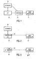
- Fig. 1 shows a data processing system comprising a microprocessor 10, a memory 15 belonging to the microprocessor, a controller 13 controlling the interaction between the system components and a video controller 17.
- This system may be situated in a reduced-power mode.
- the video controller 17 In the reduced-power mode it is important to make optimum use of the various system components. In the reduced-power mode the video controller 17 often reproduces a limited quantity of information. This requires a memory in which this information is stored. By utilizing the memory 15 belonging to the microprocessor 10, the use of a memory of its own of the video controller 17 can be avoided.
- the microprocessor 10 in the reduced mode is less active or inactive, which result in a reduced use of the memory 15.
- the capacity of the memory 15 that is vacated may be used by the video controller 17. If the microprocessor 10 is switched off in the reduced-power mode, the whole part of the memory 15 that is assigned to the microprocessor 10 becomes available to the video controller 17.
- the memory 15 will suffice as the sole memory for the video controller 17, because in the normal-power mode the video controller 17 does not need a memory and the memory 15 is thus again completely available to the microprocessor 10.
- Fig. 2 shows a data processing system comprising a microprocessor 20, a video controller 27, an external memory 25 belonging to the microprocessor, and a controller 23 included in the microprocessor 20.
- the controller 23 controls, possibly commanded by the microprocessor 20, the access to the memory 25 belonging to the microprocessor 20.
- the video controller 27 can utilize the memory 25 belonging to the microprocessor 20 in the reduced-power mode, the use of a memory of its own belonging to the video controller 27 can be avoided.
- the microprocessor 20 can be switched off, whereas the access to the memory 25 is maintained for the video controller 27.
- the energy consumption is reduced and the system components are made optimum use of.
- the memory 25 will suffice as the sole memory for the video controller 27, because the video controller 27 in the normal-power mode does not need any memory and the memory 25 is thus again completely at the disposal of the microprocessor 20.
- Fig. 3 shows a data processing system comprising a video controller 27, a microprocessor 30 including a memory 35 inside the microprocessor 30, which memory is accessible to the video controller 37 from the exterior in the reduced-power mode.
- the microprocessor 30 is not switched off in some systems, but needs to execute only a minimum set of tasks. To this end, the microprocessor 30 needs to have only a small portion of the memory 35, whereas yet the whole memory 35 is to be supplied with energy.
- the video controller 37 By allowing the video controller 37 to make use of the unused part of the memory 35, the use of an additional memory belonging to the video controller 37 can be avoided. As a result, also the energy consumption associated to the memory belonging to the video controller 17 is avoided and optimum use is made of the available system components.
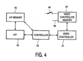
- Fig. 4 shows a data processing system comprising a microprocessor 40, a controller 43, a memory 45 belonging to the microprocessor, a video controller 47, a memory 49 belonging to the video controller 47, and a switch 48 for interrupting the energy supply to the memory 49.
- the controller 43 offers the video controller 47 access to the memory 45 belonging to the microprocessor 40.
- the memory 45 has sufficient storage capacity for the data of the video controller 47 in the reduced-power mode.
- the memory 49 belonging to the video controller 47 is no longer necessary in the reduced-power mode and can be switched off by a switch 49 or a power-down pin 46, so that there is a reduction of energy consumption.
- the switching-off of the memory 49 belonging to the video controller 47 may be combined with the improvements shown in Figs. 1, 2 and 3 .
Priority Applications (1)
| Application Number | Priority Date | Filing Date | Title |
|---|---|---|---|
| EP00974554.8A EP1157370B1 (en) | 1999-11-24 | 2000-11-15 | Data processing unit with access to the memory of another data processing unit during standby |
Applications Claiming Priority (4)
| Application Number | Priority Date | Filing Date | Title |
|---|---|---|---|
| EP99203936 | 1999-11-24 | ||
| EP99203936 | 1999-11-24 | ||
| PCT/EP2000/011428 WO2001039164A1 (en) | 1999-11-24 | 2000-11-15 | Data processing unit with access to the memory of another data processing unit during standby |
| EP00974554.8A EP1157370B1 (en) | 1999-11-24 | 2000-11-15 | Data processing unit with access to the memory of another data processing unit during standby |
Publications (2)
| Publication Number | Publication Date |
|---|---|
| EP1157370A1 EP1157370A1 (en) | 2001-11-28 |
| EP1157370B1 true EP1157370B1 (en) | 2014-09-03 |
Family
ID=8240902
Family Applications (1)
| Application Number | Title | Priority Date | Filing Date |
|---|---|---|---|
| EP00974554.8A Expired - Lifetime EP1157370B1 (en) | 1999-11-24 | 2000-11-15 | Data processing unit with access to the memory of another data processing unit during standby |
Country Status (6)
| Country | Link |
|---|---|
| US (1) | US6963987B1 (ja) |
| EP (1) | EP1157370B1 (ja) |
| JP (1) | JP2003515831A (ja) |
| KR (1) | KR100769557B1 (ja) |
| CN (1) | CN1188795C (ja) |
| WO (1) | WO2001039164A1 (ja) |
Families Citing this family (20)
| Publication number | Priority date | Publication date | Assignee | Title |
|---|---|---|---|---|
| US7230933B2 (en) * | 2002-04-17 | 2007-06-12 | Microsoft Corporation | Reducing idle power consumption in a networked battery operated device |
| JP4180834B2 (ja) | 2002-05-01 | 2008-11-12 | 富士通株式会社 | 情報処理装置および情報処理プログラム |
| JP2006502488A (ja) * | 2002-10-11 | 2006-01-19 | コーニンクレッカ フィリップス エレクトロニクス エヌ ヴィ | 省電力vliwプロセッサ |
| TWI242970B (en) * | 2004-04-02 | 2005-11-01 | Htc Corp | Frame refreshing method and handheld electronic device using the method |
| DE102005016830A1 (de) * | 2004-04-14 | 2005-11-03 | Denso Corp., Kariya | Halbleitervorrichtung und Verfahren zu ihrer Herstellung |
| EP1626328A1 (en) * | 2004-08-13 | 2006-02-15 | Dialog Semiconductor GmbH | Power saving during idle loop |
| EP1640966B1 (en) * | 2004-09-23 | 2012-09-19 | HTC Corporation | Frame refresh method and circuit |
| US7222253B2 (en) * | 2004-12-28 | 2007-05-22 | Intel Corporation | Dynamic power control for reducing voltage level of graphics controller component of memory controller based on its degree of idleness |
| US7373537B2 (en) * | 2005-06-28 | 2008-05-13 | Intel Corporation | Response to wake event while a system is in reduced power consumption state |
| EP1958071B1 (en) * | 2005-11-15 | 2012-03-07 | Oracle America, Inc. | Power conservation via dram access |
| US7873788B1 (en) | 2005-11-15 | 2011-01-18 | Oracle America, Inc. | Re-fetching cache memory having coherent re-fetching |
| CN101356510B (zh) * | 2005-11-15 | 2013-04-03 | 太阳微系统有限公司 | 当处理器处于低功率状态时可为后台dma装置提供数据的小型高功效高速缓冲存储器 |
| US7958312B2 (en) | 2005-11-15 | 2011-06-07 | Oracle America, Inc. | Small and power-efficient cache that can provide data for background DMA devices while the processor is in a low-power state |
| US7899990B2 (en) | 2005-11-15 | 2011-03-01 | Oracle America, Inc. | Power conservation via DRAM access |
| US7516274B2 (en) | 2005-11-15 | 2009-04-07 | Sun Microsystems, Inc. | Power conservation via DRAM access reduction |
| US7934054B1 (en) | 2005-11-15 | 2011-04-26 | Oracle America, Inc. | Re-fetching cache memory enabling alternative operational modes |
| US7536511B2 (en) * | 2006-07-07 | 2009-05-19 | Advanced Micro Devices, Inc. | CPU mode-based cache allocation for image data |
| KR101330121B1 (ko) * | 2006-10-30 | 2013-11-26 | 삼성전자주식회사 | 컴퓨터시스템 및 그 제어방법 |
| US8041848B2 (en) | 2008-08-04 | 2011-10-18 | Apple Inc. | Media processing method and device |
| US9128842B2 (en) * | 2012-09-28 | 2015-09-08 | Intel Corporation | Apparatus and method for reducing the flushing time of a cache |
Family Cites Families (24)
| Publication number | Priority date | Publication date | Assignee | Title |
|---|---|---|---|---|
| EP0405318A3 (en) * | 1989-06-20 | 1991-11-27 | Nec Corporation | Microprocessor having cash bypass signal terminal |
| GB2260631B (en) * | 1991-10-17 | 1995-06-28 | Intel Corp | Microprocessor 2X core design |
| US5450549A (en) * | 1992-04-09 | 1995-09-12 | International Business Machines Corporation | Multi-channel image array buffer and switching network |
| JPH06215160A (ja) * | 1992-08-25 | 1994-08-05 | Texas Instr Inc <Ti> | データ処理方法および装置 |
| US5638530A (en) * | 1993-04-20 | 1997-06-10 | Texas Instruments Incorporated | Direct memory access scheme using memory with an integrated processor having communication with external devices |
| WO1995015528A1 (en) * | 1993-11-30 | 1995-06-08 | Vlsi Technology, Inc. | A reallocatable memory subsystem enabling transparent transfer of memory function during upgrade |
| US5632038A (en) * | 1994-02-22 | 1997-05-20 | Dell Usa, L.P. | Secondary cache system for portable computer |
| FI100280B (fi) * | 1994-10-07 | 1997-10-31 | Nokia Mobile Phones Ltd | Menetelmä tehonkulutuksen minimoimiseksi tietokonelaitteessa |
| US5669003A (en) * | 1994-12-23 | 1997-09-16 | Intel Corporation | Method of monitoring system bus traffic by a CPU operating with reduced power |
| US5530932A (en) * | 1994-12-23 | 1996-06-25 | Intel Corporation | Cache coherent multiprocessing computer system with reduced power operating features |
| US5768628A (en) * | 1995-04-14 | 1998-06-16 | Nvidia Corporation | Method for providing high quality audio by storing wave tables in system memory and having a DMA controller on the sound card for transferring the wave tables |
| US5845139A (en) * | 1995-06-07 | 1998-12-01 | Advanced Micro Devices, Inc. | System for providing a host computer with access to a memory on a PCMCIA card in a power down mode |
| US5963721A (en) * | 1995-12-29 | 1999-10-05 | Texas Instruments Incorporated | Microprocessor system with capability for asynchronous bus transactions |
| US5907330A (en) * | 1996-12-18 | 1999-05-25 | Intel Corporation | Reducing power consumption and bus bandwidth requirements in cellular phones and PDAS by using a compressed display cache |
| EP0855718A1 (en) * | 1997-01-28 | 1998-07-29 | Hewlett-Packard Company | Memory low power mode control |
| US6185704B1 (en) * | 1997-04-11 | 2001-02-06 | Texas Instruments Incorporated | System signaling schemes for processor and memory module |
| US5941968A (en) * | 1997-04-14 | 1999-08-24 | Advanced Micro Devices, Inc. | Computer system for concurrent data transferring between graphic controller and unified system memory and between CPU and expansion bus device |
| US6052133A (en) | 1997-06-27 | 2000-04-18 | S3 Incorporated | Multi-function controller and method for a computer graphics display system |
| JPH11161385A (ja) * | 1997-11-28 | 1999-06-18 | Toshiba Corp | コンピュータシステムおよびそのシステムステート制御方法 |
| US6134609A (en) * | 1998-03-31 | 2000-10-17 | Micron Electronics, Inc. | Method for using computer system memory as a modem data buffer by transferring modem I/O data directly to system controller and transferring corresponding system controller data directly to main memory |
| US6105141A (en) * | 1998-06-04 | 2000-08-15 | Apple Computer, Inc. | Method and apparatus for power management of an external cache of a computer system |
| US6347294B1 (en) * | 1998-09-22 | 2002-02-12 | International Business Machines Corporation | Upgradeable highly integrated embedded CPU system |
| US6381636B1 (en) * | 1999-03-10 | 2002-04-30 | International Business Machines Corporation | Data processing system and method for permitting a server to remotely access a powered-off client computer system's asset information |
| US6523128B1 (en) * | 1999-08-31 | 2003-02-18 | Intel Corporation | Controlling power for a sleeping state of a computer to prevent overloading of the stand-by power rails by selectively asserting a control signal |
-
2000
- 2000-11-15 KR KR1020017009221A patent/KR100769557B1/ko not_active IP Right Cessation
- 2000-11-15 EP EP00974554.8A patent/EP1157370B1/en not_active Expired - Lifetime
- 2000-11-15 WO PCT/EP2000/011428 patent/WO2001039164A1/en active Application Filing
- 2000-11-15 CN CNB008053197A patent/CN1188795C/zh not_active Expired - Fee Related
- 2000-11-15 JP JP2001540752A patent/JP2003515831A/ja not_active Withdrawn
- 2000-11-21 US US09/717,966 patent/US6963987B1/en not_active Expired - Fee Related
Also Published As
| Publication number | Publication date |
|---|---|
| CN1188795C (zh) | 2005-02-09 |
| WO2001039164A1 (en) | 2001-05-31 |
| KR20020007294A (ko) | 2002-01-26 |
| JP2003515831A (ja) | 2003-05-07 |
| CN1344403A (zh) | 2002-04-10 |
| EP1157370A1 (en) | 2001-11-28 |
| US6963987B1 (en) | 2005-11-08 |
| KR100769557B1 (ko) | 2007-10-23 |
Similar Documents
| Publication | Publication Date | Title |
|---|---|---|
| EP1157370B1 (en) | Data processing unit with access to the memory of another data processing unit during standby | |
| US6360327B1 (en) | System with control registers for managing computer legacy peripheral devices using an advanced configuration power interface software power management system | |
| US6065124A (en) | Computer system having power saving and management function and method of controlling the same | |
| US5721934A (en) | Retrofit external power saving system and method for use | |
| US6591368B1 (en) | Method and apparatus for controlling power of computer system using wake up LAN (local area network) signal | |
| US5167024A (en) | Power management for a laptop computer with slow and sleep modes | |
| US6985755B2 (en) | Reduced power consumption wireless interface device | |
| US9015503B2 (en) | Power control methods for a portable electronic device | |
| US7574615B2 (en) | Method of managing power consumption of a network interface | |
| JP4463216B2 (ja) | 省電力機能を備えた無線通信端末 | |
| EP2188693B1 (en) | Apparatus and method for reducing power consumption in system on chip | |
| EP1306758A3 (en) | Computer system having resume function | |
| JP2006221381A (ja) | プロセッサシステム、該プロセッサシステムを備えた画像形成装置 | |
| US20080005461A1 (en) | Power-saving control apparatus, power-saving control method, and computer product | |
| CA2024552A1 (en) | Power management for a laptop computer | |
| KR20110038036A (ko) | 슬리프 프로세서 | |
| US5978924A (en) | Computer system with an advanced power saving function and an operating method therefor | |
| US5237698A (en) | Microcomputer | |
| JPH11221951A (ja) | 情報処理装置、モード制御方法及び記憶媒体 | |
| JP2003323236A (ja) | 情報処理装置および情報処理プログラム | |
| WO2005026928A2 (en) | Power saving operation of an apparatus with a cache memory | |
| US20020083357A1 (en) | Method and apparatus for lossless resume capability with peripheral devices | |
| JPH09251334A (ja) | 消費電力制御方式 | |
| JP2004021603A (ja) | 電子機器およびサスペンド/レジューム方法 | |
| US7321980B2 (en) | Software power control of circuit modules in a shared and distributed DMA system |
Legal Events
| Date | Code | Title | Description |
|---|---|---|---|
| PUAI | Public reference made under article 153(3) epc to a published international application that has entered the european phase |
Free format text: ORIGINAL CODE: 0009012 |
|
| AK | Designated contracting states |
Kind code of ref document: A1 Designated state(s): AT BE CH CY DE DK ES FI FR GB GR IE IT LI LU MC NL PT SE |
|
| 17P | Request for examination filed |
Effective date: 20011130 |
|
| RBV | Designated contracting states (corrected) |
Designated state(s): DE FR GB IT |
|
| RAP1 | Party data changed (applicant data changed or rights of an application transferred) |
Owner name: NXP B.V. |
|
| 17Q | First examination report despatched |
Effective date: 20071213 |
|
| RAP1 | Party data changed (applicant data changed or rights of an application transferred) |
Owner name: DSP GROUP SWITZERLAND AG |
|
| GRAP | Despatch of communication of intention to grant a patent |
Free format text: ORIGINAL CODE: EPIDOSNIGR1 |
|
| INTG | Intention to grant announced |
Effective date: 20140313 |
|
| GRAS | Grant fee paid |
Free format text: ORIGINAL CODE: EPIDOSNIGR3 |
|
| GRAA | (expected) grant |
Free format text: ORIGINAL CODE: 0009210 |
|
| AK | Designated contracting states |
Kind code of ref document: B1 Designated state(s): DE FR GB IT |
|
| REG | Reference to a national code |
Ref country code: GB Ref legal event code: FG4D |
|
| REG | Reference to a national code |
Ref country code: DE Ref legal event code: R096 Ref document number: 60048707 Country of ref document: DE Effective date: 20141016 |
|
| REG | Reference to a national code |
Ref country code: DE Ref legal event code: R097 Ref document number: 60048707 Country of ref document: DE |
|
| PLBE | No opposition filed within time limit |
Free format text: ORIGINAL CODE: 0009261 |
|
| STAA | Information on the status of an ep patent application or granted ep patent |
Free format text: STATUS: NO OPPOSITION FILED WITHIN TIME LIMIT |
|
| 26N | No opposition filed |
Effective date: 20150604 |
|
| GBPC | Gb: european patent ceased through non-payment of renewal fee |
Effective date: 20141203 |
|
| REG | Reference to a national code |
Ref country code: FR Ref legal event code: ST Effective date: 20150731 |
|
| PG25 | Lapsed in a contracting state [announced via postgrant information from national office to epo] |
Ref country code: IT Free format text: LAPSE BECAUSE OF FAILURE TO SUBMIT A TRANSLATION OF THE DESCRIPTION OR TO PAY THE FEE WITHIN THE PRESCRIBED TIME-LIMIT Effective date: 20140903 |
|
| PG25 | Lapsed in a contracting state [announced via postgrant information from national office to epo] |
Ref country code: GB Free format text: LAPSE BECAUSE OF NON-PAYMENT OF DUE FEES Effective date: 20141203 |
|
| PG25 | Lapsed in a contracting state [announced via postgrant information from national office to epo] |
Ref country code: FR Free format text: LAPSE BECAUSE OF NON-PAYMENT OF DUE FEES Effective date: 20141201 |
|
| PGFP | Annual fee paid to national office [announced via postgrant information from national office to epo] |
Ref country code: DE Payment date: 20151119 Year of fee payment: 16 |
|
| REG | Reference to a national code |
Ref country code: DE Ref legal event code: R119 Ref document number: 60048707 Country of ref document: DE |
|
| PG25 | Lapsed in a contracting state [announced via postgrant information from national office to epo] |
Ref country code: DE Free format text: LAPSE BECAUSE OF NON-PAYMENT OF DUE FEES Effective date: 20170601 |