EP1156584B1 - A method for shaping thin film resonators to shape acoustic modes therein - Google Patents
A method for shaping thin film resonators to shape acoustic modes therein Download PDFInfo
- Publication number
- EP1156584B1 EP1156584B1 EP01304145A EP01304145A EP1156584B1 EP 1156584 B1 EP1156584 B1 EP 1156584B1 EP 01304145 A EP01304145 A EP 01304145A EP 01304145 A EP01304145 A EP 01304145A EP 1156584 B1 EP1156584 B1 EP 1156584B1
- Authority
- EP
- European Patent Office
- Prior art keywords
- resonator
- shaped
- masking material
- acoustic resonator
- etching
- Prior art date
- Legal status (The legal status is an assumption and is not a legal conclusion. Google has not performed a legal analysis and makes no representation as to the accuracy of the status listed.)
- Expired - Lifetime
Links
- 238000000034 method Methods 0.000 title claims description 46
- 238000007493 shaping process Methods 0.000 title claims description 12
- 239000010409 thin film Substances 0.000 title claims description 10
- 239000000463 material Substances 0.000 claims description 63
- 238000005530 etching Methods 0.000 claims description 19
- 239000000758 substrate Substances 0.000 claims description 18
- 230000000873 masking effect Effects 0.000 claims description 14
- 238000001020 plasma etching Methods 0.000 claims description 10
- 239000000126 substance Substances 0.000 claims description 8
- 238000005498 polishing Methods 0.000 claims description 6
- 229920002120 photoresistant polymer Polymers 0.000 claims description 5
- 239000002904 solvent Substances 0.000 claims description 5
- 238000010438 heat treatment Methods 0.000 claims description 4
- 238000000206 photolithography Methods 0.000 claims description 4
- 238000007704 wet chemistry method Methods 0.000 claims description 4
- LLHKCFNBLRBOGN-UHFFFAOYSA-N propylene glycol methyl ether acetate Chemical group COCC(C)OC(C)=O LLHKCFNBLRBOGN-UHFFFAOYSA-N 0.000 claims description 3
- 230000002463 transducing effect Effects 0.000 claims description 3
- 238000010884 ion-beam technique Methods 0.000 claims description 2
- 238000000059 patterning Methods 0.000 claims 2
- 238000006073 displacement reaction Methods 0.000 claims 1
- 230000008569 process Effects 0.000 description 20
- 239000010408 film Substances 0.000 description 18
- VYPSYNLAJGMNEJ-UHFFFAOYSA-N Silicium dioxide Chemical compound O=[Si]=O VYPSYNLAJGMNEJ-UHFFFAOYSA-N 0.000 description 11
- XUIMIQQOPSSXEZ-UHFFFAOYSA-N Silicon Chemical compound [Si] XUIMIQQOPSSXEZ-UHFFFAOYSA-N 0.000 description 7
- 238000004519 manufacturing process Methods 0.000 description 7
- 229910052710 silicon Inorganic materials 0.000 description 7
- 239000010703 silicon Substances 0.000 description 7
- PMHQVHHXPFUNSP-UHFFFAOYSA-M copper(1+);methylsulfanylmethane;bromide Chemical compound Br[Cu].CSC PMHQVHHXPFUNSP-UHFFFAOYSA-M 0.000 description 6
- 230000033001 locomotion Effects 0.000 description 6
- 230000008859 change Effects 0.000 description 5
- 230000004044 response Effects 0.000 description 5
- 239000000377 silicon dioxide Substances 0.000 description 5
- 238000005229 chemical vapour deposition Methods 0.000 description 4
- 230000000694 effects Effects 0.000 description 4
- 150000002500 ions Chemical class 0.000 description 4
- 235000012239 silicon dioxide Nutrition 0.000 description 4
- 238000003491 array Methods 0.000 description 3
- 230000005684 electric field Effects 0.000 description 3
- 238000001914 filtration Methods 0.000 description 3
- 239000012528 membrane Substances 0.000 description 3
- 230000009467 reduction Effects 0.000 description 3
- PIGFYZPCRLYGLF-UHFFFAOYSA-N Aluminum nitride Chemical compound [Al]#N PIGFYZPCRLYGLF-UHFFFAOYSA-N 0.000 description 2
- KRHYYFGTRYWZRS-UHFFFAOYSA-N Fluorane Chemical compound F KRHYYFGTRYWZRS-UHFFFAOYSA-N 0.000 description 2
- XLOMVQKBTHCTTD-UHFFFAOYSA-N Zinc monoxide Chemical compound [Zn]=O XLOMVQKBTHCTTD-UHFFFAOYSA-N 0.000 description 2
- 230000000739 chaotic effect Effects 0.000 description 2
- 230000008878 coupling Effects 0.000 description 2
- 238000010168 coupling process Methods 0.000 description 2
- 238000005859 coupling reaction Methods 0.000 description 2
- 239000013078 crystal Substances 0.000 description 2
- 239000002178 crystalline material Substances 0.000 description 2
- 239000007789 gas Substances 0.000 description 2
- 230000010354 integration Effects 0.000 description 2
- ZBSCCQXBYNSKPV-UHFFFAOYSA-N oxolead;oxomagnesium;2,4,5-trioxa-1$l^{5},3$l^{5}-diniobabicyclo[1.1.1]pentane 1,3-dioxide Chemical compound [Mg]=O.[Pb]=O.[Pb]=O.[Pb]=O.O1[Nb]2(=O)O[Nb]1(=O)O2 ZBSCCQXBYNSKPV-UHFFFAOYSA-N 0.000 description 2
- 239000004065 semiconductor Substances 0.000 description 2
- 238000004544 sputter deposition Methods 0.000 description 2
- 230000002889 sympathetic effect Effects 0.000 description 2
- JBRZTFJDHDCESZ-UHFFFAOYSA-N AsGa Chemical compound [As]#[Ga] JBRZTFJDHDCESZ-UHFFFAOYSA-N 0.000 description 1
- LPOUEVYXAMBSRF-UHFFFAOYSA-N [Zr].[Ta].[Co].[Fe] Chemical compound [Zr].[Ta].[Co].[Fe] LPOUEVYXAMBSRF-UHFFFAOYSA-N 0.000 description 1
- 230000001944 accentuation Effects 0.000 description 1
- 229910045601 alloy Inorganic materials 0.000 description 1
- 239000000956 alloy Substances 0.000 description 1
- 229910052782 aluminium Inorganic materials 0.000 description 1
- XAGFODPZIPBFFR-UHFFFAOYSA-N aluminium Chemical compound [Al] XAGFODPZIPBFFR-UHFFFAOYSA-N 0.000 description 1
- 230000015556 catabolic process Effects 0.000 description 1
- 238000006243 chemical reaction Methods 0.000 description 1
- 239000011248 coating agent Substances 0.000 description 1
- 238000000576 coating method Methods 0.000 description 1
- 230000001427 coherent effect Effects 0.000 description 1
- 238000010276 construction Methods 0.000 description 1
- 238000006731 degradation reaction Methods 0.000 description 1
- 230000001066 destructive effect Effects 0.000 description 1
- 230000001627 detrimental effect Effects 0.000 description 1
- 238000005516 engineering process Methods 0.000 description 1
- 230000005284 excitation Effects 0.000 description 1
- 239000005357 flat glass Substances 0.000 description 1
- 230000003993 interaction Effects 0.000 description 1
- 238000001459 lithography Methods 0.000 description 1
- 230000008018 melting Effects 0.000 description 1
- 238000002844 melting Methods 0.000 description 1
- 238000003801 milling Methods 0.000 description 1
- 230000003287 optical effect Effects 0.000 description 1
- 239000013307 optical fiber Substances 0.000 description 1
- 238000002360 preparation method Methods 0.000 description 1
- 230000000644 propagated effect Effects 0.000 description 1
- 239000010453 quartz Substances 0.000 description 1
- 239000002002 slurry Substances 0.000 description 1
- 230000003595 spectral effect Effects 0.000 description 1
- 238000000427 thin-film deposition Methods 0.000 description 1
- 239000011787 zinc oxide Substances 0.000 description 1
Images


Classifications
-
- H—ELECTRICITY
- H03—ELECTRONIC CIRCUITRY
- H03H—IMPEDANCE NETWORKS, e.g. RESONANT CIRCUITS; RESONATORS
- H03H9/00—Networks comprising electromechanical or electro-acoustic elements; Electromechanical resonators
- H03H9/15—Constructional features of resonators consisting of piezoelectric or electrostrictive material
- H03H9/17—Constructional features of resonators consisting of piezoelectric or electrostrictive material having a single resonator
- H03H9/171—Constructional features of resonators consisting of piezoelectric or electrostrictive material having a single resonator implemented with thin-film techniques, i.e. of the film bulk acoustic resonator [FBAR] type
- H03H9/172—Means for mounting on a substrate, i.e. means constituting the material interface confining the waves to a volume
- H03H9/175—Acoustic mirrors
-
- H—ELECTRICITY
- H03—ELECTRONIC CIRCUITRY
- H03H—IMPEDANCE NETWORKS, e.g. RESONANT CIRCUITS; RESONATORS
- H03H3/00—Apparatus or processes specially adapted for the manufacture of impedance networks, resonating circuits, resonators
- H03H3/007—Apparatus or processes specially adapted for the manufacture of impedance networks, resonating circuits, resonators for the manufacture of electromechanical resonators or networks
- H03H3/02—Apparatus or processes specially adapted for the manufacture of impedance networks, resonating circuits, resonators for the manufacture of electromechanical resonators or networks for the manufacture of piezoelectric or electrostrictive resonators or networks
Definitions
- the present invention relates to the field ofradio frequency (RF) electrical filters, frequency control elements and oscillators having resonators and, more particularly, to a process for structuring a thin film resonator to advantageously shape the mode of the acoustic resonator such that the electrical and acoustic performance of the resonator are enhanced.
- RF radio frequency
- Thin film resonators are thin film acoustic devices which can resonate in the radio frequency to microwave range, for example, 0.5 to 5 Gigahertz (GHz), in response to an electrical signal.
- TFR's are often formed of piezoelectric elements. Piezoelectric elements are cleaved from a substrate according to a process described in US Patent 5 650 675 .
- a typical TFR has a piezoelectric film between a first electrode and a second electrode which apply an electric field to the piezoelectric film.
- the film is made of a piezoelectric crystalline material, such as zinc oxide, aluminum-nitride (AlN) or other piezoelectric crystalline material, which exhibits a piezoelectric effect.
- the piezoelectric effect occurs when the piezoelectric material expands or contracts in response to an electric field applied across the piezoelectric material, for example by the first and second electrodes, or produces charge or current in response to mechanical stress or strain applied to the piezoelectric material.
- the piezoelectric material will produce a maximum amount of current at this resonance frequency because of the mechanical motion which is large in magnitude.
- Piezoelectric film is useful as an element in electrical filters, oscillators, or frequency control circuits because it yields different amounts of current at different frequencies.
- the resonating or transducing material is magnetostrictive or electrostrictive (i.e., CoFeTaZr alloys (cobalt iron tantalum zirconium) or PMN (Lead Magnesium Niobate))
- electric filters can also be made using mechanical resonators because, as in piezoelectric material, an RF source will cause the resonating material to mechanically move.
- Boundaries at the upper and lower surfaces of a piezoelectric material may be imposed to reflect acoustic waves excited in the material such that a sympathetic vibration (i.e., resonance) occurs at a desired frequency.
- a material can be polished with two flat interfaces separated by just enough material (for example, half of a wavelength at the propagation velocity of sound through the material) such that the transit time of a wave back and forth in the material occurs at a desired period.
- Such resonators can be made from bulk piezoelectric crystals which are polished to the desired dimensions.
- there is a practical limit to the highest frequency achievable in this manner which frequency occurs when polishing reduces the material to thicknesses so small that the material cannot be handled easily.
- TFRs can be used at radio frequency (RF) because piezoelectric films can be made thin, for example at higher frequencies, such as 0.5-10 GHz, the piezoelectric film can be between 0.4 and 8 microns in thickness. Piezoelectric resonators needed for these higher frequency applications can be made by using techniques similar to those used to manufacture integrated circuits.
- the TFR structure can be formed on the substrate, such as a silicon (Si), Gallium Arsenide (GaAs) or other semiconductor substrate, for monolithic integration purposes, such as integration with active semiconductor devices. If the TFR has acoustic reflecting layer(s) as explained below, the acoustic reflecting layer(s) are formed on the substrate followed by the second electrode which is formed on the reflecting layer(s).
- the second electrode is formed on the substrate, for example using chemical vapor deposition (CVD) or sputtering. See, Kern & Vossen, Thin Film Processes, Vols. I and II, Wiley & Sons .
- the piezoelectric film is then formed on the second electrode, and the first electrode is formed on top of the piezoelectric film, for example using chemical vapor deposition (CVD) or sputtering.
- an acoustic mirror may be manufactured by repeatedly causing small reflections from many interfaces between different materials and ensuring all the reflections sum constructively. For example, in the resonator 10 shown in Fig.
- each mirror layer should have a thickness of exactly one quarter of the wave length of sound at the desired frequency.
- an AlN film will be typically 2.5 microns thick, and the electrodes may be 300 microns across for an optimum match to a 50 Ohm circuit.
- the ratio of the material thickness to lateral dimension is small, and the sound energy is not laterally well confined.
- Detrimental interactions between different types of acoustic waves (modes) and the edge of the resonator occur, and large fields at the edge of the resonator may create unwanted motions in the resonator. Any of these effects remove energy from the desired vibration and degrade resonator quality.
- the present invention is a process for lithographically shaping a resonator such that a predominance of acoustic energy is provided at desired locations within the resonator. For example, by providing a resonator which is shaped to be constructed thicker in its middle, the resonant mode shape becomes changed such that the resonant mode will also be greater at the middle of the resonator.
- the mode shape is seen when an instantaneous "snapshot" of a standing resonant wave is taken; it shows where a response amplitude of motion is large and where it is small.
- the fractional amount of energy which is converted to unwanted vibrations by the edge of the resonator is reduced.
- This resonator lithographic shaping process can be used during batch-fabrication (i.e., where multiple thin film resonators are manufactured on a continuous silicon substrate of thin-film resonators which are used in high frequency applications.)
- the shaping is achieved using photolithography.
- Photo-definable resists can be positioned over areas of the substrate that are not meant to be removed. The resist itself will be removed at a rate such that it may only protect the substrate beneath it until the resist is removed. Material removal or an etching process can be used to transfer a shaped pattern in a resist to a shaped pattern in the piezoelectric material being removed.
- the lithographic shaping process includes utilising one of a heating schedule and vapor cycle to shape a masking material into a predetermined physical structure (e.g. a done) and removing the underlying material using the predetermined physical structure as a mask such that material is removed from the resonator to shape the acoustic resonator such that the acoustic modes within the acoustic resonator are shaped.
- a predetermined physical structure e.g. a done
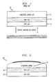
- Fig. 2 is an exemplary illustration of a domed piezo resonator 30 according to the present invention.
- the AlN 31 piezo layer
- layers of SiO 2 32, and AlN 33 are positioned beneath the domed layer of AlN 31 to act as an acoustic mirror.
- quartz crystals have mechanically polished domes and are also mechanically manufactured in order to perform improved filtering and frequency selection.
- the resonator 30 shown in Fig. 2 operates at high frequencies, where a fundamentally different preparation sequence is used.
- thin films are deposited on silicon (in a manner similar to that used when making computer chips) and all of the manufacturing steps are performed utilizing photo lithographic and etching techniques, such that a domed acoustic resonator 30 which advantageously guides the acoustic waves to the center of the resonator is obtained.
- the resonator In the resonator according to the present invention, if a sound wave is introduced into the resonator, the sound wave will enter, bounce off the opposing side and return to the point of origin. If the sound wave is entered into the resonator in phase, the sound wave will sum constructively with any sound wave which is already present. This is a simplified view of sympathetic vibration (i.e., resonance). Conversely, if the sound wave is entered into the resonator out of proper phase, the sound wave may destructively interfere with any sound wave which is already present.
- the time required for a sound wave to propagate, hit an opposite surface of a layer and return i.e., a reflection
- the sound wave propagates and reflects at an earlier time.
- Piezoelectric films are utilized for electronic filtering because their electrical properties exhibit useful characteristics at the mechanical resonance frequency of piezoelectric material. In such filters, the reduction of any signal degradation due to energy loss is vital.
- An example of loss in such a device is the creation of unwanted lateral excitations (drawing energy from the desired resonance mode) which is known to occur at the edge of the resonator. It is thus important to control the mode shapes in piezoelectric devices to enhance their electrical performance.
- the resonator can be shaped using techniques similar to those used in current microlens fabrication processes.
- the following patents provide examples of such micro lenses and microlens arrays.
- U.S. Patent No. 5,079,130 to Derkits, Jr. describes a refractive micro lenses process using photolithography and reactive ion etching.
- U.S. Patent No. 5,286,338 to Feldblum, et al. describes the production of diffractive micro-optic arrays using thin film deposition.
- U.S. Patent No. 5,011,254 to Edwards, et al. describes a process for manufacturing micro lenses directly on the end of optical fibers for coupling applications.
- U.S. Patent No. to 5,412,506 to Feldblum, et al. describes the fabrication of diffractive micro-optics using a multi-level etching process.
- Micro lenses are commercially available from companies such as Corning, Nippon Sheet Glass, and United Technologies.
- a lithographic method for making refractive micro lenses is disclosed in U.S. Patent No. 5,079,130 and is improved upon in U.S. Patent No. 5,286,338 .
- a cylindrical lenses may be made using the process described in U.S. Patent No. 5,286,338 . In this case, however, long rectangles (rather than cylinders) of resist are used.
- Diffractive microlens arrays are made by approximating an ideal diffractive optical surface profile with a series of planar levels; this produces a staircase effect. The more levels used, the greater the diffraction efficiency.
- An 8-level structure has a theoretical maximum diffraction efficiency of 95%, versus 99% for a 16-level structure. A series of lithographic exposures and reactive ion etching are used to fabricate these structures.
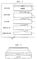
- FIG. 3 is an illustration of the process steps for producing a resonator 20 in accordance with the present invention.
- This process begins by coating a substrate 21 with photo resist 22 which is exposed and developed into "hockey-puck" cylinders 23.
- a photo resist is patterned into cylinders 23 and using a heating schedule (heat at 80° C, then 150° C for 10 minutes at each temperature, for example), the photo resist cylinders 23 are melted into dome shaped "drops 24."
- RIE reactive ion etching
- Partial resist 25 is obtained prior to completion of the RIE. Upon complete removal of the resist, removal of the substrate will also begin.
- etching process for example, reactive ion etching, wet chemistry or focus ion beam milling (FIB)
- the resist 25 and material 21 are then etched at the required rates (as set forth in the etching process) such that the final structure 26 possesses the desired amount of doming, contouring or shaping for guiding the acoustic waves to the center of the resonator.
- Reactive ion etching is the removal of material in a chamber into which reactive gases are introduced to chemically attack the surface to be removed.
- the removal process in FIB is enhanced by bombarding the surface of the material with high energy ions from an ionized plasma.
- CMP chemical mechanical polishing
- the initial pattern will be scaled as it is transferred to the underlying material.
- any step or dome height which existed in the resist will be doubled since the underlying material was etched at twice the etching rate of the resist.
- the type of material removal process used and the parameters of the process can be changed during the material removal stage to vary the relative etch rates of the resist and the underlying material such that the initial resist shape is tailored to a desired final shape. For example, change the type of reactive gas used during RIE, change the chemicals in which the wet etch is performed or change the type of chemicals used to perform the CMP. This provides greater flexibility during etching, and permits the creation of a broader range of final shapes.
- the photo resist 22 may be exposed to the vapors of a suitable resist solvent such as, for example, propylene glycol methyl ether acetate (PGMEA) to form the resist drops.
- a suitable resist solvent such as, for example, propylene glycol methyl ether acetate (PGMEA)
- PMEA propylene glycol methyl ether acetate
- the resist cylinders 23 are exposed to the vapors of the heated solvent in an evacuated heated chamber.
- the vapors of the solvent are absorbed by the resist cylinders 23, the temperature at which the material flows is lowered, and the resist cylinders 23 flow to form the resist layer 24.
- the use of vapor advantageously permits the use of much thinner resist layers. Resist thicknesses of 0.4 ⁇ m and greater can be used, as opposed to the several microns required using the melting technique. As a result, a substantial reduction in subsequent etching times is achieved.
- the resonator may be shaped such that it possesses low symmetry (when view from above).
- a circular resonator for example
- a non radially shaped resonator exhibits a lower level of constructive interference. Consequently, a resonator having a highly symmetric structure and a resonator having a low symmetric structure should be used to obtain a large constructive interference or a low constructive interference, respectively.
- lateral waves within the resonator it is desirable for lateral waves within the resonator to reflect in phase, and thus sum constructively.
- lateral waves may be fabricated at random phases (i.e., by constructing resonators having hatched scalloped, jagged or wavy edges, for example). This may prove advantageous in that it is possible to cause the sound waves to interfere in a non uniform manner, and thus reduce constructive interference.
- dishing instead of doming for applications where thicker boundary regions produce a mode with pronounced vibration at the resonator's edge.
- multiple domes within a resonator, or radial patterns may be preferred. Wash-boarding with multiple high and low rows may be employed according to an aspect which is not part of the invention.
- the shaping may be performed on any part of the device: the substrate, reflecting layers, piezoelectric resonator or the metallic electrodes. As a result of the shaping, the lateral motion of acoustic waves within the resonator may be controlled. This permits accentuation of the acoustic energy or the sound wave at desired locations within the resonator. This advantageously affects the performance of the resonator when used as a frequency selective device such as an oscillator or filter.
- the geometry of the resonator may be changed.
- the energy of the sound wave will be concentrated in the middle of the dome at certain frequencies due to the sound wave being propagated and reflected at the correct time such that the energy is constructively summed.
- the energy is less than optimally summed at identical frequencies because the wavelength is less than 1 ⁇ 2 lambda.
- a greater amount of energy is concentrated at the center of the resonator as a result of the less than optimal summing of the energy at the edges of the resonator.
- the foregoing is a simplified view of resonance phenomena of complicated geometries, but illustrates that energy can be concentrated in certain parts of a resonator depending on its construction and the frequency of operation.
- multiple layers of resist can be provided such that multiple etchings are performed to produce a resonator having a stepped shaping.
- Fig. 4 is an etchings are performed to produce a resonator having a stepped shaping.
- Fig. 4 is an illustration of a step-wise shape piezo resonator according to the present invention.
- Fig. 7 is a cross sectional illustration of a doubly step-wise shaped piezo electric resonator.
- the step-wise shaped piezo resonator shown in Fig. 4 includes silicon dioxide layers and aluminum nitride layers which acts as an acoustic mirror.
- the step-wise shaped piezo resonator may also split the mode into a multiplicity of modes to thereby add desired spectral features to the electrical response of the resonator.
- the doubly step-wise shaped resonator shown in Fig. 7 may also be constructed as a free standing membrane.
- the top layer of the acoustic mirror or a second electrode of the resonator may be constructed in a trenched manner such that the interface between the resonator and mirror is lowered at desired locations.
- resonators such that various shapes are achieved, for example a plano-convex shaped resonator (as shown in Fig. 5 ), or a doubly convex shaped resonator (as shown in Fig. 6 ). It is also possible to utilize the etching processes to shape the resonators such that they possess the combined features of the various resonators (see for example, Figs. 8 and 9 ). In addition to shaping resonators on mirrors, it is also desirable to shape freestanding membrane resonators and utilize them in broader band filtering applications.
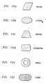
- Figs. 10(a) through 10(f) show top views of other contemplated embodiments of the present invention.
- These lower symmetry embodiments are shaped via photolithography or etching such that they focus sound waves in a manner which is advantageous for a particular application (i.e., repositioning the location of sound waves within resonators, for example).
- a conventional circular shaped resonator laterally moving sound waves propagate and reflect symmetrically.
- these waves can arrive in the middle of the resonator at the same time (in phase).
- the lower symmetry shaped resonators according to the invention do not cause the sound waves to propagate and reflect to the middle of the resonator in phase.
- the lower symmetry shaped resonators may cause the sound waves to reflect in a chaotic manner (random) or cause large amplitude vibrations at locations away from the resonator's center. As a result, an advantageous repositioning of the lateral propagation of the wave is achieved.
- the mode shape imposed by the embodiments shown in Figs. 10(a) through 10(f) changes as the operating frequency of the resonator is changed, due to coupling between the direction of the waves in the resonator and the nonparallel edges of the resonator. This change in mode shape can result in a desired frequency dependant change in the impedance of the resonator.
- the polygonal and trapezoidal embodiments shown in Figs. 10(a) and (c) possess mode shapes which are generally consistent with the symmetry of the resonator boundaries.
- the ellipsoidal embodiment shown in Fig.10(b) possesses a mode shape which comprises interposed ellipses and hyperbolas.
- the annulus embodiment shown in Fig. 10(e) possess a circular radial mode shape which is interposed with a sinusoidal angular pattern.
- the stadium embodiment shown in Fig. 10(f) possesses a chaotic shape.
- Resonators having the different edge configurations shown in Figs. 11(a) through 11(c) can be constructed and used to cause lateral waves within the resonator to reflect at random phases. This may prove advantageous in that it is possible to cause the sound waves to interfere in a non uniform manner, and thus reduce constructive interference (i.e., reduce reflection coherency). This reduction in reflection coherency occurs in a manner which is analogous to "roughing" the walls of a room to reduce unwanted coherent reflections.
Landscapes
- Physics & Mathematics (AREA)
- Acoustics & Sound (AREA)
- Engineering & Computer Science (AREA)
- Manufacturing & Machinery (AREA)
- Piezo-Electric Or Mechanical Vibrators, Or Delay Or Filter Circuits (AREA)
Applications Claiming Priority (2)
| Application Number | Priority Date | Filing Date | Title |
|---|---|---|---|
| US571919 | 2000-05-16 | ||
| US09/571,919 US6420202B1 (en) | 2000-05-16 | 2000-05-16 | Method for shaping thin film resonators to shape acoustic modes therein |
Publications (2)
| Publication Number | Publication Date |
|---|---|
| EP1156584A1 EP1156584A1 (en) | 2001-11-21 |
| EP1156584B1 true EP1156584B1 (en) | 2012-12-26 |
Family
ID=24285591
Family Applications (1)
| Application Number | Title | Priority Date | Filing Date |
|---|---|---|---|
| EP01304145A Expired - Lifetime EP1156584B1 (en) | 2000-05-16 | 2001-05-08 | A method for shaping thin film resonators to shape acoustic modes therein |
Country Status (3)
| Country | Link |
|---|---|
| US (1) | US6420202B1 (enExample) |
| EP (1) | EP1156584B1 (enExample) |
| JP (1) | JP5142001B2 (enExample) |
Families Citing this family (33)
| Publication number | Priority date | Publication date | Assignee | Title |
|---|---|---|---|---|
| CN1280025C (zh) * | 2001-06-01 | 2006-10-18 | 利特斯公司 | 微沉积系统以及在衬底上沉积精确量的流体材料的方法 |
| DE10135872A1 (de) * | 2001-07-24 | 2003-02-27 | Osram Opto Semiconductors Gmbh | Verfahren zur Herstellung einer Linse |
| US20030048041A1 (en) * | 2001-09-07 | 2003-03-13 | Hiroyuki Kita | Piezoelectric thin-film element and a manufacturing method thereof |
| JP3969224B2 (ja) * | 2002-01-08 | 2007-09-05 | 株式会社村田製作所 | 圧電共振子及びそれを用いた圧電フィルタ・デュプレクサ・通信装置 |
| US20100107389A1 (en) * | 2002-01-11 | 2010-05-06 | Avago Technologies Wireless Ip (Singapore) Pte. Ltd. | Method of fabricating an electrode for a bulk acoustic resonator |
| DE10200741A1 (de) * | 2002-01-11 | 2003-07-24 | Infineon Technologies Ag | Verfahren zur Herstellung einer topologieoptimierten Elektrode für einen Resonator in Dünnfilmtechnologie |
| US20040173144A1 (en) * | 2002-05-31 | 2004-09-09 | Edwards Charles O. | Formation of printed circuit board structures using piezo microdeposition |
| JP3829861B2 (ja) | 2002-08-07 | 2006-10-04 | 松下電器産業株式会社 | 角速度センサ |
| EP1540819A1 (en) * | 2002-09-12 | 2005-06-15 | Philips Intellectual Property & Standards GmbH | Bulk acoustic waver resonator with means for suppression of pass-band ripple in bulk acoustic wave filters |
| JP2004304704A (ja) * | 2003-04-01 | 2004-10-28 | Matsushita Electric Ind Co Ltd | 薄膜音響共振子、及び、薄膜音響共振子回路 |
| JP4133580B2 (ja) * | 2003-05-21 | 2008-08-13 | 独立行政法人科学技術振興機構 | 圧電材料の加工方法 |
| JP4012156B2 (ja) * | 2004-02-02 | 2007-11-21 | 独立行政法人科学技術振興機構 | 圧電素子の製造方法 |
| JP4149416B2 (ja) * | 2004-05-31 | 2008-09-10 | 富士通メディアデバイス株式会社 | 圧電薄膜共振子およびフィルタならびにそれらの製造方法 |
| JP2006140370A (ja) * | 2004-11-15 | 2006-06-01 | Oki Electric Ind Co Ltd | マイクロレンズの製造方法 |
| US7541893B2 (en) * | 2005-05-23 | 2009-06-02 | Cts Corporation | Ceramic RF filter and duplexer having improved third harmonic response |
| EP1887688A4 (en) * | 2005-06-02 | 2009-08-05 | Murata Manufacturing Co | PIEZOELECTRIC RESONATOR AND PIEZOELECTRIC THIN-FILTER FILTER |
| US7889027B2 (en) * | 2005-09-09 | 2011-02-15 | Sony Corporation | Film bulk acoustic resonator shaped as an ellipse with a part cut off |
| US7544612B1 (en) | 2006-01-20 | 2009-06-09 | Skyworks Solutions, Inc. | Method and structure for reducing the effect of vertical steps in patterned layers in semiconductor structures |
| US7598827B2 (en) | 2006-06-19 | 2009-10-06 | Maxim Integrated Products | Harmonic termination of power amplifiers using BAW filter output matching circuits |
| US7586389B2 (en) * | 2006-06-19 | 2009-09-08 | Maxim Integrated Products, Inc. | Impedance transformation and filter using bulk acoustic wave technology |
| JP2008078717A (ja) * | 2006-09-19 | 2008-04-03 | Nec Tokin Corp | ノイズフィルタおよびスイッチング電源 |
| US7385334B1 (en) | 2006-11-20 | 2008-06-10 | Sandia Corporation | Contour mode resonators with acoustic reflectors |
| DE112008002181B4 (de) * | 2007-08-14 | 2023-08-03 | Avago Technologies International Sales Pte. Limited | Bulkakustikwellenstruktur mit einer piezoelektrischen Aluminiumkupfernitrid-Schicht und darauf bezogenes Verfahren |
| WO2009023100A2 (en) * | 2007-08-14 | 2009-02-19 | Skyworks Solutions, Inc. | Method for forming a multi-layer electrode underlying a piezoelectric layer and related structure |
| US7777596B2 (en) * | 2007-12-18 | 2010-08-17 | Robert Bosch Gmbh | MEMS resonator structure and method |
| US7602102B1 (en) | 2008-04-24 | 2009-10-13 | Skyworks Solutions, Inc. | Bulk acoustic wave resonator with controlled thickness region having controlled electromechanical coupling |
| US7795781B2 (en) * | 2008-04-24 | 2010-09-14 | Avago Technologies Wireless Ip (Singapore) Pte. Ltd. | Bulk acoustic wave resonator with reduced energy loss |
| US7889025B1 (en) * | 2008-06-10 | 2011-02-15 | The United States Of America As Represented By The Secretary Of The Army | Anti-reflective acoustic diffuser for SAW and BAW devices |
| JP5288920B2 (ja) * | 2008-07-16 | 2013-09-11 | 日本電波工業株式会社 | 水晶振動用素子の製造方法 |
| CN101477194B (zh) * | 2009-02-17 | 2011-07-06 | 东南大学 | 一种转子碰摩声发射源定位方法 |
| US9608589B2 (en) | 2010-10-26 | 2017-03-28 | Avago Technologies General Ip (Singapore) Pte. Ltd. | Method of forming acoustic resonator using intervening seed layer |
| US10763823B2 (en) | 2015-12-30 | 2020-09-01 | 3M Innovative Properties Company | Elliptically-shaped resonator markers with enhanced frequency stability and gain |
| EP3863176B1 (en) * | 2018-10-23 | 2022-12-07 | Huawei Technologies Co., Ltd. | Method for preparing monolithic integrated baw resonator |
Family Cites Families (22)
| Publication number | Priority date | Publication date | Assignee | Title |
|---|---|---|---|---|
| JPS52658B2 (enExample) * | 1971-12-30 | 1977-01-10 | ||
| JPS58137317A (ja) * | 1982-02-09 | 1983-08-15 | Nec Corp | 圧電薄膜複合振動子 |
| US4556812A (en) * | 1983-10-13 | 1985-12-03 | The United States Of America As Represented By The United States Department Of Energy | Acoustic resonator with Al electrodes on an AlN layer and using a GaAs substrate |
| US4719383A (en) * | 1985-05-20 | 1988-01-12 | The United States Of America As Represented By The United States Department Of Energy | Piezoelectric shear wave resonator and method of making same |
| JP2644855B2 (ja) * | 1988-10-24 | 1997-08-25 | 株式会社日立製作所 | 弾性波フィルタ、及びそれを用いたアンテナ分波器 |
| US4966446A (en) | 1989-04-28 | 1990-10-30 | At&T Bell Laboratories | Mask controlled coupling of inter-substrate optical components |
| US4966447A (en) | 1989-04-28 | 1990-10-30 | At&T Bell Laboratories | Integration of free-space planar optical components |
| US5074646A (en) | 1989-04-28 | 1991-12-24 | At&T Bell Laboratories | Planar reflective optical devices |
| US5011254A (en) | 1989-11-30 | 1991-04-30 | At&T Bell Laboratories | Coupling of optical devices to optical fibers by means of microlenses |
| US5079130A (en) | 1990-05-25 | 1992-01-07 | At&T Bell Laboratories | Partially or fully recessed microlens fabrication |
| US5075641A (en) * | 1990-12-04 | 1991-12-24 | Iowa State University Research Foundation, Inc. | High frequency oscillator comprising cointegrated thin film resonator and active device |
| JP3362860B2 (ja) * | 1991-01-09 | 2003-01-07 | 大日本印刷株式会社 | 表面弾性波素子の製造方法 |
| JPH04322508A (ja) * | 1991-04-22 | 1992-11-12 | Matsushita Electric Ind Co Ltd | 水晶振動子の製造方法 |
| US5348617A (en) * | 1991-12-23 | 1994-09-20 | Iowa State University Research Foundation, Inc. | Selective etching process |
| US5412506A (en) | 1992-03-09 | 1995-05-02 | At&T Corp. | Free-space optical interconnection arrangement |
| US5286338A (en) | 1993-03-01 | 1994-02-15 | At&T Bell Laboratories | Methods for making microlens arrays |
| US5650075A (en) * | 1995-05-30 | 1997-07-22 | Motorola, Inc. | Method for etching photolithographically produced quartz crystal blanks for singulation |
| US5696423A (en) * | 1995-06-29 | 1997-12-09 | Motorola, Inc. | Temperature compenated resonator and method |
| US5918354A (en) * | 1996-04-02 | 1999-07-06 | Seiko Epson Corporation | Method of making a piezoelectric element |
| JPH10107573A (ja) * | 1996-09-30 | 1998-04-24 | Kyocera Corp | 弾性表面波装置 |
| JP2000040931A (ja) * | 1998-07-23 | 2000-02-08 | Matsushita Electric Ind Co Ltd | 圧電共振子、圧電共振子の製造方法および圧電共振子の周波数調整方法 |
| JP4036544B2 (ja) * | 1998-09-22 | 2008-01-23 | Tdk株式会社 | 電圧制御発振器 |
-
2000
- 2000-05-16 US US09/571,919 patent/US6420202B1/en not_active Expired - Lifetime
-
2001
- 2001-05-08 EP EP01304145A patent/EP1156584B1/en not_active Expired - Lifetime
- 2001-05-15 JP JP2001145259A patent/JP5142001B2/ja not_active Expired - Fee Related
Also Published As
| Publication number | Publication date |
|---|---|
| US6420202B1 (en) | 2002-07-16 |
| JP5142001B2 (ja) | 2013-02-13 |
| US20020022292A1 (en) | 2002-02-21 |
| JP2002043879A (ja) | 2002-02-08 |
| EP1156584A1 (en) | 2001-11-21 |
Similar Documents
| Publication | Publication Date | Title |
|---|---|---|
| EP1156584B1 (en) | A method for shaping thin film resonators to shape acoustic modes therein | |
| US7939356B2 (en) | Method of manufacturing film bulk acoustic resonator using internal stress of metallic film and resonator manufactured thereby | |
| EP0797300B1 (en) | Piezoelectric vibrator and manufacturing method thereof | |
| US8357981B2 (en) | Transducer devices having different frequencies based on layer thicknesses and method of fabricating the same | |
| US9015914B2 (en) | Method for manufacturing electronic component | |
| US6534900B2 (en) | Piezoresonator | |
| KR100662865B1 (ko) | 박막 벌크 음향 공진기 및 그 제조방법 | |
| JP2007181185A (ja) | 音響共振器およびその製造方法 | |
| CN112953446B (zh) | 一种体声波谐振器的制备方法以及体声波谐振器 | |
| KR20130044905A (ko) | 박막 벌크 음향 공진기 및 박막 벌크 음향 공진기의 제조방법 | |
| KR100745428B1 (ko) | 음향 공진 장치 및 그 제조 방법과 격리 방법 | |
| US20110115338A1 (en) | Methods of Fabricating a Membrane With Improved Mechanical Integrity | |
| JP2004328739A (ja) | 基板からフローティングされたエアギャップを有する薄膜のバルク音響共振器及びその製造方法 | |
| EP1742355A1 (en) | Piezoelectric thin film vibrator | |
| US7109637B2 (en) | Thin-film bulk acoustic oscillator and method of manufacturing same | |
| KR20220127125A (ko) | 에어갭형 fbar | |
| US8896188B2 (en) | Resonator electrodes and related methods and apparatus | |
| CN119543870B (zh) | 一种具有声传输结构的薄膜体声波谐振器 | |
| JPS6352486B2 (enExample) | ||
| CN117997304A (zh) | 一种谐振器及其制备方法 | |
| KR100857935B1 (ko) | 음향 미러의 제조 방법 및 압전 공명기의 제조 방법 | |
| CN119093891A (zh) | 边缘结构和滤波器 | |
| JPS6294010A (ja) | 圧電薄膜共振子の製造方法 | |
| KR20020029882A (ko) | 엘시엠피 공정법에 의한 탄성파소자의 제작방법 | |
| KR20040037906A (ko) | 압전체를 이용한 공진기 및 그 제조 방법 |
Legal Events
| Date | Code | Title | Description |
|---|---|---|---|
| PUAI | Public reference made under article 153(3) epc to a published international application that has entered the european phase |
Free format text: ORIGINAL CODE: 0009012 |
|
| AK | Designated contracting states |
Kind code of ref document: A1 Designated state(s): AT BE CH CY DE DK ES FI FR GB GR IE IT LI LU MC NL PT SE TR Kind code of ref document: A1 Designated state(s): DE FR GB |
|
| AX | Request for extension of the european patent |
Free format text: AL;LT;LV;MK;RO;SI |
|
| 17P | Request for examination filed |
Effective date: 20020128 |
|
| AKX | Designation fees paid |
Free format text: DE FR GB |
|
| 17Q | First examination report despatched |
Effective date: 20061208 |
|
| APBN | Date of receipt of notice of appeal recorded |
Free format text: ORIGINAL CODE: EPIDOSNNOA2E |
|
| APBR | Date of receipt of statement of grounds of appeal recorded |
Free format text: ORIGINAL CODE: EPIDOSNNOA3E |
|
| APAF | Appeal reference modified |
Free format text: ORIGINAL CODE: EPIDOSCREFNE |
|
| APBT | Appeal procedure closed |
Free format text: ORIGINAL CODE: EPIDOSNNOA9E |
|
| GRAC | Information related to communication of intention to grant a patent modified |
Free format text: ORIGINAL CODE: EPIDOSCIGR1 |
|
| GRAP | Despatch of communication of intention to grant a patent |
Free format text: ORIGINAL CODE: EPIDOSNIGR1 |
|
| GRAS | Grant fee paid |
Free format text: ORIGINAL CODE: EPIDOSNIGR3 |
|
| GRAA | (expected) grant |
Free format text: ORIGINAL CODE: 0009210 |
|
| AK | Designated contracting states |
Kind code of ref document: B1 Designated state(s): DE FR GB |
|
| REG | Reference to a national code |
Ref country code: GB Ref legal event code: FG4D |
|
| REG | Reference to a national code |
Ref country code: DE Ref legal event code: R081 Ref document number: 60147519 Country of ref document: DE Owner name: AVAGO TECHNOLOGIES GENERAL IP (SINGAPORE) PTE., SG Free format text: FORMER OWNER: AGERE SYSTEMS GUARDIAN CORP., ORLANDO, FLA., US |
|
| REG | Reference to a national code |
Ref country code: DE Ref legal event code: R096 Ref document number: 60147519 Country of ref document: DE Effective date: 20130228 |
|
| PLBE | No opposition filed within time limit |
Free format text: ORIGINAL CODE: 0009261 |
|
| STAA | Information on the status of an ep patent application or granted ep patent |
Free format text: STATUS: NO OPPOSITION FILED WITHIN TIME LIMIT |
|
| 26N | No opposition filed |
Effective date: 20130927 |
|
| REG | Reference to a national code |
Ref country code: DE Ref legal event code: R097 Ref document number: 60147519 Country of ref document: DE Effective date: 20130927 |
|
| REG | Reference to a national code |
Ref country code: DE Ref legal event code: R082 Ref document number: 60147519 Country of ref document: DE Representative=s name: DILG HAEUSLER SCHINDELMANN PATENTANWALTSGESELL, DE |
|
| PGFP | Annual fee paid to national office [announced via postgrant information from national office to epo] |
Ref country code: GB Payment date: 20140507 Year of fee payment: 14 |
|
| PGFP | Annual fee paid to national office [announced via postgrant information from national office to epo] |
Ref country code: FR Payment date: 20140509 Year of fee payment: 14 |
|
| GBPC | Gb: european patent ceased through non-payment of renewal fee |
Effective date: 20150508 |
|
| REG | Reference to a national code |
Ref country code: DE Ref legal event code: R082 Ref document number: 60147519 Country of ref document: DE Representative=s name: DILG HAEUSLER SCHINDELMANN PATENTANWALTSGESELL, DE Ref country code: DE Ref legal event code: R081 Ref document number: 60147519 Country of ref document: DE Owner name: AVAGO TECHNOLOGIES GENERAL IP (SINGAPORE) PTE., SG Free format text: FORMER OWNER: AGERE SYSTEMS GUARDIAN CORP., ORLANDO, FLA., US Ref country code: DE Ref legal event code: R081 Ref document number: 60147519 Country of ref document: DE Owner name: AVAGO TECHNOLOGIES INTERNATIONAL SALES PTE. LT, SG Free format text: FORMER OWNER: AGERE SYSTEMS GUARDIAN CORP., ORLANDO, FLA., US |
|
| REG | Reference to a national code |
Ref country code: FR Ref legal event code: ST Effective date: 20160129 |
|
| PG25 | Lapsed in a contracting state [announced via postgrant information from national office to epo] |
Ref country code: GB Free format text: LAPSE BECAUSE OF NON-PAYMENT OF DUE FEES Effective date: 20150508 |
|
| PG25 | Lapsed in a contracting state [announced via postgrant information from national office to epo] |
Ref country code: FR Free format text: LAPSE BECAUSE OF NON-PAYMENT OF DUE FEES Effective date: 20150601 |
|
| PGFP | Annual fee paid to national office [announced via postgrant information from national office to epo] |
Ref country code: DE Payment date: 20180419 Year of fee payment: 18 |
|
| REG | Reference to a national code |
Ref country code: DE Ref legal event code: R081 Ref document number: 60147519 Country of ref document: DE Owner name: AVAGO TECHNOLOGIES INTERNATIONAL SALES PTE. LT, SG Free format text: FORMER OWNER: AVAGO TECHNOLOGIES GENERAL IP (SINGAPORE) PTE. LTD., SINGAPORE, SG Ref country code: DE Ref legal event code: R082 Ref document number: 60147519 Country of ref document: DE Representative=s name: DILG HAEUSLER SCHINDELMANN PATENTANWALTSGESELL, DE |
|
| REG | Reference to a national code |
Ref country code: DE Ref legal event code: R119 Ref document number: 60147519 Country of ref document: DE |
|
| PG25 | Lapsed in a contracting state [announced via postgrant information from national office to epo] |
Ref country code: DE Free format text: LAPSE BECAUSE OF NON-PAYMENT OF DUE FEES Effective date: 20191203 |