EP1154468A2 - Method of depositing an amorphous carbon layer - Google Patents
Method of depositing an amorphous carbon layer Download PDFInfo
- Publication number
- EP1154468A2 EP1154468A2 EP01102401A EP01102401A EP1154468A2 EP 1154468 A2 EP1154468 A2 EP 1154468A2 EP 01102401 A EP01102401 A EP 01102401A EP 01102401 A EP01102401 A EP 01102401A EP 1154468 A2 EP1154468 A2 EP 1154468A2
- Authority
- EP
- European Patent Office
- Prior art keywords
- amorphous carbon
- layer
- substrate
- pattern
- carbon layer
- Prior art date
- Legal status (The legal status is an assumption and is not a legal conclusion. Google has not performed a legal analysis and makes no representation as to the accuracy of the status listed.)
- Granted
Links
Images



Classifications
-
- H—ELECTRICITY
- H10—SEMICONDUCTOR DEVICES; ELECTRIC SOLID-STATE DEVICES NOT OTHERWISE PROVIDED FOR
- H10P—GENERIC PROCESSES OR APPARATUS FOR THE MANUFACTURE OR TREATMENT OF DEVICES COVERED BY CLASS H10
- H10P14/00—Formation of materials, e.g. in the shape of layers or pillars
- H10P14/60—Formation of materials, e.g. in the shape of layers or pillars of insulating materials
- H10P14/69—Inorganic materials
- H10P14/6902—Inorganic materials composed of carbon, e.g. alpha-C, diamond or hydrogen doped carbon
-
- C—CHEMISTRY; METALLURGY
- C23—COATING METALLIC MATERIAL; COATING MATERIAL WITH METALLIC MATERIAL; CHEMICAL SURFACE TREATMENT; DIFFUSION TREATMENT OF METALLIC MATERIAL; COATING BY VACUUM EVAPORATION, BY SPUTTERING, BY ION IMPLANTATION OR BY CHEMICAL VAPOUR DEPOSITION, IN GENERAL; INHIBITING CORROSION OF METALLIC MATERIAL OR INCRUSTATION IN GENERAL
- C23C—COATING METALLIC MATERIAL; COATING MATERIAL WITH METALLIC MATERIAL; SURFACE TREATMENT OF METALLIC MATERIAL BY DIFFUSION INTO THE SURFACE, BY CHEMICAL CONVERSION OR SUBSTITUTION; COATING BY VACUUM EVAPORATION, BY SPUTTERING, BY ION IMPLANTATION OR BY CHEMICAL VAPOUR DEPOSITION, IN GENERAL
- C23C16/00—Chemical coating by decomposition of gaseous compounds, without leaving reaction products of surface material in the coating, i.e. chemical vapour deposition [CVD] processes
- C23C16/22—Chemical coating by decomposition of gaseous compounds, without leaving reaction products of surface material in the coating, i.e. chemical vapour deposition [CVD] processes characterised by the deposition of inorganic material, other than metallic material
- C23C16/26—Deposition of carbon only
-
- H—ELECTRICITY
- H10—SEMICONDUCTOR DEVICES; ELECTRIC SOLID-STATE DEVICES NOT OTHERWISE PROVIDED FOR
- H10P—GENERIC PROCESSES OR APPARATUS FOR THE MANUFACTURE OR TREATMENT OF DEVICES COVERED BY CLASS H10
- H10P14/00—Formation of materials, e.g. in the shape of layers or pillars
- H10P14/60—Formation of materials, e.g. in the shape of layers or pillars of insulating materials
- H10P14/66—Formation of materials, e.g. in the shape of layers or pillars of insulating materials characterised by the type of materials
- H10P14/662—Laminate layers, e.g. stacks of alternating high-k metal oxides
-
- H—ELECTRICITY
- H10—SEMICONDUCTOR DEVICES; ELECTRIC SOLID-STATE DEVICES NOT OTHERWISE PROVIDED FOR
- H10P—GENERIC PROCESSES OR APPARATUS FOR THE MANUFACTURE OR TREATMENT OF DEVICES COVERED BY CLASS H10
- H10P14/00—Formation of materials, e.g. in the shape of layers or pillars
- H10P14/60—Formation of materials, e.g. in the shape of layers or pillars of insulating materials
- H10P14/66—Formation of materials, e.g. in the shape of layers or pillars of insulating materials characterised by the type of materials
- H10P14/668—Formation of materials, e.g. in the shape of layers or pillars of insulating materials characterised by the type of materials the materials being characterised by the deposition precursor materials
-
- H—ELECTRICITY
- H10—SEMICONDUCTOR DEVICES; ELECTRIC SOLID-STATE DEVICES NOT OTHERWISE PROVIDED FOR
- H10P—GENERIC PROCESSES OR APPARATUS FOR THE MANUFACTURE OR TREATMENT OF DEVICES COVERED BY CLASS H10
- H10P50/00—Etching of wafers, substrates or parts of devices
- H10P50/20—Dry etching; Plasma etching; Reactive-ion etching
- H10P50/26—Dry etching; Plasma etching; Reactive-ion etching of conductive or resistive materials
- H10P50/264—Dry etching; Plasma etching; Reactive-ion etching of conductive or resistive materials by chemical means
- H10P50/266—Dry etching; Plasma etching; Reactive-ion etching of conductive or resistive materials by chemical means by vapour etching only
- H10P50/267—Dry etching; Plasma etching; Reactive-ion etching of conductive or resistive materials by chemical means by vapour etching only using plasmas
- H10P50/268—Dry etching; Plasma etching; Reactive-ion etching of conductive or resistive materials by chemical means by vapour etching only using plasmas of silicon-containing layers
-
- H—ELECTRICITY
- H10—SEMICONDUCTOR DEVICES; ELECTRIC SOLID-STATE DEVICES NOT OTHERWISE PROVIDED FOR
- H10P—GENERIC PROCESSES OR APPARATUS FOR THE MANUFACTURE OR TREATMENT OF DEVICES COVERED BY CLASS H10
- H10P50/00—Etching of wafers, substrates or parts of devices
- H10P50/20—Dry etching; Plasma etching; Reactive-ion etching
- H10P50/28—Dry etching; Plasma etching; Reactive-ion etching of insulating materials
- H10P50/286—Dry etching; Plasma etching; Reactive-ion etching of insulating materials of organic materials
- H10P50/287—Dry etching; Plasma etching; Reactive-ion etching of insulating materials of organic materials by chemical means
-
- H—ELECTRICITY
- H10—SEMICONDUCTOR DEVICES; ELECTRIC SOLID-STATE DEVICES NOT OTHERWISE PROVIDED FOR
- H10P—GENERIC PROCESSES OR APPARATUS FOR THE MANUFACTURE OR TREATMENT OF DEVICES COVERED BY CLASS H10
- H10P50/00—Etching of wafers, substrates or parts of devices
- H10P50/69—Etching of wafers, substrates or parts of devices using masks for semiconductor materials
- H10P50/691—Etching of wafers, substrates or parts of devices using masks for semiconductor materials for Group V materials or Group III-V materials
- H10P50/692—Etching of wafers, substrates or parts of devices using masks for semiconductor materials for Group V materials or Group III-V materials characterised by their composition, e.g. multilayer masks or materials
-
- H—ELECTRICITY
- H10—SEMICONDUCTOR DEVICES; ELECTRIC SOLID-STATE DEVICES NOT OTHERWISE PROVIDED FOR
- H10P—GENERIC PROCESSES OR APPARATUS FOR THE MANUFACTURE OR TREATMENT OF DEVICES COVERED BY CLASS H10
- H10P50/00—Etching of wafers, substrates or parts of devices
- H10P50/69—Etching of wafers, substrates or parts of devices using masks for semiconductor materials
- H10P50/691—Etching of wafers, substrates or parts of devices using masks for semiconductor materials for Group V materials or Group III-V materials
- H10P50/693—Etching of wafers, substrates or parts of devices using masks for semiconductor materials for Group V materials or Group III-V materials characterised by their size, orientation, disposition, behaviour or shape, in horizontal or vertical plane
- H10P50/696—Process specially adapted to improve the resolution of the mask
-
- H—ELECTRICITY
- H10—SEMICONDUCTOR DEVICES; ELECTRIC SOLID-STATE DEVICES NOT OTHERWISE PROVIDED FOR
- H10P—GENERIC PROCESSES OR APPARATUS FOR THE MANUFACTURE OR TREATMENT OF DEVICES COVERED BY CLASS H10
- H10P50/00—Etching of wafers, substrates or parts of devices
- H10P50/73—Etching of wafers, substrates or parts of devices using masks for insulating materials
-
- H—ELECTRICITY
- H10—SEMICONDUCTOR DEVICES; ELECTRIC SOLID-STATE DEVICES NOT OTHERWISE PROVIDED FOR
- H10P—GENERIC PROCESSES OR APPARATUS FOR THE MANUFACTURE OR TREATMENT OF DEVICES COVERED BY CLASS H10
- H10P76/00—Manufacture or treatment of masks on semiconductor bodies, e.g. by lithography or photolithography
- H10P76/20—Manufacture or treatment of masks on semiconductor bodies, e.g. by lithography or photolithography of masks comprising organic materials
- H10P76/204—Manufacture or treatment of masks on semiconductor bodies, e.g. by lithography or photolithography of masks comprising organic materials of organic photoresist masks
- H10P76/2041—Photolithographic processes
- H10P76/2043—Photolithographic processes using an anti-reflective coating
-
- H—ELECTRICITY
- H10—SEMICONDUCTOR DEVICES; ELECTRIC SOLID-STATE DEVICES NOT OTHERWISE PROVIDED FOR
- H10W—GENERIC PACKAGES, INTERCONNECTIONS, CONNECTORS OR OTHER CONSTRUCTIONAL DETAILS OF DEVICES COVERED BY CLASS H10
- H10W20/00—Interconnections in chips, wafers or substrates
- H10W20/01—Manufacture or treatment
- H10W20/071—Manufacture or treatment of dielectric parts thereof
- H10W20/074—Manufacture or treatment of dielectric parts thereof of dielectric parts comprising thin functional dielectric layers, e.g. dielectric etch-stop, barrier, capping or liner layers
-
- H—ELECTRICITY
- H10—SEMICONDUCTOR DEVICES; ELECTRIC SOLID-STATE DEVICES NOT OTHERWISE PROVIDED FOR
- H10W—GENERIC PACKAGES, INTERCONNECTIONS, CONNECTORS OR OTHER CONSTRUCTIONAL DETAILS OF DEVICES COVERED BY CLASS H10
- H10W20/00—Interconnections in chips, wafers or substrates
- H10W20/01—Manufacture or treatment
- H10W20/071—Manufacture or treatment of dielectric parts thereof
- H10W20/081—Manufacture or treatment of dielectric parts thereof by forming openings in the dielectric parts
-
- H—ELECTRICITY
- H10—SEMICONDUCTOR DEVICES; ELECTRIC SOLID-STATE DEVICES NOT OTHERWISE PROVIDED FOR
- H10W—GENERIC PACKAGES, INTERCONNECTIONS, CONNECTORS OR OTHER CONSTRUCTIONAL DETAILS OF DEVICES COVERED BY CLASS H10
- H10W20/00—Interconnections in chips, wafers or substrates
- H10W20/01—Manufacture or treatment
- H10W20/071—Manufacture or treatment of dielectric parts thereof
- H10W20/081—Manufacture or treatment of dielectric parts thereof by forming openings in the dielectric parts
- H10W20/084—Manufacture or treatment of dielectric parts thereof by forming openings in the dielectric parts for dual-damascene structures
-
- H—ELECTRICITY
- H10—SEMICONDUCTOR DEVICES; ELECTRIC SOLID-STATE DEVICES NOT OTHERWISE PROVIDED FOR
- H10D—INORGANIC ELECTRIC SEMICONDUCTOR DEVICES
- H10D64/00—Electrodes of devices having potential barriers
- H10D64/01—Manufacture or treatment
- H10D64/013—Manufacture or treatment of electrodes having a conductor capacitively coupled to a semiconductor by an insulator
- H10D64/01302—Manufacture or treatment of electrodes having a conductor capacitively coupled to a semiconductor by an insulator the insulator being formed after the semiconductor body, the semiconductor being silicon
- H10D64/01304—Manufacture or treatment of electrodes having a conductor capacitively coupled to a semiconductor by an insulator the insulator being formed after the semiconductor body, the semiconductor being silicon characterised by the conductor
- H10D64/01306—Manufacture or treatment of electrodes having a conductor capacitively coupled to a semiconductor by an insulator the insulator being formed after the semiconductor body, the semiconductor being silicon characterised by the conductor the conductor comprising a layer of silicon contacting the insulator, e.g. polysilicon
-
- H—ELECTRICITY
- H10—SEMICONDUCTOR DEVICES; ELECTRIC SOLID-STATE DEVICES NOT OTHERWISE PROVIDED FOR
- H10P—GENERIC PROCESSES OR APPARATUS FOR THE MANUFACTURE OR TREATMENT OF DEVICES COVERED BY CLASS H10
- H10P14/00—Formation of materials, e.g. in the shape of layers or pillars
- H10P14/60—Formation of materials, e.g. in the shape of layers or pillars of insulating materials
- H10P14/63—Formation of materials, e.g. in the shape of layers or pillars of insulating materials characterised by the formation processes
- H10P14/6326—Deposition processes
- H10P14/6328—Deposition from the gas or vapour phase
- H10P14/6334—Deposition from the gas or vapour phase using decomposition or reaction of gaseous or vapour phase compounds, i.e. chemical vapour deposition
- H10P14/6336—Deposition from the gas or vapour phase using decomposition or reaction of gaseous or vapour phase compounds, i.e. chemical vapour deposition in the presence of a plasma [PECVD]
-
- H—ELECTRICITY
- H10—SEMICONDUCTOR DEVICES; ELECTRIC SOLID-STATE DEVICES NOT OTHERWISE PROVIDED FOR
- H10P—GENERIC PROCESSES OR APPARATUS FOR THE MANUFACTURE OR TREATMENT OF DEVICES COVERED BY CLASS H10
- H10P14/00—Formation of materials, e.g. in the shape of layers or pillars
- H10P14/60—Formation of materials, e.g. in the shape of layers or pillars of insulating materials
- H10P14/69—Inorganic materials
- H10P14/6903—Inorganic materials containing silicon
- H10P14/6905—Inorganic materials containing silicon being a silicon carbide or silicon carbonitride and not containing oxygen, e.g. SiC or SiC:H
-
- H—ELECTRICITY
- H10—SEMICONDUCTOR DEVICES; ELECTRIC SOLID-STATE DEVICES NOT OTHERWISE PROVIDED FOR
- H10P—GENERIC PROCESSES OR APPARATUS FOR THE MANUFACTURE OR TREATMENT OF DEVICES COVERED BY CLASS H10
- H10P14/00—Formation of materials, e.g. in the shape of layers or pillars
- H10P14/60—Formation of materials, e.g. in the shape of layers or pillars of insulating materials
- H10P14/69—Inorganic materials
- H10P14/692—Inorganic materials composed of oxides, glassy oxides or oxide-based glasses
- H10P14/6921—Inorganic materials composed of oxides, glassy oxides or oxide-based glasses containing silicon
- H10P14/6922—Inorganic materials composed of oxides, glassy oxides or oxide-based glasses containing silicon the material containing Si, O and at least one of H, N, C, F or other non-metal elements, e.g. SiOC, SiOC:H or SiONC
Definitions
- the present invention relates to an amorphous carbon film, its use in integrated circuit fabrication, and a method for depositing the film.
- Integrated circuits have evolved into complex devices that can include millions of transistors, capacitors and resistors on a single chip.
- the evolution of chip designs continually requires faster circuitry and greater circuit density.
- the demands for faster circuits with greater circuit densities impose corresponding demands on the materials used to fabricate such integrated circuits.
- low resistivity conductive materials e. g., copper
- low dielectric constant insulating materials dielectric constant less than about 4.5
- a layer of energy sensitive resist is formed over a stack of material layers on a substrate.
- An image of a pattern is introduced into the energy sensitive resist layer.
- the pattern introduced into the energy sensitive resist layer is transferred into one or more layers of the material stack formed on the substrate using the layer of energy sensitive resist as a mask.
- the pattern introduced into the energy sensitive resist can be transferred into one or more layers of the material stack using a chemical etchant.
- the chemical etchant is designed to have a greater etch selectivity for the material layers of the stack than for the energy sensitive resist.
- the chemical etchant etches the one or more layers of the material stack at a much faster rate than it etches the energy sensitive resist.
- the faster etch rate for the one or more material layers of the stack typically prevents the energy sensitive resist material from being consumed prior to completion of the pattern transfer.
- An intermediate oxide layer e.g., silicon dioxide, silicon nitride
- a hardmask is often used between the energy sensitive resist layer and the underlying material layers to facilitate pattern transfer into the underlying material layers.
- some material structures e.g., damascene
- silicon dioxide and/or silicon nitride layers Such material structures cannot be patterned using a silicon dioxide or silicon nitride hardmask as an etch mask.
- Resist patterning problems are further compounded when lithographic imaging tools having deep ultraviolet (DUV) imaging wavelengths (e. g., less than about 250 nanometers (nm)) are used to generate the resist patterns.
- DUV imaging wavelengths improve resist pattern resolution because diffraction effects are reduced at these shorter wavelengths.
- the increased reflective nature of many underlying materials e. g., polysilicon and metal silicides
- ARC anti-reflective coating
- ARC materials have been suggested for use in combination with energy sensitive resists.
- U. S. Patent 5,626,967 issued May 6, 1997 to Pramanick et al. describes the use of titanium nitride anti-reflective coatings.
- titanium nitride is increasingly metallic as the exposure wavelength is reduced below 248 nm, meaning titanium nitride has high reflectivity for DUV radiation and is not an effective anti-reflective coating for DUV wavelengths.
- the present invention provides a method for forming an amorphous carbon layer for use in integrated circuit fabrication.
- the amorphous carbon layer is formed by thermally decomposing a gas mixture comprising a hydrocarbon compound and an inert gas.
- the gas mixture which may optionally include an additive gas, is introduced into a process chamber where plasma enhanced thermal decomposition of the hydrocarbon compound in close proximity to a substrate surface, results in deposition of an amorphous carbon layer on the substrate surface.
- An as-deposited amorphous carbon layer deposited according to the process of the invention, has an adjustable carbon:hydrogen ratio that ranges from about 10 % hydrogen to about 60 % hydrogen.
- the amorphous carbon layer also has a light absorption coefficient, k, that can be varied between about 0.1 to about 1.0 at wavelengths below about 250 nm, making it suitable for use as an anti-reflective coating (ARC) at DUV wavelengths.
- ARC anti-reflective coating
- the amorphous carbon layer is compatible with integrated circuit fabrication processes.
- the amorphous carbon layer is used as a hardmask.
- a preferred process sequence includes depositing an amorphous carbon layer on a substrate. After the amorphous carbon layer is deposited on the substrate, an intermediate layer is formed thereon. A pattern is defined in the intermediate layer and transferred into the amorphous carbon layer. Thereafter, the pattern is transferred into the substrate using the amorphous carbon layer as a hardmask. Additionally, the pattern defined in the amorphous carbon hardmask can be incorporated into the structure of the integrated circuit, such as for example in a damascene structure.
- the amorphous carbon layer is used as a single layer anti-reflective coating for DUV lithography.
- a preferred process sequence includes forming the amorphous carbon layer on a substrate.
- the amorphous carbon layer has a refractive index (n) in the range of about 1.5 to 1.9 and an absorption coefficient (k) in the range of about 0.1 to about 1.0 at wavelengths less than about 250 nm.
- the refractive index (n) and absorption coefficient (k) for the amorphous carbon ARC are tunable, in that they can be varied in the desired range as a function of the temperature and composition of the gas mixture during layer formation.
- a layer of energy sensitive resist material is formed thereon.
- a pattern is defined in the energy sensitive resist at a wavelength less than about 250 nm. Thereafter, the pattern defined in the energy sensitive resist is transferred into the amorphous carbon layer. After the amorphous carbon layer is patterned, such pattern is optionally transferred into the substrate.
- a multi-layer amorphous carbon anti-reflective coating is used for DUV lithography.
- a preferred process sequence includes forming a first amorphous carbon layer on a substrate.
- the first amorphous carbon layer has an index of refraction in the range of about 1.5 to about 1.9 and an absorption coefficient (k) in the range of about 0.5 to about 1.0 at wavelengths less than about 250 nm.
- k absorption coefficient
- a second amorphous carbon layer is formed thereon.
- the second amorphous carbon layer has an index of refraction of about 1.5 to about 1.9 and an absorption coefficient in the range of about 0.1 to about 0.5.
- the refractive index (n) and absorption coefficient (k) for the first and second amorphous carbon layers are tunable, in that they can be varied in the desired range as a function of the temperature and composition of the gas mixture during layer formation.
- a layer of energy sensitive resist material is formed on the second amorphous carbon layer.
- a pattern is defined in the energy sensitive resist layer at a wavelength less than about 250 nm. The pattern defined in the energy sensitive resist material is thereafter transferred into the second amorphous carbon layer followed by the first amorphous carbon layer. After the first amorphous carbon layer is patterned, such pattern is optionally transferred into the substrate.
- An aspect of the invention is a method of forming an amorphous carbon layer on a substrate comprising positioning a substrate in a deposition chamber; providing a gas mixture to the deposition chamber, wherein the gas mixture comprises one or more hydrocarbon compounds and an inert gas; and heating the gas mixture to thermally decompose the one or more hydrocarbon compounds in the gas mixture to form an amorphous carbon layer on the substrate.
- a preferred aspect of the above invention is a method wherein the amorphous carbon layer has an index of refraction in the range of about 1.5 to about 1.9.
- a preferred aspect of the above invention is a method wherein the amorphous carbon layer has an absorption coefficient in the range of about 0.1 to about 1.0, at wavelengths less than about 250 nm.
- An aspect of the invention is a method of forming a device, comprising forming one or more amorphous carbon layers on a substrate; and defining a pattern in at least one region of the one or more amorphous carbon layers.
- a preferred aspect of the above invention is a method further comprising transferring the pattern defined in the at least one region of the one or more amorphous carbon layers into the substrate using the one or more amorphous carbon layers as a mask.
- a preferred aspect of the above invention is a method further comprising the step of removing the one or more amorphous carbon layers from the substrate.
- a preferred aspect of the above invention is a method wherein the substrate has one or more material layers formed thereon.
- a preferred aspect of the above invention is a method wherein the oxide is selected from the group consisting of silicon dioxide, silicon nitride, silicon oxynitride, silicon carbide, and amorphous silicon.
- a preferred aspect of the above invention is a method wherein the one or more amorphous carbon layers are removed from the substrate using an ozone, oxygen, or NH 3 plasma.
- a preferred aspect of the above invention is a method wherein the one or more amorphous carbon layers each have an index of refraction in the range of about 1.5 to about 1.9.
- a preferred aspect of the above invention is a method wherein the one or more amorphous carbon layers are formed on the substrate by positioning the substrate in a deposition chamber; providing a gas mixture to the deposition chamber, wherein the gas mixture comprises one or more hydrocarbon compounds and an inert gas; and heating the gas mixture to thermally decompose the one or more hydrocarbon compounds in the gas mixture to form the one or more amorphous carbon layers on the substrate.
- a preferred aspect of the above invention is a method wherein the one or more amorphous carbon layers each have a thickness in the range of about 50 ⁇ to about 1500 ⁇ .
- a preferred aspect of the above invention is a method wherein the patterned radiation has a wavelength less than about 250 nanometers (nm).
- An aspect of the invention is a method of fabricating a damascene structure, comprising forming a dielectric layer on a substrate; forming an amorphous carbon layer on the dielectric layer; patterning the amorphous carbon layer to define contacts/vias therethrough; transferring the pattern formed in the amorphous carbon layer through the dielectric layer to form contacts/vias therein; removing the amorphous carbon layer from the patterned dielectric layer; and filling the contacts/vias formed in the dielectric layer with a conductive material.
- a preferred aspect of the above invention is a method wherein the dielectric layer has a dielectric constant less than about 4.5.
- a preferred aspect of the above invention is a method wherein the conductive material filling the contacts/vias has a resistivity less than about 5 ⁇ -cm.
- a preferred aspect of the above invention is a method wherein the dielectric layer is selected from the group consisting of silicon dioxide and fluorosilicate glass.
- a preferred aspect of the above invention is a method wherein the conductive material filling the contacts/vias is selected from the group consisting of copper, aluminum, tungsten, and combinations thereof.
- a preferred aspect of the above invention is a method wherein the one or more hydrocarbon compounds is selected from the group consisting of propylene (C 3 H 6 ), propyne (C 3 H 4 ), propane (C 3 H 8 ), butane (C 4 H 10 ), butylene (C 4 H 8 ), butadiene (C 4 H 6 ), or acetelyne (C 2 H 2 ) and combinations thereof.
- the one or more hydrocarbon compounds is selected from the group consisting of propylene (C 3 H 6 ), propyne (C 3 H 4 ), propane (C 3 H 8 ), butane (C 4 H 10 ), butylene (C 4 H 8 ), butadiene (C 4 H 6 ), or acetelyne (C 2 H 2 ) and combinations thereof.
- a preferred aspect of the above invention is a method wherein the amorphous carbon layer has a carbon:hydrogen ratio in the range of about 10 % hydrogen to about 60 % hydrogen.
- a preferred aspect of the above invention is a method wherein the inert gas is selected from the group consisting of helium, argon and combinations thereof.
- a preferred aspect of the above invention is a method wherein the gas mixture further comprises an additive gas.
- a preferred aspect of the above invention is a method wherein the additive gas is selected from the group consisting of ammonia, nitrogen, hydrogen, and combinations thereof.
- a preferred aspect of the above invention is a method wherein the substrate is heated to a temperature between about 100 °C and about 500 °C.
- a preferred aspect of the above invention is a method wherein the deposition chamber is maintained at a pressure between about 1 Torr to about 20 Torr.
- a preferred aspect of the above invention is a method wherein the gas mixture is provided to the deposition chamber at a flow rate in a range of about 50 sccm to about 500 sccm.
- a preferred aspect of the above invention is a method wherein the electric field applied to the gas mixture is a radio frequency (RF) power.
- RF radio frequency
- a preferred aspect of the above invention is a method wherein the amorphous carbon layer has a thickness in the range of about 200 ⁇ to about 1000 ⁇ .
- An aspect of the invention is a computer storage medium containing a software routine that, when executed, causes a general purpose computer to control a deposition chamber according to any of the above methods.
- the present invention provides a method of forming an integrated circuit using an amorphous carbon layer.
- the amorphous carbon layer is formed by thermally decomposing a gas mixture comprising a hydrocarbon compound and an inert gas.
- the gas mixture which may optionally include an additive gas, is introduced into a process chamber where plasma enhanced thermal decomposition of the hydrocarbon compound in close proximity to a substrate surface, results in deposition of an amorphous carbon layer on the substrate surface.
- the amorphous carbon layer is compatible with integrated circuit fabrication processes, discussed below.
- FIG. 1 is a schematic representation of a wafer processing system 10 that can be used to perform amorphous carbon layer deposition in accordance with the present invention.
- This apparatus typically comprises a process chamber 100, a gas panel 130, a control unit 110, along with other hardware components such as power supplies and vacuum pumps. Details of the system 10 used in the present invention are described in a commonly assigned U.S. patent application, entitled “High Temperature Chemical Vapor Deposition Chamber", Serial No. 09/211,998, filed on December 14, 1998, and is herein incorporated by reference. The salient features of this system 10 are briefly described below. Examples of system 10 include CENTURA® systems, PRECISION 5000® systems and PRODUCERTM systems commercially available from Applied Materials Inc., Santa Clara, California.
- the process chamber 100 generally comprises a support pedestal 150, which is used to support a substrate such as a semiconductor wafer 190.
- This pedestal 150 can typically be moved in a vertical direction inside the chamber 100 using a displacement mechanism (not shown).
- the wafer 190 can be heated to some desired temperature prior to processing.
- the wafer support pedestal 150 is heated by an embedded heater element 170.
- the pedestal 150 may be resistively heated by applying an electric current from an AC supply 106 to the heater element 170.
- the wafer 190 is, in turn, heated by the pedestal 150.
- a temperature sensor 172 such as a thermocouple, is also embedded in the wafer support pedestal 150 to monitor the temperature of the pedestal 150 in a conventional manner.
- the measured temperature is used in a feedback loop to control the power supply 16 for the heating element 170 such that the wafer temperature can be maintained or controlled at a desired temperature which is suitable for the particular process application.
- the pedestal 150 is optionally heated using a plasma or by radiant heat (not shown).
- a vacuum pump 102 is used to evacuate the process chamber 100 and to maintain the proper gas flows and pressure inside the chamber 100.
- a showerhead 120 through which process gases are introduced into the chamber 100, is located above the wafer support pedestal 150.
- the showerhead 120 is connected to a gas panel 130, which controls and supplies various gases used in different steps of the process sequence.
- the showerhead 120 and wafer support pedestal 150 also form a pair of spaced apart electrodes. When an electric field is generated between these electrodes, the process gases introduced into the chamber 100 are ignited into a plasma. Typically, the electric field is generated by connecting the wafer support pedestal 150 to a source of radio frequency (RF) power (not shown) through a matching network (not shown). Alternatively, the RF power source and matching network may be coupled to the showerhead 120, or coupled to both the showerhead 120 and the wafer support pedestal 150.
- RF radio frequency
- Plasma enhanced chemical vapor deposition (PECVD) techniques promote excitation and/or disassociation of the reactant gases by the application of the electric field to the reaction zone near the substrate surface, creating a plasma of reactive species.
- the reactivity of the species in the plasma reduces the energy required for a chemical reaction to take place, in effect lowering the required temperature for such PECVD processes.
- amorphous carbon layer deposition is accomplished by plasma enhanced thermal decomposition of a hydrocarbon compound such as propylene (C 3 H 6 ).
- a hydrocarbon compound such as propylene (C 3 H 6 ).
- Propylene is introduced into the process chamber 100 under the control of gas panel 130.
- the hydrocarbon compound is introduced into the process chamber as a gas with a regulated flow.
- the control unit 110 comprises a central processing unit (CPU) 112, support circuitry 114, and memories containing associated control software 116.
- This control unit 110 is responsible for automated control of the numerous steps required for wafer processing - such as wafer transport, gas flow control, temperature control, chamber evacuation, and so on. Bi-directional communications between the control unit 110 and the various components of the apparatus 10 are handled through numerous signal cables collectively referred to as signal buses 118, some of which are illustrated in FIG. 1.
- the heated pedestal 150 used in the present invention is made of aluminum, and comprises a heating element 170 embedded at a distance below the wafer support surface 151 of the pedestal 150.
- the heating element 170 can be made of a nickel-chromium wire encapsulated in an Incoloy sheath tube.
- the wafer 190 and the pedestal 150 can be maintained at a relatively constant temperature during film deposition. This is accomplished by a feedback control loop, in which the temperature of the pedestal 150 is continuously monitored by a thermocouple 172 embedded in the pedestal 150. This information is transmitted to the control unit 110 via a signal bus 118, which responds by sending the necessary signals to the heater power supply.
- Adjustment is subsequently made in the current supply 106 so as to maintain and control the pedestal 150 at a desirable temperature - i.e., a temperature that is appropriate for the specific process application.
- a desirable temperature i.e., a temperature that is appropriate for the specific process application.
- the amorphous carbon layer is formed from a gas mixture of a hydrocarbon compound and an inert gas such as argon (Ar) or helium (He).
- the hydrocarbon compound has a general formula C x H y , where x has a range of between 2 and 4 and y has a range of between 2 and 10.
- propylene (C 3 H 6 ), propyne (C 3 H 4 ), propane (C 3 H 8 ), butane (C 4 H 10 ), butylene (C 4 H 8 ), butadiene (C 4 H 6 ), or acetelyne (C 2 H 2 ) as well as combinations thereof, may be used as the hydrocarbon compound.
- gases such as hydrogen (H 2 ), nitrogen (N 2 ), ammonia (NH 3 ), or combinations thereof, among others, may be added to the gas mixture, if desired.
- Ar, He, and N 2 are used to control the density and deposition rate of the amorphous carbon layer.
- the addition of H 2 and/or NH 3 can be used to control the hydrogen ratio of the amorphous carbon layer, as discussed below.
- the following deposition process parameters can be used to form the amorphous carbon layer.
- the process parameters range from a wafer temperature of about 100°C to about 500°C, a chamber pressure of about 1 torr to about 20 torr, a hydrocarbon gas (C x H y ) flow rate of about 50 seem to about 500 seem (per 8 inch wafer), a RF power of between about 3 W/in 2 to about 20 W/in 2 , and a plate spacing of between about 300 mils to about 600 mils.
- the above process parameters provide a typical deposition rate for the amorphous carbon layer in the range of about 100 ⁇ /min to about 1000 ⁇ /min and can be implemented on a 200 mm substrate in a deposition chamber available from Applied Materials, Inc.
- deposition chambers are within the scope of the invention and the parameters listed above may vary according to the particular deposition chamber used to form the amorphous carbon layer.
- other deposition chambers may have a larger or smaller volume, requiring gas flow rates that are larger or smaller than those recited for deposition chambers available from Applied Materials, Inc.
- the as-deposited amorphous carbon layer has an adjustable carbon:hydrogen ratio that ranges from about 10 % hydrogen to about 60 % hydrogen. Controlling the hydrogen ratio of the amorphous carbon layer is desirable for tuning its optical properties as well as its etch selectivity. Specifically, as the hydrogen ratio decreases the optical properties of the as-deposited layer such as for example, the index of refraction (n) and the absorption coefficient (k) increase. Similarly, as the hydrogen ratio decreases the etch resistance of the amorphous carbon layer increases.
- the light absorption coefficient, k, of the amorphous carbon layer can be varied between about 0.1 to about 1.0 at wavelengths below about 250 nm, making it suitable for use as an anti-reflective coating (ARC) at DUV wavelengths.
- the absorption coefficient of the amorphous carbon layer can be varied as a function of the deposition temperature. In particular, as the temperature increases the absorption coefficient of the as-deposited layer likewise increases. For example, when propylene is the hydrocarbon compound the k value for the as-deposited amorphous carbon layers can be increased from about 0.2 to about 0.7 by increasing the deposition temperature from about 150 °C to about 480 °C.
- the absorption coefficient of the amorphous carbon layer can also be varied as a function of the additive used in the gas mixture.
- the presence of H 2 , NH 3 , N 2 or combinations thereof, in the gas mixture can increase the k value by about 10 % to about 100 %.
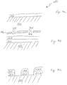
- FIGS. 2a-e illustrate schematic cross-sectional views of a substrate 200 at different stages of an integrated circuit fabrication sequence incorporating an amorphous carbon layer as a hardmask.
- the substrate 200 refers to any workpiece on which processing is performed, and a substrate structure 250 is used to generally denote the substrate 200 together with other material layers formed on the substrate 200.
- the substrate 200 may correspond to a silicon substrate, or other material layer that has been formed on the substrate.
- FIG. 2a illustrates a cross-sectional view of a substrate structure 250, having a material layer 202 that has been conventionally formed thereon.
- the material layer 202 may be an oxide (e.g., SiO 2 ).
- the substrate 200 may include a layer of silicon, silicides, metals or other materials.
- FIG. 2a illustrates one embodiment in which the substrate 200 is silicon having a silicon dioxide layer formed thereon.
- FIG. 2b depicts an amorphous carbon layer 204 deposited on the substrate structure 250 of FIG. 2a.
- the amorphous carbon layer 204 is formed on the substrate structure 250 according to the process parameters described above.
- the thickness of the amorphous carbon layer is variable depending on the specific stage of processing. Typically, the amorphous carbon layer has a thickness in the range of about 50 ⁇ to about 1000 ⁇ .
- an intermediate layer 206 is formed on the amorphous carbon layer 204.
- the intermediate layer 206 functions as a mask for the amorphous carbon layer 204 when the pattern is transferred therein.
- the intermediate layer 206 is conventionally formed on the amorphous carbon layer 204.
- the intermediate layer 206 may be an oxide, nitride, silicon oxynitride, silicon carbide, amorphous silicon or other materials.
- a layer of energy sensitive resist material 208 is formed on the intermediate layer 206.
- the layer of energy sensitive resist material 208 can be spin coated on the substrate to a thickness within the range of about 2000 ⁇ to about 6000 ⁇ .
- Most energy sensitive resist materials are sensitive to ultraviolet (UV) radiation having a wavelength less than about 450 nm.
- DUV resist materials are sensitive to UV radiation having wavelengths of 245 nm or 193 nm.
- An image of a pattern is introduced into the layer of energy sensitive resist material 208 by exposing such energy sensitive resist material 208 to UV radiation via mask 210.
- the image of the pattern introduced in the layer of energy sensitive resist material 208 is developed in an appropriate developer to define the pattern through such layer as shown in FIG. 2c.
- the pattern defined in the energy sensitive resist material 208 is transferred through both the intermediate layer 206 and the amorphous carbon layer 204.
- the pattern is transferred through the intermediate layer 206 using the energy sensitive resist material 208 as a mask.
- the pattern is transferred through the intermediate layer 206 by etching the intermediate layer 206 using an appropriate chemical etchant.
- the pattern is then transferred through the amorphous carbon layer 204 using the intermediate layer 206 as a mask.
- the pattern is transferred through the amorphous carbon layer 204 by etching the amorphous carbon layer 204 using an appropriate chemical etchant (e. g., ozone, oxygen or ammonia plasmas).
- an appropriate chemical etchant e. g., ozone, oxygen or ammonia plasmas.
- FIG. 2e illustrates the completion of the integrated circuit fabrication sequence by the transfer of the pattern defined in the amorphous carbon layer 204 through the silicon dioxide layer 202 using the amorphous carbon layer 204 as a hardmask.
- the amorphous carbon layer 204 can optionally be stripped from the substrate 200 by etching it in an ozone, oxygen or ammonia plasma.
- the pattern defined in the amorphous carbon hardmask can be incorporated into the structure of the integrated circuit, such as a damascene structure. Damascene structures are typically used to form metal interconnects on integrated circuits.
- FIGS. 3a-3e illustrate schematic cross-sectional views of a substrate 260 at different stages of a damascene structure fabrication sequence incorporating an amorphous carbon layer therein.
- substrate 260 may correspond to a silicon substrate, or other material layer that has been formed on the substrate.
- FIG. 3a illustrates a cross-sectional view of a substrate 260 having a dielectric layer 262 formed thereon.
- the dielectric layer 262 may be an oxide (e. g., silicon dioxide, fluorosilicate glass).
- the substrate 260 may include a layer of silicon, silicides, metals or other materials.
- FIG. 3a illustrates one embodiment in which the substrate 260 is silicon having a fluorosilicate glass layer formed thereon.
- the dielectric layer 262 has a thickness of about 5,000 ⁇ to about 10,000 ⁇ , depending on the size of the structure to be fabricated.
- An amorphous carbon layer 264 is formed on the dielectric layer 262.
- the amorphous carbon layer is formed on the dielectric layer 262 according to the process parameters described above.
- the amorphous carbon layer 264 has a thickness of about 200 ⁇ to about 1000 ⁇ .
- the amorphous carbon layer 264 is patterned and etched to define contact/via openings 266 and to expose the dielectric layer 262, in areas where the contacts/vias are to be formed.
- the amorphous carbon layer 264 is patterned using conventional lithography and etched using oxygen or ammonia plasmas.
- the contact/via openings 266 formed in the amorphous carbon layer 264 are than transferred into the dielectric layer 262 using the amorphous carbon layer 264 as a hard mask as shown in FIG. 3c.
- the contacts/vias 266 are etched using reactive ion etching or other anisotropic etching techniques. After the contacts/vias 266 are transferred into the dielectric layer 262, the amorphous carbon layer is stripped from dielectric layer 262 by etching it in an ozone, oxygen or ammonia plasma as depicted in FIG. 3d.
- a metallization structure is formed in the contacts/vias 266 using a conductive material 274 such as aluminum, copper, tungsten, or combinations thereof.
- a conductive material 274 such as aluminum, copper, tungsten, or combinations thereof.
- copper is used to form the metallization structure due to its low resistivity (about 1.7 ⁇ -cm).
- the conductive material 274 is deposited using chemical vapor deposition, physical vapor deposition, electroplating, or combinations thereof, to form the damascene structure.
- a barrier layer 272 such as tantalum, tantalum nitride, or other suitable barrier is first deposited conformally in the metallization structure to prevent metal migration into the surrounding dielectric material layer 262.
- the dielectric layer 262 preferably has a low dielectric constant (dielectric constants less than about 4.5) so as to prevent capacitive coupling between adjacent contacts/vias 266 of the metallization structure.
- FIGS. 4a-4c illustrate schematic cross-sectional views of a substrate 300 at different stages of an integrated circuit fabrication sequence incorporating an amorphous carbon layer as an anti-reflective coating (ARC).
- the substrate 300 refers to any workpiece on which film processing is performed, and a substrate structure 350 is used to generally denote the substrate 300 together with other material layers formed on the substrate 300.
- substrate 300 may correspond to a silicon substrate, or other material layer, which has been formed on the substrate.
- FIG. 4a illustrates a cross-sectional view of a substrate structure 350 in which the substrate 300 is an oxide layer formed on a silicon wafer.
- An amorphous carbon layer 302 is formed on the substrate 300.
- the amorphous carbon layer 302 is formed on the substrate 300 according to the process parameters described above.
- the amorphous carbon layer has a refractive index (n) in the range of about 1.5 to 1.9 and an absorption coefficient (k) in the range of about 0.1 to about 1.0 at wavelengths less than about 250 nm making it suitable for use as an ARC at DUV wavelengths.
- the refractive index (n) and absorption coefficient (k) for the amorphous carbon ARC are tunable, in that they can be varied in the desired range as a function of the temperature as well as the composition of the gas mixture during layer formation.
- the thickness of the amorphous carbon layer is variable depending on the specific stage of processing. Typically, the amorphous carbon layer has a thickness of about 200 ⁇ to about 1100 ⁇ .
- FIG. 4b depicts a layer of energy sensitive resist material 304 formed on the substrate structure 350 of FIG. 4a.
- the layer of energy sensitive resist material can be spin coated on the substrate to a thickness within the range of about 2000 ⁇ to about 6000 ⁇ .
- the energy sensitive resist material is sensitive to DUV radiation having a wavelength less than 250 nm.
- An image of a pattern is introduced into the layer of energy sensitive resist material 304 by exposing such energy sensitive resist material 304 to DUV radiation via mask 306.
- the image of the pattern introduced into the layer of energy sensitive resist material 304 is developed in an appropriate developer to define the pattern through such layer.
- the pattern defined in the energy sensitive resist material 304 is transferred through the amorphous carbon layer 302.
- the pattern is transferred through the amorphous carbon layer 302 using the energy sensitive resist material 304 as a mask.
- the pattern is transferred through the amorphous carbon layer 302 by etching it using an appropriate chemical etchant (e. g., ozone, oxygen or ammonia plasmas).
- an appropriate chemical etchant e. g., ozone, oxygen or ammonia plasmas.
- the etch selectivity of the oxide to a resist mask is about 3:1 to about 5:1. Specifically, the oxide will etch about 3 to 5 times faster than the resist.
- the amorphous carbon ARC layer of the present invention has an etch selectivity to the oxide of greater than about 10:1. That is, the oxide will etch more than 10 times faster than the amorphous carbon ARC.
- the amorphous carbon ARC layer also provides greater etch selectivity as a hardmask for patterning the oxide, without the added complexity of requiring an additional intermediate hardmask layer.
- the amorphous carbon layer can have an absorption coefficient (k) that varies across the thickness of the layer. That is, the amorphous carbon layer can have an absorption coefficient gradient formed therein. Such a gradient is formed as a function of the temperature and the composition of the gas mixture during layer formation.
- reflections can occur because of differences in their refractive indices (n) and absorption coefficients (k).
- the amorphous carbon ARC has a gradient, it is possible to match the refractive indices (n) and the absorption coefficients (k) of the two material layers so there is minimal reflection and maximum transmission into the amorphous carbon ARC. Then the refractive index (n) and absorption coefficient (k) of the amorphous carbon ARC can be gradually adjusted to absorb all of the light transmitted therein.
- FIGS. 5a-5d illustrate schematic cross-sectional views of a substrate 400 at different stages of an integrated circuit fabrication sequence incorporating a multi-layer amorphous carbon anti-reflective coating (ARC) structure.
- the substrate 400 refers to any workpiece on which film processing is performed, and a substrate structure 450 is used to generally denote the substrate 400 together with other material layers formed on the substrate 400.
- substrate 400 may correspond to a silicon substrate, or other material layer, which has been formed on the substrate.
- FIG. 5a illustrates a cross-sectional view of a substrate structure 450 in which the substrate 400 is a silicon wafer.
- a first amorphous carbon layer 402 is formed on the substrate 400.
- the first amorphous carbon layer 402 is formed on the substrate 400 according to the process parameters described above.
- the first amorphous carbon layer 402 is designed primarily for light absorption.
- the first amorphous carbon layer 402 has an index of refraction in the range of about 1.5 to about 1.9 and an absorption coefficient (k) in the range of about 0.5 to about 1.0 at wavelengths less than about 250 nm.
- the thickness of the first amorphous carbon layer 402 is variable depending on the specific stage of processing. Typically, the first amorphous carbon layer 402 has a thickness in the range of about 300 ⁇ to about 1500 ⁇ .
- a second amorphous carbon layer 404 is formed on the first amorphous carbon layer 402.
- the second amorphous carbon layer 404 is also formed according to the process parameters described above.
- the second amorphous carbon layer 404 is designed primarily for phase shift cancellation. Specifically, the second amorphous carbon layer is designed to create reflections that cancel those generated at the interface with an overlying material layer (e. g., an energy sensitive resist material).
- an overlying material layer e. g., an energy sensitive resist material.
- the second amorphous carbon layer 404 has an index of refraction of about 1.5 to about 1.9 and an absorption coefficient in the range of about 0.1 to about 0.5.
- the thickness of the second amorphous carbon layer 404 is also variable depending on the specific stage of processing. Typically, the second amorphous carbon layer 404 has a thickness in the range of about 300 ⁇ to about 700 ⁇ .
- the refractive index (n) and the absorption coefficient (k) of the first and second amorphous carbon layers are tunable, in that they can be varied as a function of the temperature as well as the composition of the gas mixture during layer formation.
- Additional amorphous carbon layers may be included in the multi-layered amorphous carbon ARC structure.
- more than one top layer can be used to cancel reflections generated at the interface with for example, the energy sensitive resist material, while more than one bottom layer can be used to absorb light transmitted therein minimizing reflections at the interface of the multi-layered amorphous carbon ARC structure with underlying materials such as for example low dielectric constant oxides.
- FIG. 5b depicts a layer of energy sensitive resist material 406 formed on the substrate structure 450 of FIG. 5a.
- the layer of energy sensitive resist material can be spin coated on the substrate to a thickness within the range of about 2000 ⁇ to about 6000 ⁇ .
- the energy sensitive resist material is sensitive to DUV radiation having a wavelength less than 250 nm.
- An image of a pattern is introduced into the layer of energy sensitive resist material 406 by exposing such energy sensitive resist material 406 to DUV radiation via mask 408.
- the image of the pattern introduced into the layer of energy sensitive resist material 406 is developed in an appropriate developer to define the pattern through such layer as shown in FIG. 5c. Thereafter, referring to FIG. 5d, the pattern defined in the energy sensitive resist material 406 is transferred through both amorphous carbon layers 404, 402 using the energy sensitive resist material 406 as a mask. The pattern is transferred through the amorphous carbon layers 404, 402 by etching them using an appropriate chemical etchant (e. g., ozone, oxygen or ammonia plasmas). After the multi-layer ARC is patterned, such pattern is optionally transferred into the substrate.
- an appropriate chemical etchant e. g., ozone, oxygen or ammonia plasmas
- the multi-layered amorphous carbon ARC structure described with reference to FIGS. 5a-5d also provides etch selectivity as a hardmask for patterning such underlying material layers as low dielectric constant oxides, without the added complexity of requiring an additional intermediate hardmask layer, as discussed previously for the single-layer amorphous carbon ARC.
Landscapes
- Chemical & Material Sciences (AREA)
- Mechanical Engineering (AREA)
- General Chemical & Material Sciences (AREA)
- Chemical Kinetics & Catalysis (AREA)
- Engineering & Computer Science (AREA)
- Materials Engineering (AREA)
- Inorganic Chemistry (AREA)
- Metallurgy (AREA)
- Organic Chemistry (AREA)
- Internal Circuitry In Semiconductor Integrated Circuit Devices (AREA)
- Exposure Of Semiconductors, Excluding Electron Or Ion Beam Exposure (AREA)
- Formation Of Insulating Films (AREA)
- Chemical Vapour Deposition (AREA)
Abstract
Description
Claims (16)
- A method of forming an amorphous carbon layer on a substrate comprising:positioning a substrate in a deposition chamber;providing a gas mixture to the deposition chamber, wherein the gas mixture comprises one or more hydrocarbon compounds and an inert gas; andheating the gas mixture to thermally decompose the one or more hydrocarbon compounds in the gas mixture to form an amorphous carbon layer on the substrate.
- A method of forming a device, comprising:forming one or more amorphous carbon layers on a substrate; anddefining a pattern in at least one region of the one or more amorphous carbon layers.
- The method of claim 2 further comprising transferring the pattern defined in the at least one region of the one or more amorphous carbon layers into the substrate using the one or more amorphous carbon layers as a mask.
- The method of claim 2 wherein definition of the pattern in the at least one region of the one or more amorphous carbon layers, comprises:forming a layer of energy sensitive resist material on the intermediate layer;introducing an image of the pattern into the layer of energy sensitive resist material by exposing the energy sensitive resist material to patterned radiation;developing the image of the pattern introduced into the layer of energy sensitive resist material; andtransferring the pattern through the one or more amorphous carbon layers using the layer of energy sensitive resist material as a mask.
- The method of claim 4 further comprising:forming an intermediate layer on the one or more amorphous carbon layers prior to forming the layer of energy sensitive resist thereon, introducing the image of a pattern therein, and developing the image of the pattern;transferring the image of the pattern developed in the layer of energy sensitive resist material through the intermediate layer using the energy sensitive resist material as a mask; andtransferring the pattern through the one or more amorphous carbon layers using the intermediate layer as a mask.
- The method of claim 5 wherein the intermediate layer is an oxide.
- The method of claim 2 wherein the one or more amorphous carbon layers are anti-reflective coatings at wavelengths less than 250 nm.
- The method of claim 40 wherein the one or more amorphous carbon layers each have an absorption coefficient in the range of 0.1 to 1.0 at wavelengths less than 250 nm.
- The method of claim 8 wherein the absorption coefficient varies across the thickness of the one or more amorphous carbon layers from 0.1 to 1.0.
- A method of fabricating a damascene structure, comprisingforming a dielectric layer on a substrate;forming an amorphous carbon layer on the dielectric layer;patterning the amorphous carbon layer to define contacts/vias therethrough;transferring the pattern formed in the amorphous carbon layer through the dielectric layer to form contacts/vias therein;removing the amorphous carbon layer from the patterned dielectric layer; andfilling the contacts/vias formed in the dielectric layer with a conductive material.
- The method of claim 10 wherein the amorphous carbon layer is formed on the dielectric layer bypositioning the substrate in a deposition chamber, wherein the substrate has a dielectric layer thereon;providing a gas mixture to the deposition chamber, wherein the gas mixture comprises one or more hydrocarbon compounds and an inert gas; andheating the gas mixture to thermally decompose the one or more hydrocarbon compounds in the gas mixture to form the amorphous carbon layer on the dielectric layer.
- The method of any of the preceding claims wherein the one or more hydrocarbon compounds in the gas mixture have the general formula CxHy, wherein x has a range of 2 to 4 and y has a range of 2 to 10.
- The method of any of the preceding claims wherein the amorphous carbon layer has a carbon:hydrogen ratio in the range of 10 % hydrogen to 60 % hydrogen.
- The method of any of the preceding claims wherein the gas mixture is heated by applying an electric field thereto.
- The method of any of the preceding claims wherein the electric field is a RF field the the RF power of which is in a range of 3 W/in2 to 20 W/in2.
- A computer storage medium containing a software routine that, when executed, causes a general purpose computer to control a deposition chamber using a method of any of the preceding claims.
Applications Claiming Priority (4)
| Application Number | Priority Date | Filing Date | Title |
|---|---|---|---|
| US18350700P | 2000-02-17 | 2000-02-17 | |
| US183507P | 2000-02-17 | ||
| US09/590,322 US6573030B1 (en) | 2000-02-17 | 2000-06-08 | Method for depositing an amorphous carbon layer |
| US590322 | 2000-06-08 |
Publications (3)
| Publication Number | Publication Date |
|---|---|
| EP1154468A2 true EP1154468A2 (en) | 2001-11-14 |
| EP1154468A3 EP1154468A3 (en) | 2004-07-21 |
| EP1154468B1 EP1154468B1 (en) | 2009-04-01 |
Family
ID=26879204
Family Applications (1)
| Application Number | Title | Priority Date | Filing Date |
|---|---|---|---|
| EP01102401A Expired - Lifetime EP1154468B1 (en) | 2000-02-17 | 2001-02-02 | Method of depositing an amorphous carbon layer |
Country Status (5)
| Country | Link |
|---|---|
| US (4) | US6573030B1 (en) |
| EP (1) | EP1154468B1 (en) |
| KR (2) | KR100841495B1 (en) |
| DE (1) | DE60138156D1 (en) |
| TW (1) | TWI225274B (en) |
Cited By (20)
| Publication number | Priority date | Publication date | Assignee | Title |
|---|---|---|---|---|
| DE10156865A1 (en) * | 2001-11-20 | 2003-05-28 | Infineon Technologies Ag | Process for forming a structure in a semiconductor substrate comprises transferring a photolithographic structure on a photoresist layer into an anti-reflective layer |
| WO2003007344A3 (en) * | 2001-07-13 | 2003-09-25 | Applied Materials Inc | Etch pattern definition using a cvd organic layer as an anti-reflection coating and hardmask |
| DE10224215A1 (en) * | 2002-05-31 | 2003-12-18 | Infineon Technologies Ag | Forming hard etching mask from carbonaceous layer deposited on semiconductor, implants ions of carbon or nitrogen to form diamond or carbon nitride |
| WO2004032221A1 (en) * | 2002-09-27 | 2004-04-15 | Advanced Micro Devices, Inc. | Hardmask employing multiple layers of silicon oxynitride |
| WO2004006014A3 (en) * | 2002-07-03 | 2004-06-10 | Advanced Micro Devices Inc | Method of using an amorphous carbon layer for improved reticle fabrication |
| US6806203B2 (en) | 2002-03-18 | 2004-10-19 | Applied Materials Inc. | Method of forming a dual damascene structure using an amorphous silicon hard mask |
| WO2005013320A2 (en) | 2003-07-28 | 2005-02-10 | Freescale Semiconductor, Inc. | A semiconductor device having an organic anti-reflective coating (arc) and method therefor |
| WO2005034216A1 (en) * | 2003-09-12 | 2005-04-14 | Micron Technology, Inc. | Masking structure including an amorphous carbon layer |
| US6900002B1 (en) * | 2002-11-19 | 2005-05-31 | Advanced Micro Devices, Inc. | Antireflective bi-layer hardmask including a densified amorphous carbon layer |
| DE102005018737A1 (en) * | 2005-04-22 | 2006-10-26 | Infineon Technologies Ag | Photomask structure transferring method for use in semiconductor technology, involves applying photoresist layer on organic anti-reflection layer, and exposing, in section, photoresist layer by imaging device and photomask |
| US7132201B2 (en) | 2003-09-12 | 2006-11-07 | Micron Technology, Inc. | Transparent amorphous carbon structure in semiconductor devices |
| WO2007019467A3 (en) * | 2005-08-08 | 2007-05-10 | Applied Materials Inc | Semiconductor substrate process using a low temperature-deposited carbon-containing hard mask |
| US7226853B2 (en) | 2001-12-26 | 2007-06-05 | Applied Materials, Inc. | Method of forming a dual damascene structure utilizing a three layer hard mask structure |
| US7312162B2 (en) | 2005-05-17 | 2007-12-25 | Applied Materials, Inc. | Low temperature plasma deposition process for carbon layer deposition |
| US7312148B2 (en) | 2005-08-08 | 2007-12-25 | Applied Materials, Inc. | Copper barrier reflow process employing high speed optical annealing |
| US7335611B2 (en) | 2005-08-08 | 2008-02-26 | Applied Materials, Inc. | Copper conductor annealing process employing high speed optical annealing with a low temperature-deposited optical absorber layer |
| US7422775B2 (en) | 2005-05-17 | 2008-09-09 | Applied Materials, Inc. | Process for low temperature plasma deposition of an optical absorption layer and high speed optical annealing |
| US7429532B2 (en) | 2005-08-08 | 2008-09-30 | Applied Materials, Inc. | Semiconductor substrate process using an optically writable carbon-containing mask |
| US7858514B2 (en) | 2007-06-29 | 2010-12-28 | Qimonda Ag | Integrated circuit, intermediate structure and a method of fabricating a semiconductor structure |
| US7938972B2 (en) | 2006-10-25 | 2011-05-10 | Macronix International Co., Ltd. | Fabrication method of electronic device |
Families Citing this family (801)
| Publication number | Priority date | Publication date | Assignee | Title |
|---|---|---|---|---|
| US6573030B1 (en) * | 2000-02-17 | 2003-06-03 | Applied Materials, Inc. | Method for depositing an amorphous carbon layer |
| KR100575227B1 (en) * | 2000-04-28 | 2006-05-02 | 동경 엘렉트론 주식회사 | Semiconductor device and manufacturing method thereof |
| US6893500B2 (en) * | 2000-05-25 | 2005-05-17 | Atomic Telecom | Method of constructing optical filters by atomic layer control for next generation dense wavelength division multiplexer |
| JP2002194547A (en) * | 2000-06-08 | 2002-07-10 | Applied Materials Inc | Method for depositing amorphous carbon layer |
| US7085616B2 (en) * | 2001-07-27 | 2006-08-01 | Applied Materials, Inc. | Atomic layer deposition apparatus |
| JP3886424B2 (en) * | 2001-08-28 | 2007-02-28 | 鹿児島日本電気株式会社 | Substrate processing apparatus and method |
| DE10153310A1 (en) * | 2001-10-29 | 2003-05-22 | Infineon Technologies Ag | Photolithographic structuring process with a carbon hard mask layer produced by a plasma-assisted deposition process with diamond-like hardness |
| US20030164998A1 (en) * | 2002-03-01 | 2003-09-04 | The Regents Of The University Of California | Ion-assisted deposition techniques for the planarization of topological defects |
| US6541397B1 (en) * | 2002-03-29 | 2003-04-01 | Applied Materials, Inc. | Removable amorphous carbon CMP stop |
| US6951709B2 (en) * | 2002-05-03 | 2005-10-04 | Micron Technology, Inc. | Method of fabricating a semiconductor multilevel interconnect structure |
| US7169711B1 (en) * | 2002-06-13 | 2007-01-30 | Advanced Micro Devices, Inc. | Method of using carbon spacers for critical dimension (CD) reduction |
| US6927178B2 (en) * | 2002-07-11 | 2005-08-09 | Applied Materials, Inc. | Nitrogen-free dielectric anti-reflective coating and hardmask |
| US6869734B1 (en) * | 2002-07-31 | 2005-03-22 | Advanced Micro Devices, Inc. | EUV reflective mask having a carbon film and a method of making such a mask |
| US6852455B1 (en) * | 2002-07-31 | 2005-02-08 | Advanced Micro Devices, Inc. | Amorphous carbon absorber/shifter film for attenuated phase shift mask |
| US6884733B1 (en) | 2002-08-08 | 2005-04-26 | Advanced Micro Devices, Inc. | Use of amorphous carbon hard mask for gate patterning to eliminate requirement of poly re-oxidation |
| US6989332B1 (en) | 2002-08-13 | 2006-01-24 | Advanced Micro Devices, Inc. | Ion implantation to modulate amorphous carbon stress |
| US7521304B1 (en) | 2002-08-29 | 2009-04-21 | Advanced Micro Devices, Inc. | Method for forming integrated circuit |
| US6875664B1 (en) | 2002-08-29 | 2005-04-05 | Advanced Micro Devices, Inc. | Formation of amorphous carbon ARC stack having graded transition between amorphous carbon and ARC material |
| US7084071B1 (en) | 2002-09-16 | 2006-08-01 | Advanced Micro Devices, Inc. | Use of multilayer amorphous carbon ARC stack to eliminate line warpage phenomenon |
| US20040063008A1 (en) * | 2002-09-26 | 2004-04-01 | Advanced Micro Devices, Inc. | Post etch overlay metrology to avoid absorbing layers preventing measurements |
| US6853043B2 (en) | 2002-11-04 | 2005-02-08 | Applied Materials, Inc. | Nitrogen-free antireflective coating for use with photolithographic patterning |
| US6855627B1 (en) * | 2002-12-04 | 2005-02-15 | Advanced Micro Devices, Inc. | Method of using amorphous carbon to prevent resist poisoning |
| US20050176191A1 (en) * | 2003-02-04 | 2005-08-11 | Applied Materials, Inc. | Method for fabricating a notched gate structure of a field effect transistor |
| US7241704B1 (en) | 2003-03-31 | 2007-07-10 | Novellus Systems, Inc. | Methods for producing low stress porous low-k dielectric materials using precursors with organic functional groups |
| US7176144B1 (en) | 2003-03-31 | 2007-02-13 | Novellus Systems, Inc. | Plasma detemplating and silanol capping of porous dielectric films |
| US7208389B1 (en) | 2003-03-31 | 2007-04-24 | Novellus Systems, Inc. | Method of porogen removal from porous low-k films using UV radiation |
| US7015124B1 (en) | 2003-04-28 | 2006-03-21 | Advanced Micro Devices, Inc. | Use of amorphous carbon for gate patterning |
| US6825114B1 (en) * | 2003-04-28 | 2004-11-30 | Advanced Micro Devices, Inc. | Selective stress-inducing implant and resulting pattern distortion in amorphous carbon patterning |
| US7265061B1 (en) | 2003-05-09 | 2007-09-04 | Novellus Systems, Inc. | Method and apparatus for UV exposure of low dielectric constant materials for porogen removal and improved mechanical properties |
| US6773998B1 (en) * | 2003-05-20 | 2004-08-10 | Advanced Micro Devices, Inc. | Modified film stack and patterning strategy for stress compensation and prevention of pattern distortion in amorphous carbon gate patterning |
| DE10330795B4 (en) * | 2003-07-08 | 2008-01-24 | Qimonda Ag | Carbon hard mask with a nitrogen-doped carbon layer as an adhesive layer for adhesion to metal or metal-containing inorganic materials and method for their preparation |
| DE20321548U1 (en) * | 2003-09-19 | 2007-11-29 | Gallus Druckmaschinen Gmbh | Rotary press |
| WO2005036627A1 (en) | 2003-10-03 | 2005-04-21 | Applied Materials, Inc. | Absorber layer for dynamic surface annealing processing |
| US7109087B2 (en) * | 2003-10-03 | 2006-09-19 | Applied Materials, Inc. | Absorber layer for DSA processing |
| DE10349764B4 (en) * | 2003-10-24 | 2006-08-24 | Infineon Technologies Ag | Hard mask for structuring a layer and method for generating a hard mask for structuring a layer |
| US7115993B2 (en) * | 2004-01-30 | 2006-10-03 | Tokyo Electron Limited | Structure comprising amorphous carbon film and method of forming thereof |
| US7365014B2 (en) | 2004-01-30 | 2008-04-29 | Applied Materials, Inc. | Reticle fabrication using a removable hard mask |
| US7064078B2 (en) * | 2004-01-30 | 2006-06-20 | Applied Materials | Techniques for the use of amorphous carbon (APF) for various etch and litho integration scheme |
| US20050230350A1 (en) | 2004-02-26 | 2005-10-20 | Applied Materials, Inc. | In-situ dry clean chamber for front end of line fabrication |
| US20060051966A1 (en) * | 2004-02-26 | 2006-03-09 | Applied Materials, Inc. | In-situ chamber clean process to remove by-product deposits from chemical vapor etch chamber |
| US20050196971A1 (en) * | 2004-03-05 | 2005-09-08 | Applied Materials, Inc. | Hardware development to reduce bevel deposition |
| US7638440B2 (en) * | 2004-03-12 | 2009-12-29 | Applied Materials, Inc. | Method of depositing an amorphous carbon film for etch hardmask application |
| JP4879159B2 (en) * | 2004-03-05 | 2012-02-22 | アプライド マテリアルズ インコーポレイテッド | CVD process for amorphous carbon film deposition |
| US7381662B1 (en) | 2004-03-11 | 2008-06-03 | Novellus Systems, Inc. | Methods for improving the cracking resistance of low-k dielectric materials |
| US7341761B1 (en) | 2004-03-11 | 2008-03-11 | Novellus Systems, Inc. | Methods for producing low-k CDO films |
| US7079740B2 (en) * | 2004-03-12 | 2006-07-18 | Applied Materials, Inc. | Use of amorphous carbon film as a hardmask in the fabrication of optical waveguides |
| US20050199585A1 (en) * | 2004-03-12 | 2005-09-15 | Applied Materials, Inc. | Method of depositing an amorphous carbon film for metal etch hardmask application |
| US7781351B1 (en) | 2004-04-07 | 2010-08-24 | Novellus Systems, Inc. | Methods for producing low-k carbon doped oxide films with low residual stress |
| US7253125B1 (en) | 2004-04-16 | 2007-08-07 | Novellus Systems, Inc. | Method to improve mechanical strength of low-k dielectric film using modulated UV exposure |
| US7622400B1 (en) | 2004-05-18 | 2009-11-24 | Novellus Systems, Inc. | Method for improving mechanical properties of low dielectric constant materials |
| US7098105B2 (en) * | 2004-05-26 | 2006-08-29 | Micron Technology, Inc. | Methods for forming semiconductor structures |
| DE102004032677B4 (en) * | 2004-07-02 | 2008-07-10 | Qimonda Ag | Method for producing a mask on a substrate |
| US7097779B2 (en) * | 2004-07-06 | 2006-08-29 | Tokyo Electron Limited | Processing system and method for chemically treating a TERA layer |
| US20070286965A1 (en) * | 2006-06-08 | 2007-12-13 | Martin Jay Seamons | Methods for the reduction and elimination of particulate contamination with cvd of amorphous carbon |
| US7094442B2 (en) * | 2004-07-13 | 2006-08-22 | Applied Materials, Inc. | Methods for the reduction and elimination of particulate contamination with CVD of amorphous carbon |
| KR100704470B1 (en) * | 2004-07-29 | 2007-04-10 | 주식회사 하이닉스반도체 | Method for manufacturing semiconductor device using amorphous carbon film as sacrificial hard mask |
| US7033960B1 (en) * | 2004-08-16 | 2006-04-25 | Advanced Micro Devices, Inc. | Multi-chamber deposition of silicon oxynitride film for patterning |
| US7151040B2 (en) * | 2004-08-31 | 2006-12-19 | Micron Technology, Inc. | Methods for increasing photo alignment margins |
| US7442976B2 (en) | 2004-09-01 | 2008-10-28 | Micron Technology, Inc. | DRAM cells with vertical transistors |
| US7910288B2 (en) | 2004-09-01 | 2011-03-22 | Micron Technology, Inc. | Mask material conversion |
| US7655387B2 (en) * | 2004-09-02 | 2010-02-02 | Micron Technology, Inc. | Method to align mask patterns |
| US7115525B2 (en) * | 2004-09-02 | 2006-10-03 | Micron Technology, Inc. | Method for integrated circuit fabrication using pitch multiplication |
| US7326444B1 (en) | 2004-09-14 | 2008-02-05 | Novellus Systems, Inc. | Methods for improving integration performance of low stress CDO films |
| US9659769B1 (en) | 2004-10-22 | 2017-05-23 | Novellus Systems, Inc. | Tensile dielectric films using UV curing |
| US7695765B1 (en) | 2004-11-12 | 2010-04-13 | Novellus Systems, Inc. | Methods for producing low-stress carbon-doped oxide films with improved integration properties |
| KR100628029B1 (en) * | 2004-12-04 | 2006-09-26 | 주식회사 아이피에스 | Thin film deposition method and semiconductor manufacturing method using the same |
| US7253123B2 (en) * | 2005-01-10 | 2007-08-07 | Applied Materials, Inc. | Method for producing gate stack sidewall spacers |
| US20060166423A1 (en) * | 2005-01-21 | 2006-07-27 | Seiji Iseda | Removal spacer formation with carbon film |
| US7510982B1 (en) | 2005-01-31 | 2009-03-31 | Novellus Systems, Inc. | Creation of porosity in low-k films by photo-disassociation of imbedded nanoparticles |
| US7166531B1 (en) | 2005-01-31 | 2007-01-23 | Novellus Systems, Inc. | VLSI fabrication processes for introducing pores into dielectric materials |
| US7253118B2 (en) * | 2005-03-15 | 2007-08-07 | Micron Technology, Inc. | Pitch reduced patterns relative to photolithography features |
| US7390746B2 (en) | 2005-03-15 | 2008-06-24 | Micron Technology, Inc. | Multiple deposition for integration of spacers in pitch multiplication process |
| US7611944B2 (en) * | 2005-03-28 | 2009-11-03 | Micron Technology, Inc. | Integrated circuit fabrication |
| DE102005014749B4 (en) * | 2005-03-31 | 2010-12-23 | Advanced Micro Devices, Inc., Sunnyvale | A method of fabricating a transistor having a raised drain and source region by means of a three-layer hard mask for gate patterning |
| US8889233B1 (en) | 2005-04-26 | 2014-11-18 | Novellus Systems, Inc. | Method for reducing stress in porous dielectric films |
| US7120046B1 (en) | 2005-05-13 | 2006-10-10 | Micron Technology, Inc. | Memory array with surrounding gate access transistors and capacitors with global and staggered local bit lines |
| US7371627B1 (en) | 2005-05-13 | 2008-05-13 | Micron Technology, Inc. | Memory array with ultra-thin etched pillar surround gate access transistors and buried data/bit lines |
| US20060260545A1 (en) * | 2005-05-17 | 2006-11-23 | Kartik Ramaswamy | Low temperature absorption layer deposition and high speed optical annealing system |
| US7429536B2 (en) * | 2005-05-23 | 2008-09-30 | Micron Technology, Inc. | Methods for forming arrays of small, closely spaced features |
| US7560390B2 (en) * | 2005-06-02 | 2009-07-14 | Micron Technology, Inc. | Multiple spacer steps for pitch multiplication |
| US7396781B2 (en) * | 2005-06-09 | 2008-07-08 | Micron Technology, Inc. | Method and apparatus for adjusting feature size and position |
| US7541632B2 (en) * | 2005-06-14 | 2009-06-02 | Micron Technology, Inc. | Relaxed-pitch method of aligning active area to digit line |
| JP4853857B2 (en) * | 2005-06-15 | 2012-01-11 | 東京エレクトロン株式会社 | Substrate processing method, computer-readable recording medium, and substrate processing apparatus |
| US7902598B2 (en) | 2005-06-24 | 2011-03-08 | Micron Technology, Inc. | Two-sided surround access transistor for a 4.5F2 DRAM cell |
| US7888721B2 (en) | 2005-07-06 | 2011-02-15 | Micron Technology, Inc. | Surround gate access transistors with grown ultra-thin bodies |
| US7768051B2 (en) | 2005-07-25 | 2010-08-03 | Micron Technology, Inc. | DRAM including a vertical surround gate transistor |
| US7413981B2 (en) * | 2005-07-29 | 2008-08-19 | Micron Technology, Inc. | Pitch doubled circuit layout |
| US7829471B2 (en) * | 2005-07-29 | 2010-11-09 | Applied Materials, Inc. | Cluster tool and method for process integration in manufacturing of a photomask |
| US20070031609A1 (en) * | 2005-07-29 | 2007-02-08 | Ajay Kumar | Chemical vapor deposition chamber with dual frequency bias and method for manufacturing a photomask using the same |
| US8123968B2 (en) * | 2005-08-25 | 2012-02-28 | Round Rock Research, Llc | Multiple deposition for integration of spacers in pitch multiplication process |
| US7344975B2 (en) * | 2005-08-26 | 2008-03-18 | Micron Technology, Inc. | Method to reduce charge buildup during high aspect ratio contact etch |
| US7816262B2 (en) * | 2005-08-30 | 2010-10-19 | Micron Technology, Inc. | Method and algorithm for random half pitched interconnect layout with constant spacing |
| US7696567B2 (en) | 2005-08-31 | 2010-04-13 | Micron Technology, Inc | Semiconductor memory device |
| US7829262B2 (en) * | 2005-08-31 | 2010-11-09 | Micron Technology, Inc. | Method of forming pitch multipled contacts |
| US7776744B2 (en) * | 2005-09-01 | 2010-08-17 | Micron Technology, Inc. | Pitch multiplication spacers and methods of forming the same |
| US7687342B2 (en) | 2005-09-01 | 2010-03-30 | Micron Technology, Inc. | Method of manufacturing a memory device |
| US7416943B2 (en) | 2005-09-01 | 2008-08-26 | Micron Technology, Inc. | Peripheral gate stacks and recessed array gates |
| US7759197B2 (en) | 2005-09-01 | 2010-07-20 | Micron Technology, Inc. | Method of forming isolated features using pitch multiplication |
| US7557032B2 (en) | 2005-09-01 | 2009-07-07 | Micron Technology, Inc. | Silicided recessed silicon |
| US7572572B2 (en) * | 2005-09-01 | 2009-08-11 | Micron Technology, Inc. | Methods for forming arrays of small, closely spaced features |
| US7393789B2 (en) | 2005-09-01 | 2008-07-01 | Micron Technology, Inc. | Protective coating for planarization |
| US7375038B2 (en) * | 2005-09-28 | 2008-05-20 | Applied Materials, Inc. | Method for plasma etching a chromium layer through a carbon hard mask suitable for photomask fabrication |
| US7432210B2 (en) * | 2005-10-05 | 2008-10-07 | Applied Materials, Inc. | Process to open carbon based hardmask |
| US20070264819A1 (en) * | 2005-10-07 | 2007-11-15 | Dirk Offenberg | Method of forming an electrical isolation associated with a wiring level on a semiconductor wafer |
| US20070090531A1 (en) * | 2005-10-07 | 2007-04-26 | Dirk Offenberg | Method of forming an electrical isolation associated with a wiring level on a semiconductor wafer |
| US8664124B2 (en) | 2005-10-31 | 2014-03-04 | Novellus Systems, Inc. | Method for etching organic hardmasks |
| KR100801308B1 (en) * | 2005-11-12 | 2008-02-11 | 주식회사 하이닉스반도체 | Trench formation method using high selectivity hard mask and device isolation method of semiconductor device using same |
| US7892985B1 (en) | 2005-11-15 | 2011-02-22 | Novellus Systems, Inc. | Method for porogen removal and mechanical strength enhancement of low-k carbon doped silicon oxide using low thermal budget microwave curing |
| US8110493B1 (en) * | 2005-12-23 | 2012-02-07 | Novellus Systems, Inc. | Pulsed PECVD method for modulating hydrogen content in hard mask |
| US7381644B1 (en) | 2005-12-23 | 2008-06-03 | Novellus Systems, Inc. | Pulsed PECVD method for modulating hydrogen content in hard mask |
| US7538858B2 (en) * | 2006-01-11 | 2009-05-26 | Micron Technology, Inc. | Photolithographic systems and methods for producing sub-diffraction-limited features |
| KR100827528B1 (en) * | 2006-01-11 | 2008-05-06 | 주식회사 하이닉스반도체 | Manufacturing method of semiconductor device using amorphous carbon having high sp3 fraction as hard mask |
| US20070202640A1 (en) * | 2006-02-28 | 2007-08-30 | Applied Materials, Inc. | Low-k spacer integration into CMOS transistors |
| US7842558B2 (en) * | 2006-03-02 | 2010-11-30 | Micron Technology, Inc. | Masking process for simultaneously patterning separate regions |
| US7476933B2 (en) | 2006-03-02 | 2009-01-13 | Micron Technology, Inc. | Vertical gated access transistor |
| US20070238254A1 (en) * | 2006-03-28 | 2007-10-11 | Applied Materials, Inc. | Method of etching low dielectric constant films |
| US20070231746A1 (en) * | 2006-03-29 | 2007-10-04 | Iordanoglou Dimitrios I | Treating carbon containing layers in patterning stacks |
| US7923376B1 (en) | 2006-03-30 | 2011-04-12 | Novellus Systems, Inc. | Method of reducing defects in PECVD TEOS films |
| US7902074B2 (en) * | 2006-04-07 | 2011-03-08 | Micron Technology, Inc. | Simplified pitch doubling process flow |
| US8003310B2 (en) * | 2006-04-24 | 2011-08-23 | Micron Technology, Inc. | Masking techniques and templates for dense semiconductor fabrication |
| US7488685B2 (en) * | 2006-04-25 | 2009-02-10 | Micron Technology, Inc. | Process for improving critical dimension uniformity of integrated circuit arrays |
| KR100875660B1 (en) * | 2006-05-02 | 2008-12-26 | 주식회사 하이닉스반도체 | Method of forming fine pattern of semiconductor device |
| US20070257315A1 (en) * | 2006-05-04 | 2007-11-08 | International Business Machines Corporation | Ion implantation combined with in situ or ex situ heat treatment for improved field effect transistors |
| US7795149B2 (en) * | 2006-06-01 | 2010-09-14 | Micron Technology, Inc. | Masking techniques and contact imprint reticles for dense semiconductor fabrication |
| US7723009B2 (en) | 2006-06-02 | 2010-05-25 | Micron Technology, Inc. | Topography based patterning |
| US7981810B1 (en) | 2006-06-08 | 2011-07-19 | Novellus Systems, Inc. | Methods of depositing highly selective transparent ashable hardmask films |
| US20070286954A1 (en) * | 2006-06-13 | 2007-12-13 | Applied Materials, Inc. | Methods for low temperature deposition of an amorphous carbon layer |
| US7514125B2 (en) * | 2006-06-23 | 2009-04-07 | Applied Materials, Inc. | Methods to improve the in-film defectivity of PECVD amorphous carbon films |
| US7867578B2 (en) * | 2006-06-28 | 2011-01-11 | Applied Materials, Inc. | Method for depositing an amorphous carbon film with improved density and step coverage |
| US20080153311A1 (en) * | 2006-06-28 | 2008-06-26 | Deenesh Padhi | Method for depositing an amorphous carbon film with improved density and step coverage |
| KR100875653B1 (en) * | 2006-06-30 | 2008-12-26 | 주식회사 하이닉스반도체 | Method of forming fine pattern of semiconductor device |
| US8377818B2 (en) * | 2006-07-05 | 2013-02-19 | Tokyo Electron Limited | Aftertreatment method for amorphous carbon film |
| US20080008842A1 (en) * | 2006-07-07 | 2008-01-10 | Applied Materials, Inc. | Method for plasma processing |
| US7776516B2 (en) * | 2006-07-18 | 2010-08-17 | Applied Materials, Inc. | Graded ARC for high NA and immersion lithography |
| US7611980B2 (en) * | 2006-08-30 | 2009-11-03 | Micron Technology, Inc. | Single spacer process for multiplying pitch by a factor greater than two and related intermediate IC structures |
| US7517804B2 (en) * | 2006-08-31 | 2009-04-14 | Micron Technologies, Inc. | Selective etch chemistries for forming high aspect ratio features and associated structures |
| US7666578B2 (en) | 2006-09-14 | 2010-02-23 | Micron Technology, Inc. | Efficient pitch multiplication process |
| KR100772706B1 (en) | 2006-09-28 | 2007-11-02 | 주식회사 하이닉스반도체 | Method for manufacturing contact hole of semiconductor device |
| US8129289B2 (en) * | 2006-10-05 | 2012-03-06 | Micron Technology, Inc. | Method to deposit conformal low temperature SiO2 |
| JP2008130997A (en) * | 2006-11-24 | 2008-06-05 | Toshiba Corp | Pattern formation method |
| US8394483B2 (en) | 2007-01-24 | 2013-03-12 | Micron Technology, Inc. | Two-dimensional arrays of holes with sub-lithographic diameters formed by block copolymer self-assembly |
| US7915166B1 (en) | 2007-02-22 | 2011-03-29 | Novellus Systems, Inc. | Diffusion barrier and etch stop films |
| US7981777B1 (en) * | 2007-02-22 | 2011-07-19 | Novellus Systems, Inc. | Methods of depositing stable and hermetic ashable hardmask films |
| TWI336904B (en) * | 2007-02-26 | 2011-02-01 | Nanya Technology Corp | Method for forming ring pattern |
| US7867868B2 (en) * | 2007-03-02 | 2011-01-11 | Applied Materials, Inc. | Absorber layer candidates and techniques for application |
| US8083953B2 (en) | 2007-03-06 | 2011-12-27 | Micron Technology, Inc. | Registered structure formation via the application of directed thermal energy to diblock copolymer films |
| US8557128B2 (en) | 2007-03-22 | 2013-10-15 | Micron Technology, Inc. | Sub-10 nm line features via rapid graphoepitaxial self-assembly of amphiphilic monolayers |
| US20080254233A1 (en) * | 2007-04-10 | 2008-10-16 | Kwangduk Douglas Lee | Plasma-induced charge damage control for plasma enhanced chemical vapor deposition processes |
| US7959975B2 (en) * | 2007-04-18 | 2011-06-14 | Micron Technology, Inc. | Methods of patterning a substrate |
| US8294139B2 (en) | 2007-06-21 | 2012-10-23 | Micron Technology, Inc. | Multilayer antireflection coatings, structures and devices including the same and methods of making the same |
| US8097175B2 (en) | 2008-10-28 | 2012-01-17 | Micron Technology, Inc. | Method for selectively permeating a self-assembled block copolymer, method for forming metal oxide structures, method for forming a metal oxide pattern, and method for patterning a semiconductor structure |
| KR100924207B1 (en) * | 2007-04-20 | 2009-10-29 | 주식회사 하이닉스반도체 | Manufacturing Method of Semiconductor Device |
| US8372295B2 (en) * | 2007-04-20 | 2013-02-12 | Micron Technology, Inc. | Extensions of self-assembled structures to increased dimensions via a “bootstrap” self-templating method |
| TWI455203B (en) * | 2007-05-03 | 2014-10-01 | 蘭姆研究公司 | Hard mask of the opening and etching contour control by hard masking of the opening |
| KR100777043B1 (en) * | 2007-05-22 | 2007-11-16 | 주식회사 테스 | Amorphous carbon film formation method and semiconductor device manufacturing method using same |
| US7923373B2 (en) * | 2007-06-04 | 2011-04-12 | Micron Technology, Inc. | Pitch multiplication using self-assembling materials |
| US7553770B2 (en) * | 2007-06-06 | 2009-06-30 | Micron Technology, Inc. | Reverse masking profile improvements in high aspect ratio etch |
| US8404124B2 (en) | 2007-06-12 | 2013-03-26 | Micron Technology, Inc. | Alternating self-assembling morphologies of diblock copolymers controlled by variations in surfaces |
| US8080615B2 (en) | 2007-06-19 | 2011-12-20 | Micron Technology, Inc. | Crosslinkable graft polymer non-preferentially wetted by polystyrene and polyethylene oxide |
| KR100945505B1 (en) * | 2007-06-26 | 2010-03-09 | 주식회사 하이닉스반도체 | Storage node formation method of semiconductor device |
| KR100881397B1 (en) * | 2007-06-29 | 2009-02-05 | 주식회사 하이닉스반도체 | Method for forming amorphous carbon film and pattern formation method of semiconductor device using same |
| KR100876892B1 (en) * | 2007-06-29 | 2009-01-07 | 주식회사 하이닉스반도체 | Manufacturing method of semiconductor device |
| US8980756B2 (en) | 2007-07-30 | 2015-03-17 | Micron Technology, Inc. | Methods for device fabrication using pitch reduction |
| US8563229B2 (en) | 2007-07-31 | 2013-10-22 | Micron Technology, Inc. | Process of semiconductor fabrication with mask overlay on pitch multiplied features and associated structures |
| US8481417B2 (en) | 2007-08-03 | 2013-07-09 | Micron Technology, Inc. | Semiconductor structures including tight pitch contacts and methods to form same |
| US7820534B2 (en) * | 2007-08-10 | 2010-10-26 | Mitsubishi Electric Corporation | Method of manufacturing silicon carbide semiconductor device |
| KR100897823B1 (en) * | 2007-08-29 | 2009-05-15 | 주식회사 동부하이텍 | Method for manufacturing drain extended MOS transistor |
| US8962101B2 (en) | 2007-08-31 | 2015-02-24 | Novellus Systems, Inc. | Methods and apparatus for plasma-based deposition |
| US20090090382A1 (en) * | 2007-10-05 | 2009-04-09 | Asm Japan K.K. | Method of self-cleaning of carbon-based film |
| US20090093128A1 (en) * | 2007-10-08 | 2009-04-09 | Martin Jay Seamons | Methods for high temperature deposition of an amorphous carbon layer |
| KR101056251B1 (en) * | 2007-10-26 | 2011-08-11 | 주식회사 하이닉스반도체 | Patterning method of semiconductor device |
| US7737039B2 (en) | 2007-11-01 | 2010-06-15 | Micron Technology, Inc. | Spacer process for on pitch contacts and related structures |
| US9136463B2 (en) * | 2007-11-20 | 2015-09-15 | Qualcomm Incorporated | Method of forming a magnetic tunnel junction structure |
| US7659208B2 (en) | 2007-12-06 | 2010-02-09 | Micron Technology, Inc | Method for forming high density patterns |
| US7790531B2 (en) | 2007-12-18 | 2010-09-07 | Micron Technology, Inc. | Methods for isolating portions of a loop of pitch-multiplied material and related structures |
| JP5296714B2 (en) * | 2008-01-30 | 2013-09-25 | 東京エレクトロン株式会社 | Post-treatment method for amorphous hydrocarbon film and method for manufacturing electronic device using the method |
| US8999492B2 (en) | 2008-02-05 | 2015-04-07 | Micron Technology, Inc. | Method to produce nanometer-sized features with directed assembly of block copolymers |
| US8101261B2 (en) | 2008-02-13 | 2012-01-24 | Micron Technology, Inc. | One-dimensional arrays of block copolymer cylinders and applications thereof |
| US7993462B2 (en) | 2008-03-19 | 2011-08-09 | Asm Japan K.K. | Substrate-supporting device having continuous concavity |
| US8426313B2 (en) | 2008-03-21 | 2013-04-23 | Micron Technology, Inc. | Thermal anneal of block copolymer films with top interface constrained to wet both blocks with equal preference |
| US8425982B2 (en) | 2008-03-21 | 2013-04-23 | Micron Technology, Inc. | Methods of improving long range order in self-assembly of block copolymer films with ionic liquids |
| US8030218B2 (en) | 2008-03-21 | 2011-10-04 | Micron Technology, Inc. | Method for selectively modifying spacing between pitch multiplied structures |
| US20090246399A1 (en) * | 2008-03-28 | 2009-10-01 | Asm Japan K.K. | Method for activating reactive oxygen species for cleaning carbon-based film deposition |
| US8114300B2 (en) | 2008-04-21 | 2012-02-14 | Micron Technology, Inc. | Multi-layer method for formation of registered arrays of cylindrical pores in polymer films |
| US20090269923A1 (en) * | 2008-04-25 | 2009-10-29 | Lee Sang M | Adhesion and electromigration improvement between dielectric and conductive layers |
| US8114301B2 (en) | 2008-05-02 | 2012-02-14 | Micron Technology, Inc. | Graphoepitaxial self-assembly of arrays of downward facing half-cylinders |
| US20090297731A1 (en) * | 2008-05-30 | 2009-12-03 | Asm Japan K.K. | Apparatus and method for improving production throughput in cvd chamber |
| US7820556B2 (en) * | 2008-06-04 | 2010-10-26 | Novellus Systems, Inc. | Method for purifying acetylene gas for use in semiconductor processes |
| JP2009295785A (en) * | 2008-06-05 | 2009-12-17 | Toshiba Corp | Method of manufacturing semiconductor device |
| US8435608B1 (en) | 2008-06-27 | 2013-05-07 | Novellus Systems, Inc. | Methods of depositing smooth and conformal ashable hard mask films |
| US8076208B2 (en) | 2008-07-03 | 2011-12-13 | Micron Technology, Inc. | Method for forming transistor with high breakdown voltage using pitch multiplication technique |
| US8101497B2 (en) | 2008-09-11 | 2012-01-24 | Micron Technology, Inc. | Self-aligned trench formation |
| US7709396B2 (en) * | 2008-09-19 | 2010-05-04 | Applied Materials, Inc. | Integral patterning of large features along with array using spacer mask patterning process flow |
| US8133555B2 (en) * | 2008-10-14 | 2012-03-13 | Asm Japan K.K. | Method for forming metal film by ALD using beta-diketone metal complex |
| WO2010045153A2 (en) * | 2008-10-14 | 2010-04-22 | Applied Materials, Inc. | Method for depositing conformal amorphous carbon film by plasma-enhanced chemical vapor deposition (pecvd) |
| US7745346B2 (en) * | 2008-10-17 | 2010-06-29 | Novellus Systems, Inc. | Method for improving process control and film conformality of PECVD film |
| US10378106B2 (en) | 2008-11-14 | 2019-08-13 | Asm Ip Holding B.V. | Method of forming insulation film by modified PEALD |
| US8492282B2 (en) * | 2008-11-24 | 2013-07-23 | Micron Technology, Inc. | Methods of forming a masking pattern for integrated circuits |
| US7955990B2 (en) * | 2008-12-12 | 2011-06-07 | Novellus Systems, Inc. | Method for improved thickness repeatability of PECVD deposited carbon films |
| US9394608B2 (en) | 2009-04-06 | 2016-07-19 | Asm America, Inc. | Semiconductor processing reactor and components thereof |
| US7842622B1 (en) * | 2009-05-15 | 2010-11-30 | Asm Japan K.K. | Method of forming highly conformal amorphous carbon layer |
| US8802201B2 (en) | 2009-08-14 | 2014-08-12 | Asm America, Inc. | Systems and methods for thin-film deposition of metal oxides using excited nitrogen-oxygen species |
| US8563414B1 (en) | 2010-04-23 | 2013-10-22 | Novellus Systems, Inc. | Methods for forming conductive carbon films by PECVD |
| WO2011137059A2 (en) | 2010-04-30 | 2011-11-03 | Applied Materials, Inc. | Amorphous carbon deposition method for improved stack defectivity |
| US8361906B2 (en) * | 2010-05-20 | 2013-01-29 | Applied Materials, Inc. | Ultra high selectivity ashable hard mask film |
| US9324576B2 (en) | 2010-05-27 | 2016-04-26 | Applied Materials, Inc. | Selective etch for silicon films |
| US8304493B2 (en) | 2010-08-20 | 2012-11-06 | Micron Technology, Inc. | Methods of forming block copolymers |
| TW201216331A (en) | 2010-10-05 | 2012-04-16 | Applied Materials Inc | Ultra high selectivity doped amorphous carbon strippable hardmask development and integration |
| TW201224190A (en) | 2010-10-06 | 2012-06-16 | Applied Materials Inc | Atomic layer deposition of photoresist materials and hard mask precursors |
| US8741778B2 (en) | 2010-12-14 | 2014-06-03 | Applied Materials, Inc. | Uniform dry etch in two stages |
| US10283321B2 (en) | 2011-01-18 | 2019-05-07 | Applied Materials, Inc. | Semiconductor processing system and methods using capacitively coupled plasma |
| US8771539B2 (en) | 2011-02-22 | 2014-07-08 | Applied Materials, Inc. | Remotely-excited fluorine and water vapor etch |
| US9064815B2 (en) | 2011-03-14 | 2015-06-23 | Applied Materials, Inc. | Methods for etch of metal and metal-oxide films |
| US8999856B2 (en) | 2011-03-14 | 2015-04-07 | Applied Materials, Inc. | Methods for etch of sin films |
| US9653327B2 (en) | 2011-05-12 | 2017-05-16 | Applied Materials, Inc. | Methods of removing a material layer from a substrate using water vapor treatment |
| US9312155B2 (en) | 2011-06-06 | 2016-04-12 | Asm Japan K.K. | High-throughput semiconductor-processing apparatus equipped with multiple dual-chamber modules |
| US9793148B2 (en) | 2011-06-22 | 2017-10-17 | Asm Japan K.K. | Method for positioning wafers in multiple wafer transport |
| US10364496B2 (en) | 2011-06-27 | 2019-07-30 | Asm Ip Holding B.V. | Dual section module having shared and unshared mass flow controllers |
| US10854498B2 (en) | 2011-07-15 | 2020-12-01 | Asm Ip Holding B.V. | Wafer-supporting device and method for producing same |
| US20130023129A1 (en) | 2011-07-20 | 2013-01-24 | Asm America, Inc. | Pressure transmitter for a semiconductor processing environment |
| US8771536B2 (en) | 2011-08-01 | 2014-07-08 | Applied Materials, Inc. | Dry-etch for silicon-and-carbon-containing films |
| US8679982B2 (en) | 2011-08-26 | 2014-03-25 | Applied Materials, Inc. | Selective suppression of dry-etch rate of materials containing both silicon and oxygen |
| US8679983B2 (en) | 2011-09-01 | 2014-03-25 | Applied Materials, Inc. | Selective suppression of dry-etch rate of materials containing both silicon and nitrogen |
| US8927390B2 (en) | 2011-09-26 | 2015-01-06 | Applied Materials, Inc. | Intrench profile |
| US20130084685A1 (en) * | 2011-09-30 | 2013-04-04 | Taiwan Semiconductor Manufacturing Company, Ltd. | Methods for Ion Implantation |
| US8808563B2 (en) | 2011-10-07 | 2014-08-19 | Applied Materials, Inc. | Selective etch of silicon by way of metastable hydrogen termination |
| US9017481B1 (en) | 2011-10-28 | 2015-04-28 | Asm America, Inc. | Process feed management for semiconductor substrate processing |
| US8900963B2 (en) | 2011-11-02 | 2014-12-02 | Micron Technology, Inc. | Methods of forming semiconductor device structures, and related structures |
| WO2013070436A1 (en) | 2011-11-08 | 2013-05-16 | Applied Materials, Inc. | Methods of reducing substrate dislocation during gapfill processing |
| US8524329B2 (en) * | 2011-12-13 | 2013-09-03 | Lam Research Corporation | Electroless copper deposition |
| US8946830B2 (en) | 2012-04-04 | 2015-02-03 | Asm Ip Holdings B.V. | Metal oxide protective layer for a semiconductor device |
| US8679987B2 (en) * | 2012-05-10 | 2014-03-25 | Applied Materials, Inc. | Deposition of an amorphous carbon layer with high film density and high etch selectivity |
| SG195494A1 (en) | 2012-05-18 | 2013-12-30 | Novellus Systems Inc | Carbon deposition-etch-ash gap fill process |
| US9267739B2 (en) | 2012-07-18 | 2016-02-23 | Applied Materials, Inc. | Pedestal with multi-zone temperature control and multiple purge capabilities |
| US9558931B2 (en) | 2012-07-27 | 2017-01-31 | Asm Ip Holding B.V. | System and method for gas-phase sulfur passivation of a semiconductor surface |
| US9373517B2 (en) | 2012-08-02 | 2016-06-21 | Applied Materials, Inc. | Semiconductor processing with DC assisted RF power for improved control |
| US9659799B2 (en) | 2012-08-28 | 2017-05-23 | Asm Ip Holding B.V. | Systems and methods for dynamic semiconductor process scheduling |
| US9021985B2 (en) | 2012-09-12 | 2015-05-05 | Asm Ip Holdings B.V. | Process gas management for an inductively-coupled plasma deposition reactor |
| US9034770B2 (en) | 2012-09-17 | 2015-05-19 | Applied Materials, Inc. | Differential silicon oxide etch |
| US9023734B2 (en) | 2012-09-18 | 2015-05-05 | Applied Materials, Inc. | Radical-component oxide etch |
| US9390937B2 (en) | 2012-09-20 | 2016-07-12 | Applied Materials, Inc. | Silicon-carbon-nitride selective etch |
| US9132436B2 (en) | 2012-09-21 | 2015-09-15 | Applied Materials, Inc. | Chemical control features in wafer process equipment |
| US9324811B2 (en) | 2012-09-26 | 2016-04-26 | Asm Ip Holding B.V. | Structures and devices including a tensile-stressed silicon arsenic layer and methods of forming same |
| US9087699B2 (en) | 2012-10-05 | 2015-07-21 | Micron Technology, Inc. | Methods of forming an array of openings in a substrate, and related methods of forming a semiconductor device structure |
| US10714315B2 (en) | 2012-10-12 | 2020-07-14 | Asm Ip Holdings B.V. | Semiconductor reaction chamber showerhead |
| US8765574B2 (en) | 2012-11-09 | 2014-07-01 | Applied Materials, Inc. | Dry etch process |
| US8969212B2 (en) | 2012-11-20 | 2015-03-03 | Applied Materials, Inc. | Dry-etch selectivity |
| US9064816B2 (en) | 2012-11-30 | 2015-06-23 | Applied Materials, Inc. | Dry-etch for selective oxidation removal |
| US8980763B2 (en) | 2012-11-30 | 2015-03-17 | Applied Materials, Inc. | Dry-etch for selective tungsten removal |
| US9362133B2 (en) | 2012-12-14 | 2016-06-07 | Lam Research Corporation | Method for forming a mask by etching conformal film on patterned ashable hardmask |
| US9111877B2 (en) | 2012-12-18 | 2015-08-18 | Applied Materials, Inc. | Non-local plasma oxide etch |
| US8921234B2 (en) | 2012-12-21 | 2014-12-30 | Applied Materials, Inc. | Selective titanium nitride etching |
| US9640416B2 (en) | 2012-12-26 | 2017-05-02 | Asm Ip Holding B.V. | Single-and dual-chamber module-attachable wafer-handling chamber |
| FR3000603B1 (en) * | 2012-12-28 | 2016-11-25 | Commissariat Energie Atomique | ANISOTROPIC ETCHING PROCESS |
| US9018108B2 (en) | 2013-01-25 | 2015-04-28 | Applied Materials, Inc. | Low shrinkage dielectric films |
| US20160376700A1 (en) | 2013-02-01 | 2016-12-29 | Asm Ip Holding B.V. | System for treatment of deposition reactor |
| US10256079B2 (en) | 2013-02-08 | 2019-04-09 | Applied Materials, Inc. | Semiconductor processing systems having multiple plasma configurations |
| US9304396B2 (en) | 2013-02-25 | 2016-04-05 | Lam Research Corporation | PECVD films for EUV lithography |
| US9362130B2 (en) | 2013-03-01 | 2016-06-07 | Applied Materials, Inc. | Enhanced etching processes using remote plasma sources |
| US9040422B2 (en) | 2013-03-05 | 2015-05-26 | Applied Materials, Inc. | Selective titanium nitride removal |
| US8801952B1 (en) | 2013-03-07 | 2014-08-12 | Applied Materials, Inc. | Conformal oxide dry etch |
| US9589770B2 (en) | 2013-03-08 | 2017-03-07 | Asm Ip Holding B.V. | Method and systems for in-situ formation of intermediate reactive species |
| US9484191B2 (en) | 2013-03-08 | 2016-11-01 | Asm Ip Holding B.V. | Pulsed remote plasma method and system |
| US10170282B2 (en) | 2013-03-08 | 2019-01-01 | Applied Materials, Inc. | Insulated semiconductor faceplate designs |
| US20140271097A1 (en) | 2013-03-15 | 2014-09-18 | Applied Materials, Inc. | Processing systems and methods for halide scavenging |
| US9229328B2 (en) | 2013-05-02 | 2016-01-05 | Micron Technology, Inc. | Methods of forming semiconductor device structures, and related semiconductor device structures |
| US8895449B1 (en) | 2013-05-16 | 2014-11-25 | Applied Materials, Inc. | Delicate dry clean |
| US9114438B2 (en) | 2013-05-21 | 2015-08-25 | Applied Materials, Inc. | Copper residue chamber clean |
| US9493879B2 (en) | 2013-07-12 | 2016-11-15 | Applied Materials, Inc. | Selective sputtering for pattern transfer |
| US8993054B2 (en) | 2013-07-12 | 2015-03-31 | Asm Ip Holding B.V. | Method and system to reduce outgassing in a reaction chamber |
| US9018111B2 (en) | 2013-07-22 | 2015-04-28 | Asm Ip Holding B.V. | Semiconductor reaction chamber with plasma capabilities |
| US9793115B2 (en) | 2013-08-14 | 2017-10-17 | Asm Ip Holding B.V. | Structures and devices including germanium-tin films and methods of forming same |
| US9773648B2 (en) | 2013-08-30 | 2017-09-26 | Applied Materials, Inc. | Dual discharge modes operation for remote plasma |
| US8956980B1 (en) | 2013-09-16 | 2015-02-17 | Applied Materials, Inc. | Selective etch of silicon nitride |
| US9240412B2 (en) | 2013-09-27 | 2016-01-19 | Asm Ip Holding B.V. | Semiconductor structure and device and methods of forming same using selective epitaxial process |
| US9177795B2 (en) | 2013-09-27 | 2015-11-03 | Micron Technology, Inc. | Methods of forming nanostructures including metal oxides |
| US9320387B2 (en) | 2013-09-30 | 2016-04-26 | Lam Research Corporation | Sulfur doped carbon hard masks |
| US9589799B2 (en) | 2013-09-30 | 2017-03-07 | Lam Research Corporation | High selectivity and low stress carbon hardmask by pulsed low frequency RF power |
| US9556516B2 (en) | 2013-10-09 | 2017-01-31 | ASM IP Holding B.V | Method for forming Ti-containing film by PEALD using TDMAT or TDEAT |
| US8951429B1 (en) | 2013-10-29 | 2015-02-10 | Applied Materials, Inc. | Tungsten oxide processing |
| US9576809B2 (en) | 2013-11-04 | 2017-02-21 | Applied Materials, Inc. | Etch suppression with germanium |
| US9236265B2 (en) | 2013-11-04 | 2016-01-12 | Applied Materials, Inc. | Silicon germanium processing |
| US9520303B2 (en) | 2013-11-12 | 2016-12-13 | Applied Materials, Inc. | Aluminum selective etch |
| US10179947B2 (en) | 2013-11-26 | 2019-01-15 | Asm Ip Holding B.V. | Method for forming conformal nitrided, oxidized, or carbonized dielectric film by atomic layer deposition |
| US9245762B2 (en) | 2013-12-02 | 2016-01-26 | Applied Materials, Inc. | Procedure for etch rate consistency |
| US9117855B2 (en) | 2013-12-04 | 2015-08-25 | Applied Materials, Inc. | Polarity control for remote plasma |
| US9263278B2 (en) | 2013-12-17 | 2016-02-16 | Applied Materials, Inc. | Dopant etch selectivity control |
| US9287095B2 (en) | 2013-12-17 | 2016-03-15 | Applied Materials, Inc. | Semiconductor system assemblies and methods of operation |
| US9190293B2 (en) | 2013-12-18 | 2015-11-17 | Applied Materials, Inc. | Even tungsten etch for high aspect ratio trenches |
| US9287134B2 (en) | 2014-01-17 | 2016-03-15 | Applied Materials, Inc. | Titanium oxide etch |
| US9293568B2 (en) | 2014-01-27 | 2016-03-22 | Applied Materials, Inc. | Method of fin patterning |
| US9396989B2 (en) | 2014-01-27 | 2016-07-19 | Applied Materials, Inc. | Air gaps between copper lines |
| US9385028B2 (en) | 2014-02-03 | 2016-07-05 | Applied Materials, Inc. | Air gap process |
| US10683571B2 (en) | 2014-02-25 | 2020-06-16 | Asm Ip Holding B.V. | Gas supply manifold and method of supplying gases to chamber using same |
| US9499898B2 (en) | 2014-03-03 | 2016-11-22 | Applied Materials, Inc. | Layered thin film heater and method of fabrication |
| US9299575B2 (en) | 2014-03-17 | 2016-03-29 | Applied Materials, Inc. | Gas-phase tungsten etch |
| US9447498B2 (en) | 2014-03-18 | 2016-09-20 | Asm Ip Holding B.V. | Method for performing uniform processing in gas system-sharing multiple reaction chambers |
| US10167557B2 (en) | 2014-03-18 | 2019-01-01 | Asm Ip Holding B.V. | Gas distribution system, reactor including the system, and methods of using the same |
| US11015245B2 (en) | 2014-03-19 | 2021-05-25 | Asm Ip Holding B.V. | Gas-phase reactor and system having exhaust plenum and components thereof |
| US9299537B2 (en) | 2014-03-20 | 2016-03-29 | Applied Materials, Inc. | Radial waveguide systems and methods for post-match control of microwaves |
| US9299538B2 (en) | 2014-03-20 | 2016-03-29 | Applied Materials, Inc. | Radial waveguide systems and methods for post-match control of microwaves |
| US9136273B1 (en) | 2014-03-21 | 2015-09-15 | Applied Materials, Inc. | Flash gate air gap |
| US9903020B2 (en) | 2014-03-31 | 2018-02-27 | Applied Materials, Inc. | Generation of compact alumina passivation layers on aluminum plasma equipment components |
| US9269590B2 (en) | 2014-04-07 | 2016-02-23 | Applied Materials, Inc. | Spacer formation |
| US9404587B2 (en) | 2014-04-24 | 2016-08-02 | ASM IP Holding B.V | Lockout tagout for semiconductor vacuum valve |
| US9309598B2 (en) | 2014-05-28 | 2016-04-12 | Applied Materials, Inc. | Oxide and metal removal |
| US9847289B2 (en) | 2014-05-30 | 2017-12-19 | Applied Materials, Inc. | Protective via cap for improved interconnect performance |
| US9406523B2 (en) | 2014-06-19 | 2016-08-02 | Applied Materials, Inc. | Highly selective doped oxide removal method |
| US9378969B2 (en) | 2014-06-19 | 2016-06-28 | Applied Materials, Inc. | Low temperature gas-phase carbon removal |
| US20150371861A1 (en) * | 2014-06-23 | 2015-12-24 | Applied Materials, Inc. | Protective silicon oxide patterning |
| US9425058B2 (en) | 2014-07-24 | 2016-08-23 | Applied Materials, Inc. | Simplified litho-etch-litho-etch process |
| US10858737B2 (en) | 2014-07-28 | 2020-12-08 | Asm Ip Holding B.V. | Showerhead assembly and components thereof |
| US9378978B2 (en) | 2014-07-31 | 2016-06-28 | Applied Materials, Inc. | Integrated oxide recess and floating gate fin trimming |
| US9159606B1 (en) | 2014-07-31 | 2015-10-13 | Applied Materials, Inc. | Metal air gap |
| US9496167B2 (en) | 2014-07-31 | 2016-11-15 | Applied Materials, Inc. | Integrated bit-line airgap formation and gate stack post clean |
| US9543180B2 (en) | 2014-08-01 | 2017-01-10 | Asm Ip Holding B.V. | Apparatus and method for transporting wafers between wafer carrier and process tool under vacuum |
| US9165786B1 (en) | 2014-08-05 | 2015-10-20 | Applied Materials, Inc. | Integrated oxide and nitride recess for better channel contact in 3D architectures |
| US9659753B2 (en) | 2014-08-07 | 2017-05-23 | Applied Materials, Inc. | Grooved insulator to reduce leakage current |
| US9553102B2 (en) | 2014-08-19 | 2017-01-24 | Applied Materials, Inc. | Tungsten separation |
| US9890456B2 (en) | 2014-08-21 | 2018-02-13 | Asm Ip Holding B.V. | Method and system for in situ formation of gas-phase compounds |
| US9355856B2 (en) | 2014-09-12 | 2016-05-31 | Applied Materials, Inc. | V trench dry etch |
| US9478434B2 (en) | 2014-09-24 | 2016-10-25 | Applied Materials, Inc. | Chlorine-based hardmask removal |
| US9368364B2 (en) | 2014-09-24 | 2016-06-14 | Applied Materials, Inc. | Silicon etch process with tunable selectivity to SiO2 and other materials |
| US9613822B2 (en) | 2014-09-25 | 2017-04-04 | Applied Materials, Inc. | Oxide etch selectivity enhancement |
| US9657845B2 (en) | 2014-10-07 | 2017-05-23 | Asm Ip Holding B.V. | Variable conductance gas distribution apparatus and method |
| US10941490B2 (en) | 2014-10-07 | 2021-03-09 | Asm Ip Holding B.V. | Multiple temperature range susceptor, assembly, reactor and system including the susceptor, and methods of using the same |
| US9966240B2 (en) | 2014-10-14 | 2018-05-08 | Applied Materials, Inc. | Systems and methods for internal surface conditioning assessment in plasma processing equipment |
| US9355922B2 (en) | 2014-10-14 | 2016-05-31 | Applied Materials, Inc. | Systems and methods for internal surface conditioning in plasma processing equipment |
| KR102300403B1 (en) | 2014-11-19 | 2021-09-09 | 에이에스엠 아이피 홀딩 비.브이. | Method of depositing thin film |
| US11637002B2 (en) | 2014-11-26 | 2023-04-25 | Applied Materials, Inc. | Methods and systems to enhance process uniformity |
| US9299583B1 (en) | 2014-12-05 | 2016-03-29 | Applied Materials, Inc. | Aluminum oxide selective etch |
| US10224210B2 (en) | 2014-12-09 | 2019-03-05 | Applied Materials, Inc. | Plasma processing system with direct outlet toroidal plasma source |
| US10573496B2 (en) | 2014-12-09 | 2020-02-25 | Applied Materials, Inc. | Direct outlet toroidal plasma source |
| KR102263121B1 (en) | 2014-12-22 | 2021-06-09 | 에이에스엠 아이피 홀딩 비.브이. | Semiconductor device and manufacuring method thereof |
| US9502258B2 (en) | 2014-12-23 | 2016-11-22 | Applied Materials, Inc. | Anisotropic gap etch |
| US9343272B1 (en) | 2015-01-08 | 2016-05-17 | Applied Materials, Inc. | Self-aligned process |
| US11257693B2 (en) | 2015-01-09 | 2022-02-22 | Applied Materials, Inc. | Methods and systems to improve pedestal temperature control |
| US9373522B1 (en) | 2015-01-22 | 2016-06-21 | Applied Mateials, Inc. | Titanium nitride removal |
| US9449846B2 (en) | 2015-01-28 | 2016-09-20 | Applied Materials, Inc. | Vertical gate separation |
| US20160225652A1 (en) | 2015-02-03 | 2016-08-04 | Applied Materials, Inc. | Low temperature chuck for plasma processing systems |
| US9728437B2 (en) | 2015-02-03 | 2017-08-08 | Applied Materials, Inc. | High temperature chuck for plasma processing systems |
| US9478415B2 (en) | 2015-02-13 | 2016-10-25 | Asm Ip Holding B.V. | Method for forming film having low resistance and shallow junction depth |
| US9881805B2 (en) | 2015-03-02 | 2018-01-30 | Applied Materials, Inc. | Silicon selective removal |
| US10529542B2 (en) | 2015-03-11 | 2020-01-07 | Asm Ip Holdings B.V. | Cross-flow reactor and method |
| US10276355B2 (en) | 2015-03-12 | 2019-04-30 | Asm Ip Holding B.V. | Multi-zone reactor, system including the reactor, and method of using the same |
| US9646818B2 (en) * | 2015-03-23 | 2017-05-09 | Applied Materials, Inc. | Method of forming planar carbon layer by applying plasma power to a combination of hydrocarbon precursor and hydrogen-containing precursor |
| US10458018B2 (en) | 2015-06-26 | 2019-10-29 | Asm Ip Holding B.V. | Structures including metal carbide material, devices including the structures, and methods of forming same |
| US10600673B2 (en) | 2015-07-07 | 2020-03-24 | Asm Ip Holding B.V. | Magnetic susceptor to baseplate seal |
| US9899291B2 (en) | 2015-07-13 | 2018-02-20 | Asm Ip Holding B.V. | Method for protecting layer by forming hydrocarbon-based extremely thin film |
| US10043661B2 (en) | 2015-07-13 | 2018-08-07 | Asm Ip Holding B.V. | Method for protecting layer by forming hydrocarbon-based extremely thin film |
| US10083836B2 (en) | 2015-07-24 | 2018-09-25 | Asm Ip Holding B.V. | Formation of boron-doped titanium metal films with high work function |
| US10087525B2 (en) | 2015-08-04 | 2018-10-02 | Asm Ip Holding B.V. | Variable gap hard stop design |
| US9741593B2 (en) | 2015-08-06 | 2017-08-22 | Applied Materials, Inc. | Thermal management systems and methods for wafer processing systems |
| US9691645B2 (en) | 2015-08-06 | 2017-06-27 | Applied Materials, Inc. | Bolted wafer chuck thermal management systems and methods for wafer processing systems |
| US9349605B1 (en) | 2015-08-07 | 2016-05-24 | Applied Materials, Inc. | Oxide etch selectivity systems and methods |
| US9647114B2 (en) | 2015-08-14 | 2017-05-09 | Asm Ip Holding B.V. | Methods of forming highly p-type doped germanium tin films and structures and devices including the films |
| US9711345B2 (en) | 2015-08-25 | 2017-07-18 | Asm Ip Holding B.V. | Method for forming aluminum nitride-based film by PEALD |
| US10504700B2 (en) | 2015-08-27 | 2019-12-10 | Applied Materials, Inc. | Plasma etching systems and methods with secondary plasma injection |
| US9711360B2 (en) | 2015-08-27 | 2017-07-18 | Applied Materials, Inc. | Methods to improve in-film particle performance of amorphous boron-carbon hardmask process in PECVD system |
| US9960072B2 (en) | 2015-09-29 | 2018-05-01 | Asm Ip Holding B.V. | Variable adjustment for precise matching of multiple chamber cavity housings |
| US10418243B2 (en) | 2015-10-09 | 2019-09-17 | Applied Materials, Inc. | Ultra-high modulus and etch selectivity boron-carbon hardmask films |
| US9909214B2 (en) | 2015-10-15 | 2018-03-06 | Asm Ip Holding B.V. | Method for depositing dielectric film in trenches by PEALD |
| US10211308B2 (en) | 2015-10-21 | 2019-02-19 | Asm Ip Holding B.V. | NbMC layers |
| US10322384B2 (en) | 2015-11-09 | 2019-06-18 | Asm Ip Holding B.V. | Counter flow mixer for process chamber |
| US9455138B1 (en) | 2015-11-10 | 2016-09-27 | Asm Ip Holding B.V. | Method for forming dielectric film in trenches by PEALD using H-containing gas |
| KR101818610B1 (en) * | 2015-11-12 | 2018-01-16 | 성균관대학교산학협력단 | Metal carbon oxide film comprising carbon, oxygen, and metal and fabrication method thereof |
| US9905420B2 (en) | 2015-12-01 | 2018-02-27 | Asm Ip Holding B.V. | Methods of forming silicon germanium tin films and structures and devices including the films |
| US9607837B1 (en) | 2015-12-21 | 2017-03-28 | Asm Ip Holding B.V. | Method for forming silicon oxide cap layer for solid state diffusion process |
| US9627221B1 (en) | 2015-12-28 | 2017-04-18 | Asm Ip Holding B.V. | Continuous process incorporating atomic layer etching |
| US9735024B2 (en) | 2015-12-28 | 2017-08-15 | Asm Ip Holding B.V. | Method of atomic layer etching using functional group-containing fluorocarbon |
| US11139308B2 (en) | 2015-12-29 | 2021-10-05 | Asm Ip Holding B.V. | Atomic layer deposition of III-V compounds to form V-NAND devices |
| US10529554B2 (en) | 2016-02-19 | 2020-01-07 | Asm Ip Holding B.V. | Method for forming silicon nitride film selectively on sidewalls or flat surfaces of trenches |
| US10468251B2 (en) | 2016-02-19 | 2019-11-05 | Asm Ip Holding B.V. | Method for forming spacers using silicon nitride film for spacer-defined multiple patterning |
| US9754779B1 (en) | 2016-02-19 | 2017-09-05 | Asm Ip Holding B.V. | Method for forming silicon nitride film selectively on sidewalls or flat surfaces of trenches |
| US10501866B2 (en) | 2016-03-09 | 2019-12-10 | Asm Ip Holding B.V. | Gas distribution apparatus for improved film uniformity in an epitaxial system |
| US10343920B2 (en) | 2016-03-18 | 2019-07-09 | Asm Ip Holding B.V. | Aligned carbon nanotubes |
| US9892913B2 (en) | 2016-03-24 | 2018-02-13 | Asm Ip Holding B.V. | Radial and thickness control via biased multi-port injection settings |
| US10087522B2 (en) | 2016-04-21 | 2018-10-02 | Asm Ip Holding B.V. | Deposition of metal borides |
| US10865475B2 (en) | 2016-04-21 | 2020-12-15 | Asm Ip Holding B.V. | Deposition of metal borides and silicides |
| US10190213B2 (en) | 2016-04-21 | 2019-01-29 | Asm Ip Holding B.V. | Deposition of metal borides |
| US10367080B2 (en) | 2016-05-02 | 2019-07-30 | Asm Ip Holding B.V. | Method of forming a germanium oxynitride film |
| US10032628B2 (en) | 2016-05-02 | 2018-07-24 | Asm Ip Holding B.V. | Source/drain performance through conformal solid state doping |
| KR102592471B1 (en) | 2016-05-17 | 2023-10-20 | 에이에스엠 아이피 홀딩 비.브이. | Method of forming metal interconnection and method of fabricating semiconductor device using the same |
| US10522371B2 (en) | 2016-05-19 | 2019-12-31 | Applied Materials, Inc. | Systems and methods for improved semiconductor etching and component protection |
| US10504754B2 (en) | 2016-05-19 | 2019-12-10 | Applied Materials, Inc. | Systems and methods for improved semiconductor etching and component protection |
| US11453943B2 (en) | 2016-05-25 | 2022-09-27 | Asm Ip Holding B.V. | Method for forming carbon-containing silicon/metal oxide or nitride film by ALD using silicon precursor and hydrocarbon precursor |
| US10388509B2 (en) | 2016-06-28 | 2019-08-20 | Asm Ip Holding B.V. | Formation of epitaxial layers via dislocation filtering |
| US9865484B1 (en) | 2016-06-29 | 2018-01-09 | Applied Materials, Inc. | Selective etch using material modification and RF pulsing |
| US10612137B2 (en) | 2016-07-08 | 2020-04-07 | Asm Ip Holdings B.V. | Organic reactants for atomic layer deposition |
| US9859151B1 (en) | 2016-07-08 | 2018-01-02 | Asm Ip Holding B.V. | Selective film deposition method to form air gaps |
| US9793135B1 (en) | 2016-07-14 | 2017-10-17 | ASM IP Holding B.V | Method of cyclic dry etching using etchant film |
| US10714385B2 (en) | 2016-07-19 | 2020-07-14 | Asm Ip Holding B.V. | Selective deposition of tungsten |
| US10381226B2 (en) | 2016-07-27 | 2019-08-13 | Asm Ip Holding B.V. | Method of processing substrate |
| US9812320B1 (en) | 2016-07-28 | 2017-11-07 | Asm Ip Holding B.V. | Method and apparatus for filling a gap |
| US10395919B2 (en) | 2016-07-28 | 2019-08-27 | Asm Ip Holding B.V. | Method and apparatus for filling a gap |
| US9887082B1 (en) | 2016-07-28 | 2018-02-06 | Asm Ip Holding B.V. | Method and apparatus for filling a gap |
| KR102532607B1 (en) | 2016-07-28 | 2023-05-15 | 에이에스엠 아이피 홀딩 비.브이. | Substrate processing apparatus and method of operating the same |
| US10177025B2 (en) | 2016-07-28 | 2019-01-08 | Asm Ip Holding B.V. | Method and apparatus for filling a gap |
| US10090316B2 (en) | 2016-09-01 | 2018-10-02 | Asm Ip Holding B.V. | 3D stacked multilayer semiconductor memory using doped select transistor channel |
| US10062575B2 (en) | 2016-09-09 | 2018-08-28 | Applied Materials, Inc. | Poly directional etch by oxidation |
| US10629473B2 (en) | 2016-09-09 | 2020-04-21 | Applied Materials, Inc. | Footing removal for nitride spacer |
| US10062585B2 (en) | 2016-10-04 | 2018-08-28 | Applied Materials, Inc. | Oxygen compatible plasma source |
| US10546729B2 (en) | 2016-10-04 | 2020-01-28 | Applied Materials, Inc. | Dual-channel showerhead with improved profile |
| US9721789B1 (en) | 2016-10-04 | 2017-08-01 | Applied Materials, Inc. | Saving ion-damaged spacers |
| US9934942B1 (en) | 2016-10-04 | 2018-04-03 | Applied Materials, Inc. | Chamber with flow-through source |
| US10062579B2 (en) | 2016-10-07 | 2018-08-28 | Applied Materials, Inc. | Selective SiN lateral recess |
| US9947549B1 (en) | 2016-10-10 | 2018-04-17 | Applied Materials, Inc. | Cobalt-containing material removal |
| US10410943B2 (en) | 2016-10-13 | 2019-09-10 | Asm Ip Holding B.V. | Method for passivating a surface of a semiconductor and related systems |
| US10643826B2 (en) | 2016-10-26 | 2020-05-05 | Asm Ip Holdings B.V. | Methods for thermally calibrating reaction chambers |
| US11532757B2 (en) | 2016-10-27 | 2022-12-20 | Asm Ip Holding B.V. | Deposition of charge trapping layers |
| US10643904B2 (en) | 2016-11-01 | 2020-05-05 | Asm Ip Holdings B.V. | Methods for forming a semiconductor device and related semiconductor device structures |
| US10435790B2 (en) | 2016-11-01 | 2019-10-08 | Asm Ip Holding B.V. | Method of subatmospheric plasma-enhanced ALD using capacitively coupled electrodes with narrow gap |
| US10714350B2 (en) | 2016-11-01 | 2020-07-14 | ASM IP Holdings, B.V. | Methods for forming a transition metal niobium nitride film on a substrate by atomic layer deposition and related semiconductor device structures |
| US10229833B2 (en) | 2016-11-01 | 2019-03-12 | Asm Ip Holding B.V. | Methods for forming a transition metal nitride film on a substrate by atomic layer deposition and related semiconductor device structures |
| US10134757B2 (en) | 2016-11-07 | 2018-11-20 | Asm Ip Holding B.V. | Method of processing a substrate and a device manufactured by using the method |
| US10163696B2 (en) | 2016-11-11 | 2018-12-25 | Applied Materials, Inc. | Selective cobalt removal for bottom up gapfill |
| US9768034B1 (en) | 2016-11-11 | 2017-09-19 | Applied Materials, Inc. | Removal methods for high aspect ratio structures |
| US10242908B2 (en) | 2016-11-14 | 2019-03-26 | Applied Materials, Inc. | Airgap formation with damage-free copper |
| US10026621B2 (en) | 2016-11-14 | 2018-07-17 | Applied Materials, Inc. | SiN spacer profile patterning |
| KR102546317B1 (en) | 2016-11-15 | 2023-06-21 | 에이에스엠 아이피 홀딩 비.브이. | Gas supply unit and substrate processing apparatus including the same |
| US10340135B2 (en) | 2016-11-28 | 2019-07-02 | Asm Ip Holding B.V. | Method of topologically restricted plasma-enhanced cyclic deposition of silicon or metal nitride |
| KR102762543B1 (en) | 2016-12-14 | 2025-02-05 | 에이에스엠 아이피 홀딩 비.브이. | Substrate processing apparatus |
| US9916980B1 (en) | 2016-12-15 | 2018-03-13 | Asm Ip Holding B.V. | Method of forming a structure on a substrate |
| US11447861B2 (en) | 2016-12-15 | 2022-09-20 | Asm Ip Holding B.V. | Sequential infiltration synthesis apparatus and a method of forming a patterned structure |
| US11581186B2 (en) | 2016-12-15 | 2023-02-14 | Asm Ip Holding B.V. | Sequential infiltration synthesis apparatus |
| KR102700194B1 (en) | 2016-12-19 | 2024-08-28 | 에이에스엠 아이피 홀딩 비.브이. | Substrate processing apparatus |
| US10269558B2 (en) | 2016-12-22 | 2019-04-23 | Asm Ip Holding B.V. | Method of forming a structure on a substrate |
| US10566206B2 (en) | 2016-12-27 | 2020-02-18 | Applied Materials, Inc. | Systems and methods for anisotropic material breakthrough |
| US10867788B2 (en) | 2016-12-28 | 2020-12-15 | Asm Ip Holding B.V. | Method of forming a structure on a substrate |
| US11390950B2 (en) | 2017-01-10 | 2022-07-19 | Asm Ip Holding B.V. | Reactor system and method to reduce residue buildup during a film deposition process |
| US10431429B2 (en) | 2017-02-03 | 2019-10-01 | Applied Materials, Inc. | Systems and methods for radial and azimuthal control of plasma uniformity |
| US10403507B2 (en) | 2017-02-03 | 2019-09-03 | Applied Materials, Inc. | Shaped etch profile with oxidation |
| US10043684B1 (en) | 2017-02-06 | 2018-08-07 | Applied Materials, Inc. | Self-limiting atomic thermal etching systems and methods |
| US10319739B2 (en) | 2017-02-08 | 2019-06-11 | Applied Materials, Inc. | Accommodating imperfectly aligned memory holes |
| US10655221B2 (en) | 2017-02-09 | 2020-05-19 | Asm Ip Holding B.V. | Method for depositing oxide film by thermal ALD and PEALD |
| US10468261B2 (en) | 2017-02-15 | 2019-11-05 | Asm Ip Holding B.V. | Methods for forming a metallic film on a substrate by cyclical deposition and related semiconductor device structures |
| US10943834B2 (en) | 2017-03-13 | 2021-03-09 | Applied Materials, Inc. | Replacement contact process |
| US10283353B2 (en) | 2017-03-29 | 2019-05-07 | Asm Ip Holding B.V. | Method of reforming insulating film deposited on substrate with recess pattern |
| US10529563B2 (en) | 2017-03-29 | 2020-01-07 | Asm Ip Holdings B.V. | Method for forming doped metal oxide films on a substrate by cyclical deposition and related semiconductor device structures |
| US10103040B1 (en) | 2017-03-31 | 2018-10-16 | Asm Ip Holding B.V. | Apparatus and method for manufacturing a semiconductor device |
| USD830981S1 (en) | 2017-04-07 | 2018-10-16 | Asm Ip Holding B.V. | Susceptor for semiconductor substrate processing apparatus |
| US10319649B2 (en) | 2017-04-11 | 2019-06-11 | Applied Materials, Inc. | Optical emission spectroscopy (OES) for remote plasma monitoring |
| KR102457289B1 (en) | 2017-04-25 | 2022-10-21 | 에이에스엠 아이피 홀딩 비.브이. | Method for depositing a thin film and manufacturing a semiconductor device |
| US10892156B2 (en) | 2017-05-08 | 2021-01-12 | Asm Ip Holding B.V. | Methods for forming a silicon nitride film on a substrate and related semiconductor device structures |
| US10770286B2 (en) | 2017-05-08 | 2020-09-08 | Asm Ip Holdings B.V. | Methods for selectively forming a silicon nitride film on a substrate and related semiconductor device structures |
| US10446393B2 (en) | 2017-05-08 | 2019-10-15 | Asm Ip Holding B.V. | Methods for forming silicon-containing epitaxial layers and related semiconductor device structures |
| US10796912B2 (en) | 2017-05-16 | 2020-10-06 | Lam Research Corporation | Eliminating yield impact of stochastics in lithography |
| JP7176860B6 (en) | 2017-05-17 | 2022-12-16 | アプライド マテリアルズ インコーポレイテッド | Semiconductor processing chamber to improve precursor flow |
| US11276590B2 (en) | 2017-05-17 | 2022-03-15 | Applied Materials, Inc. | Multi-zone semiconductor substrate supports |
| US11276559B2 (en) | 2017-05-17 | 2022-03-15 | Applied Materials, Inc. | Semiconductor processing chamber for multiple precursor flow |
| US10049891B1 (en) | 2017-05-31 | 2018-08-14 | Applied Materials, Inc. | Selective in situ cobalt residue removal |
| US10504742B2 (en) | 2017-05-31 | 2019-12-10 | Asm Ip Holding B.V. | Method of atomic layer etching using hydrogen plasma |
| US10497579B2 (en) | 2017-05-31 | 2019-12-03 | Applied Materials, Inc. | Water-free etching methods |
| US10886123B2 (en) | 2017-06-02 | 2021-01-05 | Asm Ip Holding B.V. | Methods for forming low temperature semiconductor layers and related semiconductor device structures |
| US10920320B2 (en) | 2017-06-16 | 2021-02-16 | Applied Materials, Inc. | Plasma health determination in semiconductor substrate processing reactors |
| US12040200B2 (en) | 2017-06-20 | 2024-07-16 | Asm Ip Holding B.V. | Semiconductor processing apparatus and methods for calibrating a semiconductor processing apparatus |
| US10541246B2 (en) | 2017-06-26 | 2020-01-21 | Applied Materials, Inc. | 3D flash memory cells which discourage cross-cell electrical tunneling |
| US11306395B2 (en) | 2017-06-28 | 2022-04-19 | Asm Ip Holding B.V. | Methods for depositing a transition metal nitride film on a substrate by atomic layer deposition and related deposition apparatus |
| US10685834B2 (en) | 2017-07-05 | 2020-06-16 | Asm Ip Holdings B.V. | Methods for forming a silicon germanium tin layer and related semiconductor device structures |
| US10727080B2 (en) | 2017-07-07 | 2020-07-28 | Applied Materials, Inc. | Tantalum-containing material removal |
| US10541184B2 (en) | 2017-07-11 | 2020-01-21 | Applied Materials, Inc. | Optical emission spectroscopic techniques for monitoring etching |
| US10354889B2 (en) | 2017-07-17 | 2019-07-16 | Applied Materials, Inc. | Non-halogen etching of silicon-containing materials |
| KR20190009245A (en) | 2017-07-18 | 2019-01-28 | 에이에스엠 아이피 홀딩 비.브이. | Methods for forming a semiconductor device structure and related semiconductor device structures |
| US10541333B2 (en) | 2017-07-19 | 2020-01-21 | Asm Ip Holding B.V. | Method for depositing a group IV semiconductor and related semiconductor device structures |
| US11018002B2 (en) | 2017-07-19 | 2021-05-25 | Asm Ip Holding B.V. | Method for selectively depositing a Group IV semiconductor and related semiconductor device structures |
| US11374112B2 (en) | 2017-07-19 | 2022-06-28 | Asm Ip Holding B.V. | Method for depositing a group IV semiconductor and related semiconductor device structures |
| US10605530B2 (en) | 2017-07-26 | 2020-03-31 | Asm Ip Holding B.V. | Assembly of a liner and a flange for a vertical furnace as well as the liner and the vertical furnace |
| US10312055B2 (en) | 2017-07-26 | 2019-06-04 | Asm Ip Holding B.V. | Method of depositing film by PEALD using negative bias |
| US10590535B2 (en) | 2017-07-26 | 2020-03-17 | Asm Ip Holdings B.V. | Chemical treatment, deposition and/or infiltration apparatus and method for using the same |
| TWI815813B (en) | 2017-08-04 | 2023-09-21 | 荷蘭商Asm智慧財產控股公司 | Showerhead assembly for distributing a gas within a reaction chamber |
| US10043674B1 (en) | 2017-08-04 | 2018-08-07 | Applied Materials, Inc. | Germanium etching systems and methods |
| US10170336B1 (en) | 2017-08-04 | 2019-01-01 | Applied Materials, Inc. | Methods for anisotropic control of selective silicon removal |
| US10297458B2 (en) | 2017-08-07 | 2019-05-21 | Applied Materials, Inc. | Process window widening using coated parts in plasma etch processes |
| US10692741B2 (en) | 2017-08-08 | 2020-06-23 | Asm Ip Holdings B.V. | Radiation shield |
| US10770336B2 (en) | 2017-08-08 | 2020-09-08 | Asm Ip Holding B.V. | Substrate lift mechanism and reactor including same |
| US11769682B2 (en) | 2017-08-09 | 2023-09-26 | Asm Ip Holding B.V. | Storage apparatus for storing cassettes for substrates and processing apparatus equipped therewith |
| US11139191B2 (en) | 2017-08-09 | 2021-10-05 | Asm Ip Holding B.V. | Storage apparatus for storing cassettes for substrates and processing apparatus equipped therewith |
| US10249524B2 (en) | 2017-08-09 | 2019-04-02 | Asm Ip Holding B.V. | Cassette holder assembly for a substrate cassette and holding member for use in such assembly |
| US10236177B1 (en) | 2017-08-22 | 2019-03-19 | ASM IP Holding B.V.. | Methods for depositing a doped germanium tin semiconductor and related semiconductor device structures |
| USD900036S1 (en) | 2017-08-24 | 2020-10-27 | Asm Ip Holding B.V. | Heater electrical connector and adapter |
| US11830730B2 (en) | 2017-08-29 | 2023-11-28 | Asm Ip Holding B.V. | Layer forming method and apparatus |
| US11295980B2 (en) | 2017-08-30 | 2022-04-05 | Asm Ip Holding B.V. | Methods for depositing a molybdenum metal film over a dielectric surface of a substrate by a cyclical deposition process and related semiconductor device structures |
| KR102491945B1 (en) | 2017-08-30 | 2023-01-26 | 에이에스엠 아이피 홀딩 비.브이. | Substrate processing apparatus |
| US11056344B2 (en) | 2017-08-30 | 2021-07-06 | Asm Ip Holding B.V. | Layer forming method |
| KR102401446B1 (en) | 2017-08-31 | 2022-05-24 | 에이에스엠 아이피 홀딩 비.브이. | Substrate processing apparatus |
| US10607895B2 (en) | 2017-09-18 | 2020-03-31 | Asm Ip Holdings B.V. | Method for forming a semiconductor device structure comprising a gate fill metal |
| KR102630301B1 (en) | 2017-09-21 | 2024-01-29 | 에이에스엠 아이피 홀딩 비.브이. | Method of sequential infiltration synthesis treatment of infiltrateable material and structures and devices formed using same |
| US10844484B2 (en) | 2017-09-22 | 2020-11-24 | Asm Ip Holding B.V. | Apparatus for dispensing a vapor phase reactant to a reaction chamber and related methods |
| US10658205B2 (en) | 2017-09-28 | 2020-05-19 | Asm Ip Holdings B.V. | Chemical dispensing apparatus and methods for dispensing a chemical to a reaction chamber |
| US10403504B2 (en) | 2017-10-05 | 2019-09-03 | Asm Ip Holding B.V. | Method for selectively depositing a metallic film on a substrate |
| US10319588B2 (en) | 2017-10-10 | 2019-06-11 | Asm Ip Holding B.V. | Method for depositing a metal chalcogenide on a substrate by cyclical deposition |
| US10128086B1 (en) | 2017-10-24 | 2018-11-13 | Applied Materials, Inc. | Silicon pretreatment for nitride removal |
| US10283324B1 (en) | 2017-10-24 | 2019-05-07 | Applied Materials, Inc. | Oxygen treatment for nitride etching |
| US10923344B2 (en) | 2017-10-30 | 2021-02-16 | Asm Ip Holding B.V. | Methods for forming a semiconductor structure and related semiconductor structures |
| US10910262B2 (en) | 2017-11-16 | 2021-02-02 | Asm Ip Holding B.V. | Method of selectively depositing a capping layer structure on a semiconductor device structure |
| KR102443047B1 (en) | 2017-11-16 | 2022-09-14 | 에이에스엠 아이피 홀딩 비.브이. | Substrate processing apparatus method and apparatus manufactured thereby |
| US11022879B2 (en) | 2017-11-24 | 2021-06-01 | Asm Ip Holding B.V. | Method of forming an enhanced unexposed photoresist layer |
| TWI791689B (en) | 2017-11-27 | 2023-02-11 | 荷蘭商Asm智慧財產控股私人有限公司 | Apparatus including a clean mini environment |
| JP7214724B2 (en) | 2017-11-27 | 2023-01-30 | エーエスエム アイピー ホールディング ビー.ブイ. | Storage device for storing wafer cassettes used in batch furnaces |
| US10290508B1 (en) | 2017-12-05 | 2019-05-14 | Asm Ip Holding B.V. | Method for forming vertical spacers for spacer-defined patterning |
| US10256112B1 (en) | 2017-12-08 | 2019-04-09 | Applied Materials, Inc. | Selective tungsten removal |
| US10903054B2 (en) | 2017-12-19 | 2021-01-26 | Applied Materials, Inc. | Multi-zone gas distribution systems and methods |
| US11328909B2 (en) | 2017-12-22 | 2022-05-10 | Applied Materials, Inc. | Chamber conditioning and removal processes |
| US10854426B2 (en) | 2018-01-08 | 2020-12-01 | Applied Materials, Inc. | Metal recess for semiconductor structures |
| US10872771B2 (en) | 2018-01-16 | 2020-12-22 | Asm Ip Holding B. V. | Method for depositing a material film on a substrate within a reaction chamber by a cyclical deposition process and related device structures |
| KR102695659B1 (en) | 2018-01-19 | 2024-08-14 | 에이에스엠 아이피 홀딩 비.브이. | Method for depositing a gap filling layer by plasma assisted deposition |
| TWI799494B (en) | 2018-01-19 | 2023-04-21 | 荷蘭商Asm 智慧財產控股公司 | Deposition method |
| USD903477S1 (en) | 2018-01-24 | 2020-12-01 | Asm Ip Holdings B.V. | Metal clamp |
| US11018047B2 (en) | 2018-01-25 | 2021-05-25 | Asm Ip Holding B.V. | Hybrid lift pin |
| USD880437S1 (en) | 2018-02-01 | 2020-04-07 | Asm Ip Holding B.V. | Gas supply plate for semiconductor manufacturing apparatus |
| US10535516B2 (en) | 2018-02-01 | 2020-01-14 | Asm Ip Holdings B.V. | Method for depositing a semiconductor structure on a surface of a substrate and related semiconductor structures |
| US11081345B2 (en) | 2018-02-06 | 2021-08-03 | Asm Ip Holding B.V. | Method of post-deposition treatment for silicon oxide film |
| US10896820B2 (en) | 2018-02-14 | 2021-01-19 | Asm Ip Holding B.V. | Method for depositing a ruthenium-containing film on a substrate by a cyclical deposition process |
| US11685991B2 (en) | 2018-02-14 | 2023-06-27 | Asm Ip Holding B.V. | Method for depositing a ruthenium-containing film on a substrate by a cyclical deposition process |
| US10964512B2 (en) | 2018-02-15 | 2021-03-30 | Applied Materials, Inc. | Semiconductor processing chamber multistage mixing apparatus and methods |
| US10679870B2 (en) | 2018-02-15 | 2020-06-09 | Applied Materials, Inc. | Semiconductor processing chamber multistage mixing apparatus |
| US10731249B2 (en) | 2018-02-15 | 2020-08-04 | Asm Ip Holding B.V. | Method of forming a transition metal containing film on a substrate by a cyclical deposition process, a method for supplying a transition metal halide compound to a reaction chamber, and related vapor deposition apparatus |
| US10658181B2 (en) | 2018-02-20 | 2020-05-19 | Asm Ip Holding B.V. | Method of spacer-defined direct patterning in semiconductor fabrication |
| KR102636427B1 (en) | 2018-02-20 | 2024-02-13 | 에이에스엠 아이피 홀딩 비.브이. | Substrate processing method and apparatus |
| US10975470B2 (en) | 2018-02-23 | 2021-04-13 | Asm Ip Holding B.V. | Apparatus for detecting or monitoring for a chemical precursor in a high temperature environment |
| TWI766433B (en) | 2018-02-28 | 2022-06-01 | 美商應用材料股份有限公司 | Systems and methods to form airgaps |
| US11473195B2 (en) | 2018-03-01 | 2022-10-18 | Asm Ip Holding B.V. | Semiconductor processing apparatus and a method for processing a substrate |
| US10593560B2 (en) | 2018-03-01 | 2020-03-17 | Applied Materials, Inc. | Magnetic induction plasma source for semiconductor processes and equipment |
| US11629406B2 (en) | 2018-03-09 | 2023-04-18 | Asm Ip Holding B.V. | Semiconductor processing apparatus comprising one or more pyrometers for measuring a temperature of a substrate during transfer of the substrate |
| US10319600B1 (en) | 2018-03-12 | 2019-06-11 | Applied Materials, Inc. | Thermal silicon etch |
| US10497573B2 (en) | 2018-03-13 | 2019-12-03 | Applied Materials, Inc. | Selective atomic layer etching of semiconductor materials |
| US11114283B2 (en) | 2018-03-16 | 2021-09-07 | Asm Ip Holding B.V. | Reactor, system including the reactor, and methods of manufacturing and using same |
| KR102646467B1 (en) | 2018-03-27 | 2024-03-11 | 에이에스엠 아이피 홀딩 비.브이. | Method of forming an electrode on a substrate and a semiconductor device structure including an electrode |
| US11230766B2 (en) | 2018-03-29 | 2022-01-25 | Asm Ip Holding B.V. | Substrate processing apparatus and method |
| US10510536B2 (en) | 2018-03-29 | 2019-12-17 | Asm Ip Holding B.V. | Method of depositing a co-doped polysilicon film on a surface of a substrate within a reaction chamber |
| US11088002B2 (en) | 2018-03-29 | 2021-08-10 | Asm Ip Holding B.V. | Substrate rack and a substrate processing system and method |
| KR102501472B1 (en) | 2018-03-30 | 2023-02-20 | 에이에스엠 아이피 홀딩 비.브이. | Substrate processing method |
| US10573527B2 (en) | 2018-04-06 | 2020-02-25 | Applied Materials, Inc. | Gas-phase selective etching systems and methods |
| KR102600229B1 (en) | 2018-04-09 | 2023-11-10 | 에이에스엠 아이피 홀딩 비.브이. | Substrate supporting device, substrate processing apparatus including the same and substrate processing method |
| US11469097B2 (en) * | 2018-04-09 | 2022-10-11 | Applied Materials, Inc. | Carbon hard masks for patterning applications and methods related thereto |
| US10490406B2 (en) | 2018-04-10 | 2019-11-26 | Appled Materials, Inc. | Systems and methods for material breakthrough |
| US10699879B2 (en) | 2018-04-17 | 2020-06-30 | Applied Materials, Inc. | Two piece electrode assembly with gap for plasma control |
| US10886137B2 (en) | 2018-04-30 | 2021-01-05 | Applied Materials, Inc. | Selective nitride removal |
| US12025484B2 (en) | 2018-05-08 | 2024-07-02 | Asm Ip Holding B.V. | Thin film forming method |
| TWI843623B (en) | 2018-05-08 | 2024-05-21 | 荷蘭商Asm Ip私人控股有限公司 | Methods for depositing an oxide film on a substrate by a cyclical deposition process and related device structures |
| US12272527B2 (en) | 2018-05-09 | 2025-04-08 | Asm Ip Holding B.V. | Apparatus for use with hydrogen radicals and method of using same |
| KR20190129718A (en) | 2018-05-11 | 2019-11-20 | 에이에스엠 아이피 홀딩 비.브이. | Methods for forming a doped metal carbide film on a substrate and related semiconductor device structures |
| KR102596988B1 (en) | 2018-05-28 | 2023-10-31 | 에이에스엠 아이피 홀딩 비.브이. | Method of processing a substrate and a device manufactured by the same |
| US11718913B2 (en) | 2018-06-04 | 2023-08-08 | Asm Ip Holding B.V. | Gas distribution system and reactor system including same |
| TWI840362B (en) | 2018-06-04 | 2024-05-01 | 荷蘭商Asm Ip私人控股有限公司 | Wafer handling chamber with moisture reduction |
| US11286562B2 (en) | 2018-06-08 | 2022-03-29 | Asm Ip Holding B.V. | Gas-phase chemical reactor and method of using same |
| US10797133B2 (en) | 2018-06-21 | 2020-10-06 | Asm Ip Holding B.V. | Method for depositing a phosphorus doped silicon arsenide film and related semiconductor device structures |
| KR102568797B1 (en) | 2018-06-21 | 2023-08-21 | 에이에스엠 아이피 홀딩 비.브이. | Substrate processing system |
| US11499222B2 (en) | 2018-06-27 | 2022-11-15 | Asm Ip Holding B.V. | Cyclic deposition methods for forming metal-containing material and films and structures including the metal-containing material |
| TWI871083B (en) | 2018-06-27 | 2025-01-21 | 荷蘭商Asm Ip私人控股有限公司 | Cyclic deposition processes for forming metal-containing material |
| US10612136B2 (en) | 2018-06-29 | 2020-04-07 | ASM IP Holding, B.V. | Temperature-controlled flange and reactor system including same |
| KR102686758B1 (en) | 2018-06-29 | 2024-07-18 | 에이에스엠 아이피 홀딩 비.브이. | Method for depositing a thin film and manufacturing a semiconductor device |
| US10755922B2 (en) | 2018-07-03 | 2020-08-25 | Asm Ip Holding B.V. | Method for depositing silicon-free carbon-containing film as gap-fill layer by pulse plasma-assisted deposition |
| US10388513B1 (en) | 2018-07-03 | 2019-08-20 | Asm Ip Holding B.V. | Method for depositing silicon-free carbon-containing film as gap-fill layer by pulse plasma-assisted deposition |
| US10755941B2 (en) | 2018-07-06 | 2020-08-25 | Applied Materials, Inc. | Self-limiting selective etching systems and methods |
| US10872778B2 (en) | 2018-07-06 | 2020-12-22 | Applied Materials, Inc. | Systems and methods utilizing solid-phase etchants |
| US10767789B2 (en) | 2018-07-16 | 2020-09-08 | Asm Ip Holding B.V. | Diaphragm valves, valve components, and methods for forming valve components |
| TWI830751B (en) * | 2018-07-19 | 2024-02-01 | 美商應用材料股份有限公司 | Low temperature high-quality dielectric films and method of forming the same |
| US10672642B2 (en) | 2018-07-24 | 2020-06-02 | Applied Materials, Inc. | Systems and methods for pedestal configuration |
| US10483099B1 (en) | 2018-07-26 | 2019-11-19 | Asm Ip Holding B.V. | Method for forming thermally stable organosilicon polymer film |
| US11053591B2 (en) | 2018-08-06 | 2021-07-06 | Asm Ip Holding B.V. | Multi-port gas injection system and reactor system including same |
| US10883175B2 (en) | 2018-08-09 | 2021-01-05 | Asm Ip Holding B.V. | Vertical furnace for processing substrates and a liner for use therein |
| US10829852B2 (en) | 2018-08-16 | 2020-11-10 | Asm Ip Holding B.V. | Gas distribution device for a wafer processing apparatus |
| US11430674B2 (en) | 2018-08-22 | 2022-08-30 | Asm Ip Holding B.V. | Sensor array, apparatus for dispensing a vapor phase reactant to a reaction chamber and related methods |
| US11024523B2 (en) | 2018-09-11 | 2021-06-01 | Asm Ip Holding B.V. | Substrate processing apparatus and method |
| KR102707956B1 (en) | 2018-09-11 | 2024-09-19 | 에이에스엠 아이피 홀딩 비.브이. | Method for deposition of a thin film |
| US11049755B2 (en) | 2018-09-14 | 2021-06-29 | Applied Materials, Inc. | Semiconductor substrate supports with embedded RF shield |
| US11049751B2 (en) | 2018-09-14 | 2021-06-29 | Asm Ip Holding B.V. | Cassette supply system to store and handle cassettes and processing apparatus equipped therewith |
| US10892198B2 (en) | 2018-09-14 | 2021-01-12 | Applied Materials, Inc. | Systems and methods for improved performance in semiconductor processing |
| US11062887B2 (en) | 2018-09-17 | 2021-07-13 | Applied Materials, Inc. | High temperature RF heater pedestals |
| US11417534B2 (en) | 2018-09-21 | 2022-08-16 | Applied Materials, Inc. | Selective material removal |
| CN110970344B (en) | 2018-10-01 | 2024-10-25 | Asmip控股有限公司 | Substrate holding device, system including the same and method of using the same |
| US11232963B2 (en) | 2018-10-03 | 2022-01-25 | Asm Ip Holding B.V. | Substrate processing apparatus and method |
| KR102592699B1 (en) | 2018-10-08 | 2023-10-23 | 에이에스엠 아이피 홀딩 비.브이. | Substrate support unit and apparatuses for depositing thin film and processing the substrate including the same |
| US11682560B2 (en) | 2018-10-11 | 2023-06-20 | Applied Materials, Inc. | Systems and methods for hafnium-containing film removal |
| US10847365B2 (en) | 2018-10-11 | 2020-11-24 | Asm Ip Holding B.V. | Method of forming conformal silicon carbide film by cyclic CVD |
| US10811256B2 (en) | 2018-10-16 | 2020-10-20 | Asm Ip Holding B.V. | Method for etching a carbon-containing feature |
| KR102546322B1 (en) | 2018-10-19 | 2023-06-21 | 에이에스엠 아이피 홀딩 비.브이. | Substrate processing apparatus and substrate processing method |
| KR102605121B1 (en) | 2018-10-19 | 2023-11-23 | 에이에스엠 아이피 홀딩 비.브이. | Substrate processing apparatus and substrate processing method |
| USD948463S1 (en) | 2018-10-24 | 2022-04-12 | Asm Ip Holding B.V. | Susceptor for semiconductor substrate supporting apparatus |
| US11121002B2 (en) | 2018-10-24 | 2021-09-14 | Applied Materials, Inc. | Systems and methods for etching metals and metal derivatives |
| US10381219B1 (en) | 2018-10-25 | 2019-08-13 | Asm Ip Holding B.V. | Methods for forming a silicon nitride film |
| US12378665B2 (en) | 2018-10-26 | 2025-08-05 | Asm Ip Holding B.V. | High temperature coatings for a preclean and etch apparatus and related methods |
| US11087997B2 (en) | 2018-10-31 | 2021-08-10 | Asm Ip Holding B.V. | Substrate processing apparatus for processing substrates |
| KR102748291B1 (en) | 2018-11-02 | 2024-12-31 | 에이에스엠 아이피 홀딩 비.브이. | Substrate support unit and substrate processing apparatus including the same |
| US11572620B2 (en) | 2018-11-06 | 2023-02-07 | Asm Ip Holding B.V. | Methods for selectively depositing an amorphous silicon film on a substrate |
| US11031242B2 (en) | 2018-11-07 | 2021-06-08 | Asm Ip Holding B.V. | Methods for depositing a boron doped silicon germanium film |
| CN113039486B (en) | 2018-11-14 | 2024-11-12 | 朗姆研究公司 | Method for making hard mask that can be used in next generation photolithography |
| US10847366B2 (en) | 2018-11-16 | 2020-11-24 | Asm Ip Holding B.V. | Methods for depositing a transition metal chalcogenide film on a substrate by a cyclical deposition process |
| US10818758B2 (en) | 2018-11-16 | 2020-10-27 | Asm Ip Holding B.V. | Methods for forming a metal silicate film on a substrate in a reaction chamber and related semiconductor device structures |
| US10559458B1 (en) | 2018-11-26 | 2020-02-11 | Asm Ip Holding B.V. | Method of forming oxynitride film |
| US11437242B2 (en) | 2018-11-27 | 2022-09-06 | Applied Materials, Inc. | Selective removal of silicon-containing materials |
| US12040199B2 (en) | 2018-11-28 | 2024-07-16 | Asm Ip Holding B.V. | Substrate processing apparatus for processing substrates |
| US11217444B2 (en) | 2018-11-30 | 2022-01-04 | Asm Ip Holding B.V. | Method for forming an ultraviolet radiation responsive metal oxide-containing film |
| KR102636428B1 (en) | 2018-12-04 | 2024-02-13 | 에이에스엠 아이피 홀딩 비.브이. | A method for cleaning a substrate processing apparatus |
| US11158513B2 (en) | 2018-12-13 | 2021-10-26 | Asm Ip Holding B.V. | Methods for forming a rhenium-containing film on a substrate by a cyclical deposition process and related semiconductor device structures |
| JP7504584B2 (en) | 2018-12-14 | 2024-06-24 | エーエスエム・アイピー・ホールディング・ベー・フェー | Method and system for forming device structures using selective deposition of gallium nitride - Patents.com |
| US12211691B2 (en) | 2018-12-20 | 2025-01-28 | Lam Research Corporation | Dry development of resists |
| US11721527B2 (en) | 2019-01-07 | 2023-08-08 | Applied Materials, Inc. | Processing chamber mixing systems |
| US10920319B2 (en) | 2019-01-11 | 2021-02-16 | Applied Materials, Inc. | Ceramic showerheads with conductive electrodes |
| TWI866480B (en) | 2019-01-17 | 2024-12-11 | 荷蘭商Asm Ip 私人控股有限公司 | Methods of forming a transition metal containing film on a substrate by a cyclical deposition process |
| KR102727227B1 (en) | 2019-01-22 | 2024-11-07 | 에이에스엠 아이피 홀딩 비.브이. | Semiconductor processing device |
| CN111524788B (en) | 2019-02-01 | 2023-11-24 | Asm Ip私人控股有限公司 | Method for forming topologically selective films of silicon oxide |
| KR20200102357A (en) | 2019-02-20 | 2020-08-31 | 에이에스엠 아이피 홀딩 비.브이. | Apparatus and methods for plug fill deposition in 3-d nand applications |
| TWI845607B (en) | 2019-02-20 | 2024-06-21 | 荷蘭商Asm Ip私人控股有限公司 | Cyclical deposition method and apparatus for filling a recess formed within a substrate surface |
| TWI873122B (en) | 2019-02-20 | 2025-02-21 | 荷蘭商Asm Ip私人控股有限公司 | Method of filling a recess formed within a surface of a substrate, semiconductor structure formed according to the method, and semiconductor processing apparatus |
| KR102626263B1 (en) | 2019-02-20 | 2024-01-16 | 에이에스엠 아이피 홀딩 비.브이. | Cyclical deposition method including treatment step and apparatus for same |
| TWI842826B (en) | 2019-02-22 | 2024-05-21 | 荷蘭商Asm Ip私人控股有限公司 | Substrate processing apparatus and method for processing substrate |
| KR102782593B1 (en) | 2019-03-08 | 2025-03-14 | 에이에스엠 아이피 홀딩 비.브이. | Structure Including SiOC Layer and Method of Forming Same |
| KR102762833B1 (en) | 2019-03-08 | 2025-02-04 | 에이에스엠 아이피 홀딩 비.브이. | STRUCTURE INCLUDING SiOCN LAYER AND METHOD OF FORMING SAME |
| KR102858005B1 (en) | 2019-03-08 | 2025-09-09 | 에이에스엠 아이피 홀딩 비.브이. | Method for Selective Deposition of Silicon Nitride Layer and Structure Including Selectively-Deposited Silicon Nitride Layer |
| TW202514246A (en) | 2019-03-18 | 2025-04-01 | 美商蘭姆研究公司 | Method and apparatus for processing substrates |
| US12062537B2 (en) | 2019-03-25 | 2024-08-13 | Lam Research Corporation | High etch selectivity, low stress ashable carbon hard mask |
| JP2020167398A (en) | 2019-03-28 | 2020-10-08 | エーエスエム・アイピー・ホールディング・ベー・フェー | Door openers and substrate processing equipment provided with door openers |
| KR102809999B1 (en) | 2019-04-01 | 2025-05-19 | 에이에스엠 아이피 홀딩 비.브이. | Method of manufacturing semiconductor device |
| KR102897355B1 (en) | 2019-04-19 | 2025-12-08 | 에이에스엠 아이피 홀딩 비.브이. | Layer forming method and apparatus |
| KR20200125453A (en) | 2019-04-24 | 2020-11-04 | 에이에스엠 아이피 홀딩 비.브이. | Gas-phase reactor system and method of using same |
| US12062538B2 (en) | 2019-04-30 | 2024-08-13 | Lam Research Corporation | Atomic layer etch and selective deposition process for extreme ultraviolet lithography resist improvement |
| KR102929471B1 (en) | 2019-05-07 | 2026-02-20 | 에이에스엠 아이피 홀딩 비.브이. | Chemical source vessel with dip tube |
| KR102869364B1 (en) | 2019-05-07 | 2025-10-10 | 에이에스엠 아이피 홀딩 비.브이. | Method for Reforming Amorphous Carbon Polymer Film |
| KR102929472B1 (en) | 2019-05-10 | 2026-02-20 | 에이에스엠 아이피 홀딩 비.브이. | Method of depositing material onto a surface and structure formed according to the method |
| JP7598201B2 (en) | 2019-05-16 | 2024-12-11 | エーエスエム・アイピー・ホールディング・ベー・フェー | Wafer boat handling apparatus, vertical batch furnace and method |
| JP7612342B2 (en) | 2019-05-16 | 2025-01-14 | エーエスエム・アイピー・ホールディング・ベー・フェー | Wafer boat handling apparatus, vertical batch furnace and method |
| USD947913S1 (en) | 2019-05-17 | 2022-04-05 | Asm Ip Holding B.V. | Susceptor shaft |
| USD975665S1 (en) | 2019-05-17 | 2023-01-17 | Asm Ip Holding B.V. | Susceptor shaft |
| USD935572S1 (en) | 2019-05-24 | 2021-11-09 | Asm Ip Holding B.V. | Gas channel plate |
| CN113891954B (en) | 2019-05-29 | 2025-09-19 | 朗姆研究公司 | High selectivity, low stress, and low hydrogen diamond-like carbon hard mask produced by high power pulsed low frequency RF |
| USD922229S1 (en) | 2019-06-05 | 2021-06-15 | Asm Ip Holding B.V. | Device for controlling a temperature of a gas supply unit |
| KR20200141002A (en) | 2019-06-06 | 2020-12-17 | 에이에스엠 아이피 홀딩 비.브이. | Method of using a gas-phase reactor system including analyzing exhausted gas |
| KR102918757B1 (en) | 2019-06-10 | 2026-01-28 | 에이에스엠 아이피 홀딩 비.브이. | Method for cleaning quartz epitaxial chambers |
| KR20200143254A (en) | 2019-06-11 | 2020-12-23 | 에이에스엠 아이피 홀딩 비.브이. | Method of forming an electronic structure using an reforming gas, system for performing the method, and structure formed using the method |
| USD944946S1 (en) | 2019-06-14 | 2022-03-01 | Asm Ip Holding B.V. | Shower plate |
| TWI837391B (en) | 2019-06-26 | 2024-04-01 | 美商蘭姆研究公司 | Photoresist development with halide chemistries |
| USD931978S1 (en) | 2019-06-27 | 2021-09-28 | Asm Ip Holding B.V. | Showerhead vacuum transport |
| EP3990983A4 (en) | 2019-06-28 | 2023-07-26 | Lam Research Corporation | COOKING STRATEGIES TO IMPROVE THE LITHOGRAPHIC PERFORMANCE OF A METAL-CONTAINING RESIN |
| KR102911421B1 (en) | 2019-07-03 | 2026-01-12 | 에이에스엠 아이피 홀딩 비.브이. | Temperature control assembly for substrate processing apparatus and method of using same |
| JP7499079B2 (en) | 2019-07-09 | 2024-06-13 | エーエスエム・アイピー・ホールディング・ベー・フェー | Plasma device using coaxial waveguide and substrate processing method |
| CN112216646B (en) | 2019-07-10 | 2026-02-10 | Asmip私人控股有限公司 | Substrate support assembly and substrate processing apparatus including the thereof |
| KR102895115B1 (en) | 2019-07-16 | 2025-12-03 | 에이에스엠 아이피 홀딩 비.브이. | Substrate processing apparatus |
| KR102860110B1 (en) | 2019-07-17 | 2025-09-16 | 에이에스엠 아이피 홀딩 비.브이. | Methods of forming silicon germanium structures |
| TWI826704B (en) | 2019-07-17 | 2023-12-21 | 荷蘭商Asm Ip私人控股有限公司 | Radical assist ignition plasma system and method |
| US11643724B2 (en) | 2019-07-18 | 2023-05-09 | Asm Ip Holding B.V. | Method of forming structures using a neutral beam |
| TWI839544B (en) | 2019-07-19 | 2024-04-21 | 荷蘭商Asm Ip私人控股有限公司 | Method of forming topology-controlled amorphous carbon polymer film |
| KR102903090B1 (en) | 2019-07-19 | 2025-12-19 | 에이에스엠 아이피 홀딩 비.브이. | Method of Forming Topology-Controlled Amorphous Carbon Polymer Film |
| CN112309843B (en) | 2019-07-29 | 2026-01-23 | Asmip私人控股有限公司 | Selective deposition method for achieving high dopant incorporation |
| CN112309900B (en) | 2019-07-30 | 2025-11-04 | Asmip私人控股有限公司 | Substrate processing equipment |
| CN112309899B (en) | 2019-07-30 | 2025-11-14 | Asmip私人控股有限公司 | Substrate processing equipment |
| KR20210015655A (en) | 2019-07-30 | 2021-02-10 | 에이에스엠 아이피 홀딩 비.브이. | Substrate processing apparatus and method |
| US11227782B2 (en) | 2019-07-31 | 2022-01-18 | Asm Ip Holding B.V. | Vertical batch furnace assembly |
| US11587814B2 (en) | 2019-07-31 | 2023-02-21 | Asm Ip Holding B.V. | Vertical batch furnace assembly |
| US11587815B2 (en) | 2019-07-31 | 2023-02-21 | Asm Ip Holding B.V. | Vertical batch furnace assembly |
| KR20210018759A (en) | 2019-08-05 | 2021-02-18 | 에이에스엠 아이피 홀딩 비.브이. | Liquid level sensor for a chemical source vessel |
| KR20210018761A (en) | 2019-08-09 | 2021-02-18 | 에이에스엠 아이피 홀딩 비.브이. | heater assembly including cooling apparatus and method of using same |
| USD965524S1 (en) | 2019-08-19 | 2022-10-04 | Asm Ip Holding B.V. | Susceptor support |
| USD965044S1 (en) | 2019-08-19 | 2022-09-27 | Asm Ip Holding B.V. | Susceptor shaft |
| JP7810514B2 (en) | 2019-08-21 | 2026-02-03 | エーエスエム・アイピー・ホールディング・ベー・フェー | Film-forming raw material mixed gas generating device and film-forming device |
| USD979506S1 (en) | 2019-08-22 | 2023-02-28 | Asm Ip Holding B.V. | Insulator |
| KR20210024423A (en) | 2019-08-22 | 2021-03-05 | 에이에스엠 아이피 홀딩 비.브이. | Method for forming a structure with a hole |
| USD949319S1 (en) | 2019-08-22 | 2022-04-19 | Asm Ip Holding B.V. | Exhaust duct |
| USD940837S1 (en) | 2019-08-22 | 2022-01-11 | Asm Ip Holding B.V. | Electrode |
| USD930782S1 (en) | 2019-08-22 | 2021-09-14 | Asm Ip Holding B.V. | Gas distributor |
| US11286558B2 (en) | 2019-08-23 | 2022-03-29 | Asm Ip Holding B.V. | Methods for depositing a molybdenum nitride film on a surface of a substrate by a cyclical deposition process and related semiconductor device structures including a molybdenum nitride film |
| KR102928101B1 (en) | 2019-08-23 | 2026-02-13 | 에이에스엠 아이피 홀딩 비.브이. | Method for depositing silicon oxide film having improved quality by peald using bis(diethylamino)silane |
| CN114342043A (en) | 2019-08-30 | 2022-04-12 | 朗姆研究公司 | Amorphous carbon film of high density, modulus and hardness at low pressure |
| KR102868968B1 (en) | 2019-09-03 | 2025-10-10 | 에이에스엠 아이피 홀딩 비.브이. | Methods and apparatus for depositing a chalcogenide film and structures including the film |
| KR102806450B1 (en) | 2019-09-04 | 2025-05-12 | 에이에스엠 아이피 홀딩 비.브이. | Methods for selective deposition using a sacrificial capping layer |
| KR102733104B1 (en) | 2019-09-05 | 2024-11-22 | 에이에스엠 아이피 홀딩 비.브이. | Substrate processing apparatus |
| US12469693B2 (en) | 2019-09-17 | 2025-11-11 | Asm Ip Holding B.V. | Method of forming a carbon-containing layer and structure including the layer |
| US11562901B2 (en) | 2019-09-25 | 2023-01-24 | Asm Ip Holding B.V. | Substrate processing method |
| CN112593212B (en) | 2019-10-02 | 2023-12-22 | Asm Ip私人控股有限公司 | Method for forming topologically selective silicon oxide film through cyclic plasma enhanced deposition process |
| KR102948143B1 (en) | 2019-10-08 | 2026-04-07 | 에이에스엠 아이피 홀딩 비.브이. | Reactor system including a gas distribution assembly for use with activated species and method of using same |
| TW202128273A (en) | 2019-10-08 | 2021-08-01 | 荷蘭商Asm Ip私人控股有限公司 | Gas injection system, reactor system, and method of depositing material on surface of substratewithin reaction chamber |
| TWI846953B (en) | 2019-10-08 | 2024-07-01 | 荷蘭商Asm Ip私人控股有限公司 | Substrate processing device |
| TWI846966B (en) | 2019-10-10 | 2024-07-01 | 荷蘭商Asm Ip私人控股有限公司 | Method of forming a photoresist underlayer and structure including same |
| US12009241B2 (en) | 2019-10-14 | 2024-06-11 | Asm Ip Holding B.V. | Vertical batch furnace assembly with detector to detect cassette |
| TWI834919B (en) | 2019-10-16 | 2024-03-11 | 荷蘭商Asm Ip私人控股有限公司 | Method of topology-selective film formation of silicon oxide |
| US11637014B2 (en) | 2019-10-17 | 2023-04-25 | Asm Ip Holding B.V. | Methods for selective deposition of doped semiconductor material |
| KR102845724B1 (en) | 2019-10-21 | 2025-08-13 | 에이에스엠 아이피 홀딩 비.브이. | Apparatus and methods for selectively etching films |
| US11996292B2 (en) | 2019-10-25 | 2024-05-28 | Asm Ip Holding B.V. | Methods for filling a gap feature on a substrate surface and related semiconductor structures |
| US11646205B2 (en) | 2019-10-29 | 2023-05-09 | Asm Ip Holding B.V. | Methods of selectively forming n-type doped material on a surface, systems for selectively forming n-type doped material, and structures formed using same |
| KR102890638B1 (en) | 2019-11-05 | 2025-11-25 | 에이에스엠 아이피 홀딩 비.브이. | Structures with doped semiconductor layers and methods and systems for forming same |
| US11501968B2 (en) | 2019-11-15 | 2022-11-15 | Asm Ip Holding B.V. | Method for providing a semiconductor device with silicon filled gaps |
| KR102861314B1 (en) | 2019-11-20 | 2025-09-17 | 에이에스엠 아이피 홀딩 비.브이. | Method of depositing carbon-containing material on a surface of a substrate, structure formed using the method, and system for forming the structure |
| CN112951697B (en) | 2019-11-26 | 2025-07-29 | Asmip私人控股有限公司 | Substrate processing apparatus |
| KR20210065848A (en) | 2019-11-26 | 2021-06-04 | 에이에스엠 아이피 홀딩 비.브이. | Methods for selectivley forming a target film on a substrate comprising a first dielectric surface and a second metallic surface |
| CN120432376A (en) | 2019-11-29 | 2025-08-05 | Asm Ip私人控股有限公司 | Substrate processing equipment |
| CN112885692B (en) | 2019-11-29 | 2025-08-15 | Asmip私人控股有限公司 | Substrate processing apparatus |
| JP7527928B2 (en) | 2019-12-02 | 2024-08-05 | エーエスエム・アイピー・ホールディング・ベー・フェー | Substrate processing apparatus and substrate processing method |
| KR20210070898A (en) | 2019-12-04 | 2021-06-15 | 에이에스엠 아이피 홀딩 비.브이. | Substrate processing apparatus |
| US11885013B2 (en) | 2019-12-17 | 2024-01-30 | Asm Ip Holding B.V. | Method of forming vanadium nitride layer and structure including the vanadium nitride layer |
| KR102943768B1 (en) | 2019-12-19 | 2026-03-26 | 에이에스엠 아이피 홀딩 비.브이. | Methods for filling a gap feature on a substrate and related semiconductor structures |
| JP7730637B2 (en) | 2020-01-06 | 2025-08-28 | エーエスエム・アイピー・ホールディング・ベー・フェー | Gas delivery assembly, components thereof, and reactor system including same |
| TWI887322B (en) | 2020-01-06 | 2025-06-21 | 荷蘭商Asm Ip私人控股有限公司 | Reactor system, lift pin, and processing method |
| US11993847B2 (en) | 2020-01-08 | 2024-05-28 | Asm Ip Holding B.V. | Injector |
| SG11202108851RA (en) | 2020-01-15 | 2021-09-29 | Lam Res Corp | Underlayer for photoresist adhesion and dose reduction |
| KR102882467B1 (en) | 2020-01-16 | 2025-11-05 | 에이에스엠 아이피 홀딩 비.브이. | Method of forming high aspect ratio features |
| KR102675856B1 (en) | 2020-01-20 | 2024-06-17 | 에이에스엠 아이피 홀딩 비.브이. | Method of forming thin film and method of modifying surface of thin film |
| TWI889744B (en) | 2020-01-29 | 2025-07-11 | 荷蘭商Asm Ip私人控股有限公司 | Contaminant trap system, and baffle plate stack |
| TW202513845A (en) | 2020-02-03 | 2025-04-01 | 荷蘭商Asm Ip私人控股有限公司 | Semiconductor structures and methods for forming the same |
| KR20210100010A (en) | 2020-02-04 | 2021-08-13 | 에이에스엠 아이피 홀딩 비.브이. | Method and apparatus for transmittance measurements of large articles |
| US11776846B2 (en) | 2020-02-07 | 2023-10-03 | Asm Ip Holding B.V. | Methods for depositing gap filling fluids and related systems and devices |
| KR102916725B1 (en) | 2020-02-13 | 2026-01-23 | 에이에스엠 아이피 홀딩 비.브이. | Substrate processing apparatus including light receiving device and calibration method of light receiving device |
| KR20210103953A (en) | 2020-02-13 | 2021-08-24 | 에이에스엠 아이피 홀딩 비.브이. | Gas distribution assembly and method of using same |
| US11781243B2 (en) | 2020-02-17 | 2023-10-10 | Asm Ip Holding B.V. | Method for depositing low temperature phosphorous-doped silicon |
| TWI895326B (en) | 2020-02-28 | 2025-09-01 | 荷蘭商Asm Ip私人控股有限公司 | System dedicated for parts cleaning |
| CN115244664A (en) | 2020-02-28 | 2022-10-25 | 朗姆研究公司 | Multi-layer hardmask for reducing EUV patterning defects |
| KR102943116B1 (en) | 2020-03-04 | 2026-03-23 | 에이에스엠 아이피 홀딩 비.브이. | Alignment fixture for a reactor system |
| US11876356B2 (en) | 2020-03-11 | 2024-01-16 | Asm Ip Holding B.V. | Lockout tagout assembly and system and method of using same |
| KR20210116240A (en) | 2020-03-11 | 2021-09-27 | 에이에스엠 아이피 홀딩 비.브이. | Substrate handling device with adjustable joints |
| KR102775390B1 (en) | 2020-03-12 | 2025-02-28 | 에이에스엠 아이피 홀딩 비.브이. | Method for Fabricating Layer Structure Having Target Topological Profile |
| US12173404B2 (en) | 2020-03-17 | 2024-12-24 | Asm Ip Holding B.V. | Method of depositing epitaxial material, structure formed using the method, and system for performing the method |
| KR102755229B1 (en) | 2020-04-02 | 2025-01-14 | 에이에스엠 아이피 홀딩 비.브이. | Thin film forming method |
| CN115362414A (en) | 2020-04-03 | 2022-11-18 | 朗姆研究公司 | Pre-exposure photoresist curing for enhanced EUV lithography performance |
| TWI887376B (en) | 2020-04-03 | 2025-06-21 | 荷蘭商Asm Ip私人控股有限公司 | Method for manufacturing semiconductor device |
| TWI888525B (en) | 2020-04-08 | 2025-07-01 | 荷蘭商Asm Ip私人控股有限公司 | Apparatus and methods for selectively etching silcon oxide films |
| KR20210128343A (en) | 2020-04-15 | 2021-10-26 | 에이에스엠 아이피 홀딩 비.브이. | Method of forming chromium nitride layer and structure including the chromium nitride layer |
| US11821078B2 (en) | 2020-04-15 | 2023-11-21 | Asm Ip Holding B.V. | Method for forming precoat film and method for forming silicon-containing film |
| US11996289B2 (en) | 2020-04-16 | 2024-05-28 | Asm Ip Holding B.V. | Methods of forming structures including silicon germanium and silicon layers, devices formed using the methods, and systems for performing the methods |
| KR102901748B1 (en) | 2020-04-21 | 2025-12-17 | 에이에스엠 아이피 홀딩 비.브이. | Method for processing a substrate |
| KR102934380B1 (en) | 2020-04-24 | 2026-03-05 | 에이에스엠 아이피 홀딩 비.브이. | Methods of forming structures including vanadium boride and vanadium phosphide layers |
| KR102866804B1 (en) | 2020-04-24 | 2025-09-30 | 에이에스엠 아이피 홀딩 비.브이. | Vertical batch furnace assembly comprising a cooling gas supply |
| KR20210132600A (en) | 2020-04-24 | 2021-11-04 | 에이에스엠 아이피 홀딩 비.브이. | Methods and systems for depositing a layer comprising vanadium, nitrogen, and a further element |
| TW202539998A (en) | 2020-04-24 | 2025-10-16 | 荷蘭商Asm Ip私人控股有限公司 | Compositions and vessels including vanadium compounds, and methods and systems for stabilizing vanadium compounds |
| CN113555279A (en) | 2020-04-24 | 2021-10-26 | Asm Ip私人控股有限公司 | Methods of forming vanadium nitride-containing layers and structures comprising the same |
| KR102783898B1 (en) | 2020-04-29 | 2025-03-18 | 에이에스엠 아이피 홀딩 비.브이. | Solid source precursor vessel |
| KR20210134869A (en) | 2020-05-01 | 2021-11-11 | 에이에스엠 아이피 홀딩 비.브이. | Fast FOUP swapping with a FOUP handler |
| JP7726664B2 (en) | 2020-05-04 | 2025-08-20 | エーエスエム・アイピー・ホールディング・ベー・フェー | Substrate processing system for processing a substrate |
| KR20210137395A (en) | 2020-05-07 | 2021-11-17 | 에이에스엠 아이피 홀딩 비.브이. | Apparatus and methods for performing an in-situ etch of reaction chambers with fluorine-based radicals |
| JP7736446B2 (en) | 2020-05-07 | 2025-09-09 | エーエスエム・アイピー・ホールディング・ベー・フェー | Reactor system with tuned circuit |
| KR102788543B1 (en) | 2020-05-13 | 2025-03-27 | 에이에스엠 아이피 홀딩 비.브이. | Laser alignment fixture for a reactor system |
| KR102936676B1 (en) | 2020-05-15 | 2026-03-10 | 에이에스엠 아이피 홀딩 비.브이. | Methods for silicon germanium uniformity control using multiple precursors |
| KR102905441B1 (en) | 2020-05-19 | 2025-12-30 | 에이에스엠 아이피 홀딩 비.브이. | Substrate processing apparatus |
| KR20210145079A (en) | 2020-05-21 | 2021-12-01 | 에이에스엠 아이피 홀딩 비.브이. | Flange and apparatus for processing substrates |
| KR102795476B1 (en) | 2020-05-21 | 2025-04-11 | 에이에스엠 아이피 홀딩 비.브이. | Structures including multiple carbon layers and methods of forming and using same |
| TWI873343B (en) | 2020-05-22 | 2025-02-21 | 荷蘭商Asm Ip私人控股有限公司 | Reaction system for forming thin film on substrate |
| KR20210146802A (en) | 2020-05-26 | 2021-12-06 | 에이에스엠 아이피 홀딩 비.브이. | Method for depositing boron and gallium containing silicon germanium layers |
| TWI876048B (en) | 2020-05-29 | 2025-03-11 | 荷蘭商Asm Ip私人控股有限公司 | Substrate processing device |
| TW202212620A (en) | 2020-06-02 | 2022-04-01 | 荷蘭商Asm Ip私人控股有限公司 | Apparatus for processing substrate, method of forming film, and method of controlling apparatus for processing substrate |
| KR20210156219A (en) | 2020-06-16 | 2021-12-24 | 에이에스엠 아이피 홀딩 비.브이. | Method for depositing boron containing silicon germanium layers |
| CN113818002B (en) * | 2020-06-19 | 2024-06-07 | 拓荆科技股份有限公司 | Film preparation method |
| KR102387926B1 (en) * | 2020-06-22 | 2022-04-19 | 울산과학기술원 | High-k hydrocarbon thin film and semiconductor device using the same |
| KR102375281B1 (en) * | 2020-06-22 | 2022-03-17 | 울산과학기술원 | Capacitor using high-k hydrocarbon thin film and semiconductor device using the same |
| CN115702475A (en) | 2020-06-22 | 2023-02-14 | 朗姆研究公司 | Surface modification for metal-containing photoresist deposition |
| KR102387925B1 (en) * | 2020-06-22 | 2022-04-19 | 울산과학기술원 | High-k hydrocarbon thin film and semiconductor device using the same |
| TWI908816B (en) | 2020-06-24 | 2025-12-21 | 荷蘭商Asm Ip私人控股有限公司 | Method for forming a layer provided with silicon |
| TWI873359B (en) | 2020-06-30 | 2025-02-21 | 荷蘭商Asm Ip私人控股有限公司 | Substrate processing method |
| US12431354B2 (en) | 2020-07-01 | 2025-09-30 | Asm Ip Holding B.V. | Silicon nitride and silicon oxide deposition methods using fluorine inhibitor |
| EP4078292A4 (en) | 2020-07-07 | 2023-11-22 | Lam Research Corporation | INTEGRATED DRY PROCESSES FOR PHOTORESIN PATTERNING BY RADIATION |
| KR102707957B1 (en) | 2020-07-08 | 2024-09-19 | 에이에스엠 아이피 홀딩 비.브이. | Method for processing a substrate |
| KR20220010438A (en) | 2020-07-17 | 2022-01-25 | 에이에스엠 아이피 홀딩 비.브이. | Structures and methods for use in photolithography |
| KR20220011092A (en) | 2020-07-20 | 2022-01-27 | 에이에스엠 아이피 홀딩 비.브이. | Method and system for forming structures including transition metal layers |
| TWI878570B (en) | 2020-07-20 | 2025-04-01 | 荷蘭商Asm Ip私人控股有限公司 | Method and system for depositing molybdenum layers |
| TW202219303A (en) | 2020-07-27 | 2022-05-16 | 荷蘭商Asm Ip私人控股有限公司 | Thin film deposition process |
| KR20220020210A (en) | 2020-08-11 | 2022-02-18 | 에이에스엠 아이피 홀딩 비.브이. | Methods for Depositing a Titinum Aluminun Carbide Film Structuru on a Substrate and Releated Semiconductor Structures |
| KR102915124B1 (en) | 2020-08-14 | 2026-01-19 | 에이에스엠 아이피 홀딩 비.브이. | Method for processing a substrate |
| US12040177B2 (en) | 2020-08-18 | 2024-07-16 | Asm Ip Holding B.V. | Methods for forming a laminate film by cyclical plasma-enhanced deposition processes |
| TWI911263B (en) | 2020-08-25 | 2026-01-11 | 荷蘭商Asm Ip私人控股有限公司 | Method for cleaning a substrate, method for selectively depositing, and reaction system |
| TW202534193A (en) | 2020-08-26 | 2025-09-01 | 荷蘭商Asm Ip私人控股有限公司 | Method of forming metal silicon oxide layer and metal silicon oxynitride layer |
| TWI911265B (en) | 2020-08-27 | 2026-01-11 | 荷蘭商Asm Ip私人控股有限公司 | Method of forming patterned structures, method of manipulating mechanical property, and device structure |
| TWI904232B (en) | 2020-09-10 | 2025-11-11 | 荷蘭商Asm Ip私人控股有限公司 | Methods for depositing gap filing fluids and related systems and devices |
| USD990534S1 (en) | 2020-09-11 | 2023-06-27 | Asm Ip Holding B.V. | Weighted lift pin |
| KR20220036866A (en) | 2020-09-16 | 2022-03-23 | 에이에스엠 아이피 홀딩 비.브이. | Silicon oxide deposition method |
| USD1012873S1 (en) | 2020-09-24 | 2024-01-30 | Asm Ip Holding B.V. | Electrode for semiconductor processing apparatus |
| TWI889903B (en) | 2020-09-25 | 2025-07-11 | 荷蘭商Asm Ip私人控股有限公司 | Semiconductor processing method |
| US12009224B2 (en) | 2020-09-29 | 2024-06-11 | Asm Ip Holding B.V. | Apparatus and method for etching metal nitrides |
| US11715640B2 (en) | 2020-09-30 | 2023-08-01 | Taiwan Semiconductor Manufacturing Company, Ltd. | Patterning material including silicon-containing layer and method for semiconductor device fabrication |
| TW202229612A (en) | 2020-10-06 | 2022-08-01 | 荷蘭商Asm Ip私人控股有限公司 | Method and system for forming silicon nitride on a sidewall of a feature |
| KR20220045900A (en) | 2020-10-06 | 2022-04-13 | 에이에스엠 아이피 홀딩 비.브이. | Deposition method and an apparatus for depositing a silicon-containing material |
| CN114293174A (en) | 2020-10-07 | 2022-04-08 | Asm Ip私人控股有限公司 | Gas supply unit and substrate processing apparatus including the same |
| KR102855834B1 (en) | 2020-10-14 | 2025-09-04 | 에이에스엠 아이피 홀딩 비.브이. | Method of Depositing Material on Stepped Structure |
| KR102873665B1 (en) | 2020-10-15 | 2025-10-17 | 에이에스엠 아이피 홀딩 비.브이. | Method of manufacturing semiconductor device, and substrate treatment apparatus using ether-cat |
| TW202217037A (en) | 2020-10-22 | 2022-05-01 | 荷蘭商Asm Ip私人控股有限公司 | Method of depositing vanadium metal, structure, device and a deposition assembly |
| TW202223136A (en) | 2020-10-28 | 2022-06-16 | 荷蘭商Asm Ip私人控股有限公司 | Method for forming layer on substrate, and semiconductor processing system |
| TW202229620A (en) | 2020-11-12 | 2022-08-01 | 特文特大學 | Deposition system, method for controlling reaction condition, method for depositing |
| US20230107357A1 (en) | 2020-11-13 | 2023-04-06 | Lam Research Corporation | Process tool for dry removal of photoresist |
| TW202229795A (en) | 2020-11-23 | 2022-08-01 | 荷蘭商Asm Ip私人控股有限公司 | A substrate processing apparatus with an injector |
| TW202235649A (en) | 2020-11-24 | 2022-09-16 | 荷蘭商Asm Ip私人控股有限公司 | Methods for filling a gap and related systems and devices |
| TW202235675A (en) | 2020-11-30 | 2022-09-16 | 荷蘭商Asm Ip私人控股有限公司 | Injector, and substrate processing apparatus |
| KR20220077875A (en) | 2020-12-02 | 2022-06-09 | 에이에스엠 아이피 홀딩 비.브이. | Cleaning fixture for showerhead assemblies |
| US20220178017A1 (en) * | 2020-12-03 | 2022-06-09 | Applied Materials, Inc. | Cfx layer to protect aluminum surface from over-oxidation |
| JP7681106B2 (en) | 2020-12-08 | 2025-05-21 | ラム リサーチ コーポレーション | Photoresist development with organic vapors. |
| US12255053B2 (en) | 2020-12-10 | 2025-03-18 | Asm Ip Holding B.V. | Methods and systems for depositing a layer |
| US12159788B2 (en) | 2020-12-14 | 2024-12-03 | Asm Ip Holding B.V. | Method of forming structures for threshold voltage control |
| CN114639631A (en) | 2020-12-16 | 2022-06-17 | Asm Ip私人控股有限公司 | Fixing device for measuring jumping and swinging |
| TW202232639A (en) | 2020-12-18 | 2022-08-16 | 荷蘭商Asm Ip私人控股有限公司 | Wafer processing apparatus with a rotatable table |
| KR20220090435A (en) | 2020-12-22 | 2022-06-29 | 에이에스엠 아이피 홀딩 비.브이. | Precursor capsule, vessel and method |
| KR20220090438A (en) | 2020-12-22 | 2022-06-29 | 에이에스엠 아이피 홀딩 비.브이. | Transition metal deposition method |
| TW202226899A (en) | 2020-12-22 | 2022-07-01 | 荷蘭商Asm Ip私人控股有限公司 | Plasma treatment device having matching box |
| JP7623082B2 (en) * | 2021-02-04 | 2025-01-28 | 東京エレクトロン株式会社 | Carbon film forming method and film forming apparatus |
| USD980813S1 (en) | 2021-05-11 | 2023-03-14 | Asm Ip Holding B.V. | Gas flow control plate for substrate processing apparatus |
| USD981973S1 (en) | 2021-05-11 | 2023-03-28 | Asm Ip Holding B.V. | Reactor wall for substrate processing apparatus |
| USD980814S1 (en) | 2021-05-11 | 2023-03-14 | Asm Ip Holding B.V. | Gas distributor for substrate processing apparatus |
| USD1023959S1 (en) | 2021-05-11 | 2024-04-23 | Asm Ip Holding B.V. | Electrode for substrate processing apparatus |
| USD990441S1 (en) | 2021-09-07 | 2023-06-27 | Asm Ip Holding B.V. | Gas flow control plate |
| US20240420927A1 (en) * | 2021-11-03 | 2024-12-19 | Lam Research Corporation | System and method for carbon plug formation |
| USD1099184S1 (en) | 2021-11-29 | 2025-10-21 | Asm Ip Holding B.V. | Weighted lift pin |
| USD1060598S1 (en) | 2021-12-03 | 2025-02-04 | Asm Ip Holding B.V. | Split showerhead cover |
| US12341009B2 (en) * | 2022-04-21 | 2025-06-24 | Tokyo Electron Limited | Variable hardness amorphous carbon mask |
| KR102725782B1 (en) | 2022-07-01 | 2024-11-05 | 램 리써치 코포레이션 | Cyclic phenomenon of metal oxide-based photoresists for etch stop deterrence |
| US12474640B2 (en) | 2023-03-17 | 2025-11-18 | Lam Research Corporation | Integration of dry development and etch processes for EUV patterning in a single process chamber |
| JP7852072B2 (en) | 2023-07-27 | 2026-04-27 | ラム リサーチ コーポレーション | All-in-one dry developer for metal-containing photoresists |
Family Cites Families (134)
| Publication number | Priority date | Publication date | Assignee | Title |
|---|---|---|---|---|
| US4486286A (en) | 1982-09-28 | 1984-12-04 | Nerken Research Corp. | Method of depositing a carbon film on a substrate and products obtained thereby |
| JPS59128281A (en) | 1982-12-29 | 1984-07-24 | 信越化学工業株式会社 | Manufacture of silicon carbide coated matter |
| JPS61210518A (en) | 1985-03-13 | 1986-09-18 | Matsushita Electric Ind Co Ltd | Method for manufacturing magnetic recording media |
| US4789648A (en) | 1985-10-28 | 1988-12-06 | International Business Machines Corporation | Method for producing coplanar multi-level metal/insulator films on a substrate and for forming patterned conductive lines simultaneously with stud vias |
| US4782380A (en) | 1987-01-22 | 1988-11-01 | Advanced Micro Devices, Inc. | Multilayer interconnection for integrated circuit structure having two or more conductive metal layers |
| US5087959A (en) | 1987-03-02 | 1992-02-11 | Microwave Technology, Inc. | Protective coating useful as a passivation layer for semiconductor devices |
| US5121706A (en) | 1987-10-16 | 1992-06-16 | The Curators Of The University Of Missouri | Apparatus for applying a composite insulative coating to a substrate |
| US4975144A (en) * | 1988-03-22 | 1990-12-04 | Semiconductor Energy Laboratory Co., Ltd. | Method of plasma etching amorphous carbon films |
| JPH01246116A (en) | 1988-03-29 | 1989-10-02 | Natl Inst For Res In Inorg Mater | Method for producing needle-shaped, fibrous, porous diamonds or aggregates thereof |
| JPH0258221A (en) * | 1988-08-23 | 1990-02-27 | Semiconductor Energy Lab Co Ltd | Etching method using carbon or mask mainly comprising carbon |
| JPH02135736A (en) | 1988-11-17 | 1990-05-24 | Oki Electric Ind Co Ltd | Growing method for silicon nitride fluoride film |
| EP0381109A3 (en) * | 1989-02-01 | 1990-12-12 | Siemens Aktiengesellschaft | Moisture barrier for organic dielectrics |
| JP2708533B2 (en) | 1989-03-14 | 1998-02-04 | 富士通株式会社 | Method for removing residual gas from CVD apparatus |
| EP0411435B1 (en) * | 1989-07-31 | 1994-01-12 | Matsushita Electric Industrial Co., Ltd. | Apparatus for synthesizing diamondlike thin film |
| US5232871A (en) | 1990-12-27 | 1993-08-03 | Intel Corporation | Method for forming a titanium nitride barrier layer |
| US5397558A (en) | 1991-03-26 | 1995-03-14 | Semiconductor Energy Laboratory Co., Ltd. | Method of forming diamond or diamond containing carbon film |
| JPH06101462B2 (en) | 1991-04-30 | 1994-12-12 | インターナショナル・ビジネス・マシーンズ・コーポレイション | Method and substrate for bonding fluorocarbon polymer film to substrate |
| US5221414A (en) | 1991-07-16 | 1993-06-22 | Micron Technology, Inc. | Process and system for stabilizing layer deposition and etch rates while simultaneously maintaining cleanliness in a water processing reaction chamber |
| US5246884A (en) | 1991-10-30 | 1993-09-21 | International Business Machines Corporation | Cvd diamond or diamond-like carbon for chemical-mechanical polish etch stop |
| JPH0758684B2 (en) * | 1991-11-07 | 1995-06-21 | 富士通株式会社 | Pattern formation method |
| EP0560617A3 (en) | 1992-03-13 | 1993-11-24 | Kawasaki Steel Co | Method of manufacturing insulating film on semiconductor device and apparatus for carrying out the same |
| JPH0669190A (en) * | 1992-08-21 | 1994-03-11 | Fujitsu Ltd | Method for forming fluororesin film |
| US5470661A (en) * | 1993-01-07 | 1995-11-28 | International Business Machines Corporation | Diamond-like carbon films from a hydrocarbon helium plasma |
| US6007732A (en) * | 1993-03-26 | 1999-12-28 | Fujitsu Limited | Reduction of reflection by amorphous carbon |
| US5360491A (en) | 1993-04-07 | 1994-11-01 | The United States Of America As Represented By The United States Department Of Energy | β-silicon carbide protective coating and method for fabricating same |
| US5691010A (en) | 1993-10-19 | 1997-11-25 | Sanyo Electric Co., Ltd. | Arc discharge plasma CVD method for forming diamond-like carbon films |
| DE69424759T2 (en) | 1993-12-28 | 2001-02-08 | Applied Materials, Inc. | Vapor deposition process in a single chamber for thin film transistors |
| JPH07243064A (en) | 1994-01-03 | 1995-09-19 | Xerox Corp | Cleaning method for substrate |
| JP3441011B2 (en) * | 1994-03-18 | 2003-08-25 | 富士通株式会社 | Semiconductor device manufacturing method using amorphous carbon |
| US5679267A (en) | 1994-04-04 | 1997-10-21 | Texas Instruments Incorporated | Dual etching of ceramic materials with an elevated thin film |
| US5461003A (en) | 1994-05-27 | 1995-10-24 | Texas Instruments Incorporated | Multilevel interconnect structure with air gaps formed between metal leads |
| ZA954295B (en) | 1994-06-03 | 1996-11-25 | Mobil Oil Corp | Carbon-coated barrier films with increased concentration of tetrahedrally-coordinated carbon |
| US5559367A (en) | 1994-07-12 | 1996-09-24 | International Business Machines Corporation | Diamond-like carbon for use in VLSI and ULSI interconnect systems |
| JPH0827576A (en) | 1994-07-18 | 1996-01-30 | Canon Inc | Method for forming diamond film |
| CA2157257C (en) * | 1994-09-12 | 1999-08-10 | Kazuhiko Endo | Semiconductor device with amorphous carbon layer and method of fabricating the same |
| US5635423A (en) | 1994-10-11 | 1997-06-03 | Advanced Micro Devices, Inc. | Simplified dual damascene process for multi-level metallization and interconnection structure |
| TW366367B (en) * | 1995-01-26 | 1999-08-11 | Ibm | Sputter deposition of hydrogenated amorphous carbon film |
| TW302507B (en) | 1995-02-10 | 1997-04-11 | Siemens Ag | |
| KR0164149B1 (en) | 1995-03-28 | 1999-02-01 | 김주용 | Modification of Titanium Carbo nitride Layer |
| US5710067A (en) | 1995-06-07 | 1998-01-20 | Advanced Micro Devices, Inc. | Silicon oxime film |
| JP3361918B2 (en) * | 1995-07-26 | 2003-01-07 | 沖電気工業株式会社 | Method for forming fine holes in semiconductor integrated circuit device |
| US5795648A (en) | 1995-10-03 | 1998-08-18 | Advanced Refractory Technologies, Inc. | Method for preserving precision edges using diamond-like nanocomposite film coatings |
| JP2737720B2 (en) | 1995-10-12 | 1998-04-08 | 日本電気株式会社 | Thin film forming method and apparatus |
| US5942328A (en) | 1996-02-29 | 1999-08-24 | International Business Machines Corporation | Low dielectric constant amorphous fluorinated carbon and method of preparation |
| JP2956571B2 (en) | 1996-03-07 | 1999-10-04 | 日本電気株式会社 | Semiconductor device |
| US5837331A (en) * | 1996-03-13 | 1998-11-17 | Motorola, Inc. | Amorphous multi-layered structure and method of making the same |
| JP3058828B2 (en) | 1996-03-15 | 2000-07-04 | 株式会社巴川製紙所 | Polyester resin for electrophotographic toner, method for producing the resin, and toner for electrophotography using the resin |
| US5789320A (en) | 1996-04-23 | 1998-08-04 | International Business Machines Corporation | Plating of noble metal electrodes for DRAM and FRAM |
| US5759746A (en) * | 1996-05-24 | 1998-06-02 | Kabushiki Kaisha Toshiba | Fabrication process using a thin resist |
| US5759913A (en) | 1996-06-05 | 1998-06-02 | Advanced Micro Devices, Inc. | Method of formation of an air gap within a semiconductor dielectric by solvent desorption |
| US5824365A (en) | 1996-06-24 | 1998-10-20 | Micron Technology, Inc. | Method of inhibiting deposition of material on an internal wall of a chemical vapor deposition reactor |
| US5700732A (en) | 1996-08-02 | 1997-12-23 | Micron Technology, Inc. | Semiconductor wafer, wafer alignment patterns and method of forming wafer alignment patterns |
| US5989998A (en) | 1996-08-29 | 1999-11-23 | Matsushita Electric Industrial Co., Ltd. | Method of forming interlayer insulating film |
| US5773199A (en) | 1996-09-09 | 1998-06-30 | Vanguard International Semiconductor Corporation | Method for controlling linewidth by etching bottom anti-reflective coating |
| KR100205318B1 (en) | 1996-10-11 | 1999-07-01 | 구본준 | Method of manufacturing insulating film with free electrons |
| US5744865A (en) | 1996-10-22 | 1998-04-28 | Texas Instruments Incorporated | Highly thermally conductive interconnect structure for intergrated circuits |
| US5804259A (en) | 1996-11-07 | 1998-09-08 | Applied Materials, Inc. | Method and apparatus for depositing a multilayered low dielectric constant film |
| US6310300B1 (en) | 1996-11-08 | 2001-10-30 | International Business Machines Corporation | Fluorine-free barrier layer between conductor and insulator for degradation prevention |
| ATE415704T1 (en) | 1997-01-21 | 2008-12-15 | Georgia Tech Res Inst | PRODUCTION OF A SEMICONDUCTOR COMPONENT WITH AIR GAPES FOR LOW CAPACITIVE CONDUCTOR TRACKS |
| US5930669A (en) | 1997-04-03 | 1999-07-27 | International Business Machines Corporation | Continuous highly conductive metal wiring structures and method for fabricating the same |
| JP2962272B2 (en) | 1997-04-18 | 1999-10-12 | 日本電気株式会社 | Method for manufacturing semiconductor device |
| US6428894B1 (en) | 1997-06-04 | 2002-08-06 | International Business Machines Corporation | Tunable and removable plasma deposited antireflective coatings |
| US6057227A (en) | 1997-06-23 | 2000-05-02 | Vlsi Technology, Inc. | Oxide etch stop techniques for uniform damascene trench depth |
| JPH1126578A (en) * | 1997-07-02 | 1999-01-29 | Sony Corp | Method of forming fine connection holes |
| US6133618A (en) * | 1997-08-14 | 2000-10-17 | Lucent Technologies Inc. | Semiconductor device having an anti-reflective layer and a method of manufacture thereof |
| US5989623A (en) | 1997-08-19 | 1999-11-23 | Applied Materials, Inc. | Dual damascene metallization |
| US6333255B1 (en) | 1997-08-21 | 2001-12-25 | Matsushita Electronics Corporation | Method for making semiconductor device containing low carbon film for interconnect structures |
| US6030904A (en) | 1997-08-21 | 2000-02-29 | International Business Machines Corporation | Stabilization of low-k carbon-based dielectrics |
| MY132894A (en) * | 1997-08-25 | 2007-10-31 | Ibm | Layered resist system using tunable amorphous carbon film as a bottom layer and methods of fabrication thereof |
| US6203898B1 (en) * | 1997-08-29 | 2001-03-20 | 3M Innovatave Properties Company | Article comprising a substrate having a silicone coating |
| US6035803A (en) | 1997-09-29 | 2000-03-14 | Applied Materials, Inc. | Method and apparatus for controlling the deposition of a fluorinated carbon film |
| US6211065B1 (en) | 1997-10-10 | 2001-04-03 | Applied Materials, Inc. | Method of depositing and amorphous fluorocarbon film using HDP-CVD |
| US6323119B1 (en) | 1997-10-10 | 2001-11-27 | Applied Materials, Inc. | CVD deposition method to improve adhesion of F-containing dielectric metal lines for VLSI application |
| US5981000A (en) | 1997-10-14 | 1999-11-09 | International Business Machines Corporation | Method for fabricating a thermally stable diamond-like carbon film |
| US6020458A (en) | 1997-10-24 | 2000-02-01 | Quester Technology, Inc. | Precursors for making low dielectric constant materials with improved thermal stability |
| US6057226A (en) | 1997-11-25 | 2000-05-02 | Intel Corporation | Air gap based low dielectric constant interconnect structure and method of making same |
| US6098568A (en) | 1997-12-01 | 2000-08-08 | Applied Materials, Inc. | Mixed frequency CVD apparatus |
| US6143476A (en) | 1997-12-12 | 2000-11-07 | Applied Materials Inc | Method for high temperature etching of patterned layers using an organic mask stack |
| TWI246633B (en) | 1997-12-12 | 2006-01-01 | Applied Materials Inc | Method of pattern etching a low k dielectric layen |
| US6291334B1 (en) | 1997-12-19 | 2001-09-18 | Applied Materials, Inc. | Etch stop layer for dual damascene process |
| JP3507322B2 (en) * | 1997-12-24 | 2004-03-15 | キヤノン株式会社 | Electrophotographic equipment |
| US6140226A (en) | 1998-01-16 | 2000-10-31 | International Business Machines Corporation | Dual damascene processing for semiconductor chip interconnects |
| US6204168B1 (en) * | 1998-02-02 | 2001-03-20 | Applied Materials, Inc. | Damascene structure fabricated using a layer of silicon-based photoresist material |
| US6176932B1 (en) * | 1998-02-16 | 2001-01-23 | Anelva Corporation | Thin film deposition apparatus |
| US6147407A (en) * | 1998-03-27 | 2000-11-14 | Lucent Technologies Inc. | Article comprising fluorinated amorphous carbon and process for fabricating article |
| US6184572B1 (en) * | 1998-04-29 | 2001-02-06 | Novellus Systems, Inc. | Interlevel dielectric stack containing plasma deposited fluorinated amorphous carbon films for semiconductor devices |
| US6316167B1 (en) | 2000-01-10 | 2001-11-13 | International Business Machines Corporation | Tunabale vapor deposited materials as antireflective coatings, hardmasks and as combined antireflective coating/hardmasks and methods of fabrication thereof and application thereof |
| US6127263A (en) | 1998-07-10 | 2000-10-03 | Applied Materials, Inc. | Misalignment tolerant techniques for dual damascene fabrication |
| US6245662B1 (en) * | 1998-07-23 | 2001-06-12 | Applied Materials, Inc. | Method of producing an interconnect structure for an integrated circuit |
| US6265779B1 (en) | 1998-08-11 | 2001-07-24 | International Business Machines Corporation | Method and material for integration of fuorine-containing low-k dielectrics |
| JP2000106396A (en) | 1998-09-29 | 2000-04-11 | Sharp Corp | Method for manufacturing semiconductor device |
| US6140224A (en) | 1999-04-19 | 2000-10-31 | Worldiwide Semiconductor Manufacturing Corporation | Method of forming a tungsten plug |
| KR100307629B1 (en) * | 1999-04-30 | 2001-09-26 | 윤종용 | Method for forming and applicating a anti reflective film using hydrocarbon based gas |
| US6030901A (en) | 1999-06-24 | 2000-02-29 | Advanced Micro Devices, Inc. | Photoresist stripping without degrading low dielectric constant materials |
| US6423384B1 (en) * | 1999-06-25 | 2002-07-23 | Applied Materials, Inc. | HDP-CVD deposition of low dielectric constant amorphous carbon film |
| KR100304708B1 (en) | 1999-07-14 | 2001-11-01 | 윤종용 | Semiconductor device having a double layer type anti-reflective coating &fabricating method thereof |
| US6153935A (en) | 1999-09-30 | 2000-11-28 | International Business Machines Corporation | Dual etch stop/diffusion barrier for damascene interconnects |
| US6596465B1 (en) * | 1999-10-08 | 2003-07-22 | Motorola, Inc. | Method of manufacturing a semiconductor component |
| US6573030B1 (en) | 2000-02-17 | 2003-06-03 | Applied Materials, Inc. | Method for depositing an amorphous carbon layer |
| US20020086547A1 (en) | 2000-02-17 | 2002-07-04 | Applied Materials, Inc. | Etch pattern definition using a CVD organic layer as an anti-reflection coating and hardmask |
| US6417092B1 (en) | 2000-04-05 | 2002-07-09 | Novellus Systems, Inc. | Low dielectric constant etch stop films |
| JP2002194547A (en) * | 2000-06-08 | 2002-07-10 | Applied Materials Inc | Method for depositing amorphous carbon layer |
| US6303476B1 (en) | 2000-06-12 | 2001-10-16 | Ultratech Stepper, Inc. | Thermally induced reflectivity switch for laser thermal processing |
| US6413852B1 (en) | 2000-08-31 | 2002-07-02 | International Business Machines Corporation | Method of forming multilevel interconnect structure containing air gaps including utilizing both sacrificial and placeholder material |
| US6524755B2 (en) * | 2000-09-07 | 2003-02-25 | Gray Scale Technologies, Inc. | Phase-shift masks and methods of fabrication |
| US6479821B1 (en) | 2000-09-11 | 2002-11-12 | Ultratech Stepper, Inc. | Thermally induced phase switch for laser thermal processing |
| US6368924B1 (en) | 2000-10-31 | 2002-04-09 | Motorola, Inc. | Amorphous carbon layer for improved adhesion of photoresist and method of fabrication |
| US6380106B1 (en) | 2000-11-27 | 2002-04-30 | Chartered Semiconductor Manufacturing Inc. | Method for fabricating an air gap metallization scheme that reduces inter-metal capacitance of interconnect structures |
| TW462122B (en) | 2000-12-18 | 2001-11-01 | United Microelectronics Corp | Air gap semiconductor structure and the manufacturing method thereof |
| US6576404B2 (en) | 2000-12-19 | 2003-06-10 | Lsi Logic Corporation | Carbon-doped hard mask and method of passivating structures during semiconductor device fabrication |
| TW476135B (en) | 2001-01-09 | 2002-02-11 | United Microelectronics Corp | Manufacture of semiconductor with air gap |
| US6548417B2 (en) * | 2001-09-19 | 2003-04-15 | Intel Corporation | In-situ balancing for phase-shifting mask |
| BR0105474A (en) | 2001-09-26 | 2003-09-23 | Fundacao De Amparo A Pesquisa | Deposition process of hydrogenated amorphous carbon film, hydrogenated amorphous carbon film and hydrogenated amorphous carbon film coated article |
| US6541397B1 (en) | 2002-03-29 | 2003-04-01 | Applied Materials, Inc. | Removable amorphous carbon CMP stop |
| US6548313B1 (en) | 2002-05-31 | 2003-04-15 | Intel Corporation | Amorphous carbon insulation and carbon nanotube wires |
| US6835663B2 (en) | 2002-06-28 | 2004-12-28 | Infineon Technologies Ag | Hardmask of amorphous carbon-hydrogen (a-C:H) layers with tunable etch resistivity |
| US6653735B1 (en) | 2002-07-30 | 2003-11-25 | Advanced Micro Devices, Inc. | CVD silicon carbide layer as a BARC and hard mask for gate patterning |
| US6764949B2 (en) | 2002-07-31 | 2004-07-20 | Advanced Micro Devices, Inc. | Method for reducing pattern deformation and photoresist poisoning in semiconductor device fabrication |
| US6939808B2 (en) | 2002-08-02 | 2005-09-06 | Applied Materials, Inc. | Undoped and fluorinated amorphous carbon film as pattern mask for metal etch |
| US6884733B1 (en) | 2002-08-08 | 2005-04-26 | Advanced Micro Devices, Inc. | Use of amorphous carbon hard mask for gate patterning to eliminate requirement of poly re-oxidation |
| US20040038537A1 (en) | 2002-08-20 | 2004-02-26 | Wei Liu | Method of preventing or suppressing sidewall buckling of mask structures used to etch feature sizes smaller than 50nm |
| US6767824B2 (en) | 2002-09-23 | 2004-07-27 | Padmapani C. Nallan | Method of fabricating a gate structure of a field effect transistor using an alpha-carbon mask |
| US6787452B2 (en) * | 2002-11-08 | 2004-09-07 | Chartered Semiconductor Manufacturing Ltd. | Use of amorphous carbon as a removable ARC material for dual damascene fabrication |
| US6855627B1 (en) | 2002-12-04 | 2005-02-15 | Advanced Micro Devices, Inc. | Method of using amorphous carbon to prevent resist poisoning |
| US20040121604A1 (en) | 2002-12-18 | 2004-06-24 | Chun-Feng Nieh | Method of etching a low-k dielectric layer |
| US6913868B2 (en) * | 2003-01-21 | 2005-07-05 | Applied Materials, Inc. | Conductive bi-layer e-beam resist with amorphous carbon |
| US20040166691A1 (en) | 2003-02-26 | 2004-08-26 | Chun-Feng Nieh | Method of etching a metal line |
| US20040180551A1 (en) | 2003-03-13 | 2004-09-16 | Biles Peter John | Carbon hard mask for aluminum interconnect fabrication |
| US20040185674A1 (en) | 2003-03-17 | 2004-09-23 | Applied Materials, Inc. | Nitrogen-free hard mask over low K dielectric |
| US20040229470A1 (en) | 2003-05-14 | 2004-11-18 | Applied Materials, Inc. | Method for etching an aluminum layer using an amorphous carbon mask |
| US6972255B2 (en) | 2003-07-28 | 2005-12-06 | Freescale Semiconductor, Inc. | Semiconductor device having an organic anti-reflective coating (ARC) and method therefor |
| US7132201B2 (en) | 2003-09-12 | 2006-11-07 | Micron Technology, Inc. | Transparent amorphous carbon structure in semiconductor devices |
| US6911399B2 (en) * | 2003-09-19 | 2005-06-28 | Applied Materials, Inc. | Method of controlling critical dimension microloading of photoresist trimming process by selective sidewall polymer deposition |
| US7354631B2 (en) * | 2003-11-06 | 2008-04-08 | Micron Technology, Inc. | Chemical vapor deposition apparatus and methods |
-
2000
- 2000-06-08 US US09/590,322 patent/US6573030B1/en not_active Expired - Lifetime
-
2001
- 2001-02-02 EP EP01102401A patent/EP1154468B1/en not_active Expired - Lifetime
- 2001-02-02 DE DE60138156T patent/DE60138156D1/en not_active Expired - Lifetime
- 2001-02-08 TW TW090102829A patent/TWI225274B/en not_active IP Right Cessation
- 2001-02-16 KR KR1020010007741A patent/KR100841495B1/en not_active Expired - Fee Related
-
2002
- 2002-12-17 US US10/322,228 patent/US6841341B2/en not_active Expired - Lifetime
-
2004
- 2004-12-21 US US11/019,860 patent/US7223526B2/en not_active Expired - Lifetime
-
2007
- 2007-02-09 US US11/673,177 patent/US7335462B2/en not_active Expired - Lifetime
- 2007-12-21 KR KR1020070135053A patent/KR100876244B1/en not_active Expired - Fee Related
Cited By (30)
| Publication number | Priority date | Publication date | Assignee | Title |
|---|---|---|---|---|
| WO2003007344A3 (en) * | 2001-07-13 | 2003-09-25 | Applied Materials Inc | Etch pattern definition using a cvd organic layer as an anti-reflection coating and hardmask |
| DE10156865A1 (en) * | 2001-11-20 | 2003-05-28 | Infineon Technologies Ag | Process for forming a structure in a semiconductor substrate comprises transferring a photolithographic structure on a photoresist layer into an anti-reflective layer |
| US7226853B2 (en) | 2001-12-26 | 2007-06-05 | Applied Materials, Inc. | Method of forming a dual damascene structure utilizing a three layer hard mask structure |
| US6806203B2 (en) | 2002-03-18 | 2004-10-19 | Applied Materials Inc. | Method of forming a dual damascene structure using an amorphous silicon hard mask |
| DE10224215A1 (en) * | 2002-05-31 | 2003-12-18 | Infineon Technologies Ag | Forming hard etching mask from carbonaceous layer deposited on semiconductor, implants ions of carbon or nitrogen to form diamond or carbon nitride |
| WO2004006014A3 (en) * | 2002-07-03 | 2004-06-10 | Advanced Micro Devices Inc | Method of using an amorphous carbon layer for improved reticle fabrication |
| CN1304904C (en) * | 2002-07-03 | 2007-03-14 | 先进微装置公司 | Method to improve grating fabrication using amorphous carbon layers |
| WO2004032221A1 (en) * | 2002-09-27 | 2004-04-15 | Advanced Micro Devices, Inc. | Hardmask employing multiple layers of silicon oxynitride |
| US7183198B2 (en) | 2002-09-27 | 2007-02-27 | Advanced Micro Devices, Inc. | Method for forming a hardmask employing multiple independently formed layers of a capping material to reduce pinholes |
| US6900002B1 (en) * | 2002-11-19 | 2005-05-31 | Advanced Micro Devices, Inc. | Antireflective bi-layer hardmask including a densified amorphous carbon layer |
| WO2005013320A2 (en) | 2003-07-28 | 2005-02-10 | Freescale Semiconductor, Inc. | A semiconductor device having an organic anti-reflective coating (arc) and method therefor |
| EP1652225A4 (en) * | 2003-07-28 | 2009-05-13 | Freescale Semiconductor Inc | SEMICONDUCTOR COMPONENT WITH AN ORGANIC ANTIREFLEX COATING (ARC) AND METHOD THEREFOR |
| US8039389B2 (en) | 2003-07-28 | 2011-10-18 | Freescale Semiconductor, Inc. | Semiconductor device having an organic anti-reflective coating (ARC) and method therefor |
| US7341957B2 (en) | 2003-09-12 | 2008-03-11 | Micron Technology, Inc. | Masking structure having multiple layers including amorphous carbon layer |
| US7129180B2 (en) | 2003-09-12 | 2006-10-31 | Micron Technology, Inc. | Masking structure having multiple layers including an amorphous carbon layer |
| US7220683B2 (en) | 2003-09-12 | 2007-05-22 | Micron Technology, Inc. | Transparent amorphous carbon structure in semiconductor devices |
| US7132201B2 (en) | 2003-09-12 | 2006-11-07 | Micron Technology, Inc. | Transparent amorphous carbon structure in semiconductor devices |
| WO2005034216A1 (en) * | 2003-09-12 | 2005-04-14 | Micron Technology, Inc. | Masking structure including an amorphous carbon layer |
| CN100585808C (en) * | 2003-09-12 | 2010-01-27 | 微米技术有限公司 | Mask structure including amorphous carbon layer |
| KR100869460B1 (en) * | 2003-09-12 | 2008-11-19 | 마이크론 테크놀로지 인코포레이티드 | Masking structure including an amorphous carbon layer |
| DE102005018737A1 (en) * | 2005-04-22 | 2006-10-26 | Infineon Technologies Ag | Photomask structure transferring method for use in semiconductor technology, involves applying photoresist layer on organic anti-reflection layer, and exposing, in section, photoresist layer by imaging device and photomask |
| US7422775B2 (en) | 2005-05-17 | 2008-09-09 | Applied Materials, Inc. | Process for low temperature plasma deposition of an optical absorption layer and high speed optical annealing |
| US7312162B2 (en) | 2005-05-17 | 2007-12-25 | Applied Materials, Inc. | Low temperature plasma deposition process for carbon layer deposition |
| WO2007019467A3 (en) * | 2005-08-08 | 2007-05-10 | Applied Materials Inc | Semiconductor substrate process using a low temperature-deposited carbon-containing hard mask |
| US7429532B2 (en) | 2005-08-08 | 2008-09-30 | Applied Materials, Inc. | Semiconductor substrate process using an optically writable carbon-containing mask |
| US7335611B2 (en) | 2005-08-08 | 2008-02-26 | Applied Materials, Inc. | Copper conductor annealing process employing high speed optical annealing with a low temperature-deposited optical absorber layer |
| US7323401B2 (en) | 2005-08-08 | 2008-01-29 | Applied Materials, Inc. | Semiconductor substrate process using a low temperature deposited carbon-containing hard mask |
| US7312148B2 (en) | 2005-08-08 | 2007-12-25 | Applied Materials, Inc. | Copper barrier reflow process employing high speed optical annealing |
| US7938972B2 (en) | 2006-10-25 | 2011-05-10 | Macronix International Co., Ltd. | Fabrication method of electronic device |
| US7858514B2 (en) | 2007-06-29 | 2010-12-28 | Qimonda Ag | Integrated circuit, intermediate structure and a method of fabricating a semiconductor structure |
Also Published As
| Publication number | Publication date |
|---|---|
| US7223526B2 (en) | 2007-05-29 |
| KR100841495B1 (en) | 2008-06-25 |
| KR100876244B1 (en) | 2008-12-26 |
| KR20080006515A (en) | 2008-01-16 |
| KR20010087189A (en) | 2001-09-15 |
| EP1154468B1 (en) | 2009-04-01 |
| US20050112509A1 (en) | 2005-05-26 |
| US20030091938A1 (en) | 2003-05-15 |
| TWI225274B (en) | 2004-12-11 |
| DE60138156D1 (en) | 2009-05-14 |
| US20070128538A1 (en) | 2007-06-07 |
| EP1154468A3 (en) | 2004-07-21 |
| US7335462B2 (en) | 2008-02-26 |
| US6573030B1 (en) | 2003-06-03 |
| US6841341B2 (en) | 2005-01-11 |
Similar Documents
| Publication | Publication Date | Title |
|---|---|---|
| EP1154468B1 (en) | Method of depositing an amorphous carbon layer | |
| US6967072B2 (en) | Photolithography scheme using a silicon containing resist | |
| US6589888B2 (en) | Dual frequency plasma enhanced chemical vapor deposition of silicon carbide layers | |
| JP5121090B2 (en) | Method for depositing amorphous carbon layer | |
| US7117064B2 (en) | Method of depositing dielectric films | |
| US6500773B1 (en) | Method of depositing organosilicate layers | |
| US6537733B2 (en) | Method of depositing low dielectric constant silicon carbide layers | |
| US6777171B2 (en) | Fluorine-containing layers for damascene structures | |
| US8125034B2 (en) | Graded ARC for high NA and immersion lithography | |
| US6573196B1 (en) | Method of depositing organosilicate layers | |
| EP1174911A2 (en) | Silicon nitride as anti-reflective coating |
Legal Events
| Date | Code | Title | Description |
|---|---|---|---|
| PUAI | Public reference made under article 153(3) epc to a published international application that has entered the european phase |
Free format text: ORIGINAL CODE: 0009012 |
|
| AK | Designated contracting states |
Kind code of ref document: A2 Designated state(s): AT BE CH CY DE DK ES FI FR GB GR IE IT LI LU MC NL PT SE TR |
|
| AX | Request for extension of the european patent |
Free format text: AL;LT;LV;MK;RO;SI |
|
| PUAL | Search report despatched |
Free format text: ORIGINAL CODE: 0009013 |
|
| AK | Designated contracting states |
Kind code of ref document: A3 Designated state(s): AT BE CH CY DE DK ES FI FR GB GR IE IT LI LU MC NL PT SE TR |
|
| AX | Request for extension of the european patent |
Extension state: AL LT LV MK RO SI |
|
| RIC1 | Information provided on ipc code assigned before grant |
Ipc: 7C 23C 16/26 B Ipc: 7H 01L 21/027 B Ipc: 7H 01L 21/314 A Ipc: 7H 01L 21/311 B Ipc: 7H 01L 21/768 B |
|
| 17P | Request for examination filed |
Effective date: 20050110 |
|
| AKX | Designation fees paid |
Designated state(s): DE GB |
|
| 17Q | First examination report despatched |
Effective date: 20050413 |
|
| GRAP | Despatch of communication of intention to grant a patent |
Free format text: ORIGINAL CODE: EPIDOSNIGR1 |
|
| RIC1 | Information provided on ipc code assigned before grant |
Ipc: H01L 21/28 20060101ALN20081020BHEP Ipc: H01L 21/768 20060101ALI20081020BHEP Ipc: H01L 21/316 20060101ALN20081020BHEP Ipc: H01L 21/027 20060101ALI20081020BHEP Ipc: H01L 21/308 20060101ALI20081020BHEP Ipc: H01L 21/311 20060101ALI20081020BHEP Ipc: H01L 21/3213 20060101ALI20081020BHEP Ipc: H01L 21/314 20060101AFI20081020BHEP |
|
| GRAS | Grant fee paid |
Free format text: ORIGINAL CODE: EPIDOSNIGR3 |
|
| GRAL | Information related to payment of fee for publishing/printing deleted |
Free format text: ORIGINAL CODE: EPIDOSDIGR3 |
|
| GRAS | Grant fee paid |
Free format text: ORIGINAL CODE: EPIDOSNIGR3 |
|
| GRAA | (expected) grant |
Free format text: ORIGINAL CODE: 0009210 |
|
| AK | Designated contracting states |
Kind code of ref document: B1 Designated state(s): DE GB |
|
| REG | Reference to a national code |
Ref country code: GB Ref legal event code: FG4D |
|
| REF | Corresponds to: |
Ref document number: 60138156 Country of ref document: DE Date of ref document: 20090514 Kind code of ref document: P |
|
| PLBE | No opposition filed within time limit |
Free format text: ORIGINAL CODE: 0009261 |
|
| STAA | Information on the status of an ep patent application or granted ep patent |
Free format text: STATUS: NO OPPOSITION FILED WITHIN TIME LIMIT |
|
| 26N | No opposition filed |
Effective date: 20100105 |
|
| GBPC | Gb: european patent ceased through non-payment of renewal fee |
Effective date: 20100202 |
|
| PG25 | Lapsed in a contracting state [announced via postgrant information from national office to epo] |
Ref country code: GB Free format text: LAPSE BECAUSE OF NON-PAYMENT OF DUE FEES Effective date: 20100202 |
|
| PGFP | Annual fee paid to national office [announced via postgrant information from national office to epo] |
Ref country code: DE Payment date: 20130228 Year of fee payment: 13 |
|
| REG | Reference to a national code |
Ref country code: DE Ref legal event code: R119 Ref document number: 60138156 Country of ref document: DE |
|
| REG | Reference to a national code |
Ref country code: DE Ref legal event code: R119 Ref document number: 60138156 Country of ref document: DE Effective date: 20140902 |
|
| PG25 | Lapsed in a contracting state [announced via postgrant information from national office to epo] |
Ref country code: DE Free format text: LAPSE BECAUSE OF NON-PAYMENT OF DUE FEES Effective date: 20140902 |