EP1150430A1 - Semiconductor integrated circuit - Google Patents
Semiconductor integrated circuit Download PDFInfo
- Publication number
- EP1150430A1 EP1150430A1 EP01110029A EP01110029A EP1150430A1 EP 1150430 A1 EP1150430 A1 EP 1150430A1 EP 01110029 A EP01110029 A EP 01110029A EP 01110029 A EP01110029 A EP 01110029A EP 1150430 A1 EP1150430 A1 EP 1150430A1
- Authority
- EP
- European Patent Office
- Prior art keywords
- fet
- drain
- source
- terminal
- voltage
- Prior art date
- Legal status (The legal status is an assumption and is not a legal conclusion. Google has not performed a legal analysis and makes no representation as to the accuracy of the status listed.)
- Withdrawn
Links
Images


Classifications
-
- H—ELECTRICITY
- H03—ELECTRONIC CIRCUITRY
- H03K—PULSE TECHNIQUE
- H03K17/00—Electronic switching or gating, i.e. not by contact-making and –breaking
- H03K17/51—Electronic switching or gating, i.e. not by contact-making and –breaking characterised by the components used
- H03K17/56—Electronic switching or gating, i.e. not by contact-making and –breaking characterised by the components used by the use, as active elements, of semiconductor devices
- H03K17/687—Electronic switching or gating, i.e. not by contact-making and –breaking characterised by the components used by the use, as active elements, of semiconductor devices the devices being field-effect transistors
-
- H—ELECTRICITY
- H03—ELECTRONIC CIRCUITRY
- H03K—PULSE TECHNIQUE
- H03K2217/00—Indexing scheme related to electronic switching or gating, i.e. not by contact-making or -breaking covered by H03K17/00
- H03K2217/0036—Means reducing energy consumption
Definitions
- the present invention relates generally to a semiconductor integrated circuit having FETs for use in ICs or switches for ASK (Amplitude Shift Keying) modulation.
- the amount of signal transmission is preferably large when it is in an ON state, and the amount of signal transmission is preferably small when it is in an OFF state.
- FIG. 1 is an equivalent circuit diagram of an FET. using this equivalent circuit, the reason why the amount of signal transmission cannot sufficiently lowered when the FET is in the OFF state will be described below.
- signals inputted to a gate terminal are transmitted to a load resistance RL at a quantity depending on a product of Cgd / (Cgd + Cgs) and Rds / (Rds + RL).
- Vds when Vds is not zero, a product of Vc and gm is not zero, so that there is a problem in that the amount of signal transmission is increased by currents caused by the product of Vc and gm.
- a semiconductor integrated circuit comprises: an FET having a gate terminal configured to input a controlled signal and a drain terminal configured to output a signal corresponding to the controlled signal; and an inductor element provided between a source terminal and a ground terminal of the FET, wherein an inductance value of the inductor element is set so that the inductor element resonates in series for a reactance component of a gate-to-source impedance by the controlled signal when a drain voltage of the FET is lower than a source voltage thereof.
- the inductor element is provided between the source terminal and ground terminal of the FET to cause the inductor element to resonate in series for the reactance component of the gate-to-source impedance when the drain voltage is lower than the source voltage, it is possible to reduce the amount of signal transmission when the FET is in the OFF state, and it is possible to improve the variable ratio of the amount of signal transmission.
- the dc component to originally flow through the inductor element can be interrupted by the capacitor element, so that it is possible to reduce electric power consumption.
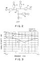
- FIG. 2 is a circuit diagram of the first preferred embodiment of a semiconductor integrated circuit according to the present invention.
- a semiconductor integrated circuit of FIG. 2 there is shown a principal part of an IC for ASK (Amplitude Shift Keying) modulation using a MES type FET made of a compound semiconductor (e.g., GaAs).
- ASK Amplitude Shift Keying
- the circuit of FIG. 2 is characterized in that an inductor element (coil) 1 is provided between the source terminal and ground terminal of an FET 10.
- an Lo input matching circuit 2 is provided between the gate terminal and input terminal IN of the FET 10.
- the gate terminal of the FET 10 is connected to a bias supply circuit 3.
- an RF output matching circuit 4 is provided between the drain terminal and output terminal OUT of the FET 10.
- the drain terminal of the FET 10 is connected to a control signal input circuit 5.
- the source terminal of the FET 10 is connected to a bias supply circuit 6.
- control signals from the control signal input circuit 5 the magnitude relationship between a drain voltage and source voltage of the FET 10 can be optionally switched and controlled.
- bias signals from the bias circuits the bias conditions of the FET 10 can be set to be optimum bias conditions.
- the inductance value of the inductor element 1 provided between the source terminal and ground terminal of the FET 10 is set so that the inductor element 1 series-resonates with a reactance component of a gate-to-source impedance of the FET 10. If such a series resonance occurs, no signal is transmitted to the output side of the FET 10, so that it is possible to reduce the amount of signal transmission.
- R can be approximated by expression (7).
- F ⁇ 2 ⁇ Cgd ⁇ Rds ⁇ (Cgs + Cgd) - ⁇ 2 ⁇ Cgd ⁇ Cgs ⁇ Rds ⁇ / [( ⁇ 2 ⁇ Cgd ⁇ Cgs ⁇ Rds) 2 + ⁇ ⁇ (Cgs + Cgd) ⁇ 2 ]
- Q ⁇ L / R
- FIG. 3 shows transfer characteristics (S21) of the FET 10 of FIG. 2.
- curve a denotes an On characteristic
- curve b denotes an OFF characteristic.
- the axis of abscissas denotes frequencies (GHz)
- the axis of ordinates denotes signal strengths (dB).
- FIG. 3 shows an example where the FET 10 of FIG. 2 is formed supposing that a working band is in the range of 5 GHz to 6 GHz. As shown in this figure, it can be seen that the amount of signal transmission decreases to (-15 dB) or less in a frequency band of 5 to 6 GHz when the FET 10 is in the OFF state.
- control signal input circuit 5 sets the drain-to-source voltage of the FET 10 so that Cgd / (Cgd + Cgs) ⁇ Rds / (Rds + RL) is minimum when the FET 10 is in the OFF state.
- the inductor element 1 is provided between the source terminal and ground terminal of the FET 10, and the inductor element 1 resonate in series for the gate-to-source impedance of the FET 10, so that it is possible to sufficiently decrease the amount of signal transmission when the FET 10 is in the OFF state.
- a capacitor element is provided between the gate terminal and source terminal of the FET 10 in addition to the above described inductor element 1.
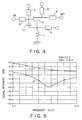
- FIG. 4 is a circuit diagram of the second preferred embodiment of a semiconductor integrated circuit according to the present invention.
- the same reference numbers are given to the same elements as those in FIG. 2, and different points will be mainly described below.
- the semiconductor integrated circuit of FIG. 4 has a capacitor element (second capacitor element) C1 provided between the gate terminal and source terminal of the FET 10, in addition to the construction of FIG. 2.
- a capacitor element (second capacitor element) C1 provided between the gate terminal and source terminal of the FET 10, in addition to the construction of FIG. 2.
- the reactance component of the FET 10 is expressed by expression (9).
- Xc ⁇ - ⁇ ⁇ (Cgd + Cgs + ci) - ⁇ 3 ⁇ Cgd 2 ⁇ (Cgs + Ci) ⁇ Rds 2 ⁇ / [ ⁇ 2 ⁇ Cgd ⁇ (Cgs + Ci) ⁇ Rds ⁇ 2 + ⁇ ⁇ (Cgs + Ci + Cgd) ⁇ 2 ]
- a resistance component R can be approximated by expression (10).
- F ⁇ 2 ⁇ Cgd ⁇ Rds ⁇ (Cgs + Ci + Cgd) - ⁇ 2 ⁇ Cgd ⁇ (Cgs + Ci) ⁇ Rds ⁇ / [ ⁇ 2 ⁇ Cgd ⁇ (Cgs + Ci) ⁇ Rds ⁇ 2 + ⁇ ⁇ (Cgs + Ci + Cgd) ⁇ 2 ]
- Q is expressed by ⁇ L/R.
- FIG. 5 shows transfer characteristics (S21) of the FET 10 of FIG. 4.
- curve c denotes an On characteristic
- curve d denotes an OFF characteristic.
- FIG. 5 shows an example where the FET 10 of FIG. 4 is formed supposing that a working band is in the range of 5 GHz to 6 GHz. As shown in this figure, it can be seen that the amount of signal transmission decreases to (-20 dB) or less in a frequency band of 5 to 6 GHz when the FET 10 is in the OFF state.
- the capacitor element C1 is provided between the gate terminal and source terminal of the FET 10, it is possible to apparently decrease the parasitic resistance component of the FET 10, and the signal attenuation can be smaller than that in the first preferred embodiment.
- a capacitor element is provided between the drain terminal and source terminal of the FET 10, in addition to the above described inductor element 1.
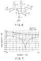
- FIG. 6 is a circuit diagram of the third preferred embodiment of a semiconductor integrated circuit according to the present invention.
- the same reference numbers are given to the same elements as those in FIG. 2, and different points will be mainly described below.
- the semiconductor integrated circuit of FIG. 6 has a capacitor element (third capacitor element) C2 provided between the drain terminal and source terminal of the FET 10, in addition to the construction of FIG. 2.
- a capacitor element (third capacitor element) C2 provided between the drain terminal and source terminal of the FET 10, in addition to the construction of FIG. 2.
- Xc -[( ⁇ 2 ⁇ Co ⁇ Cgd ⁇ Rds 2 + ⁇ 2 ⁇ Co 2 ⁇ Rds 2 + 1) ⁇ ⁇ ( ⁇ ⁇ Cgd + ⁇ 3 ⁇ Co 2 ⁇ Cgd ⁇ Rds 2 ) + Cgs ⁇ ( ⁇ 3 ⁇ Co ⁇ Cgd ⁇ Rds 2 + ⁇ 3 ⁇ Co 2 ⁇ Rds + ⁇ ) ⁇ - ( ⁇ 3 ⁇ Cgd 2 ⁇ Rds ⁇ Cgs)]
- a resistance component R can be approximated by expression (12).
- F [( ⁇ ⁇ Cgd ⁇ Rds) ⁇ ⁇ ( ⁇ ⁇ Cgd + ⁇ 3 ⁇ Co 2 ⁇ Cgd ⁇ Rds 2 ) + Cgs ⁇ ( ⁇ 3 ⁇ Co ⁇ Cgd ⁇ Rds 2 + ⁇ 3 ⁇ Co 2 ⁇ Rds + ⁇ ) ⁇ + ( ⁇ 2 ⁇ Co ⁇ Cgd ⁇ Rds 2 + ⁇ 2 ⁇ Co ⁇ Rds + 1) ⁇ ( ⁇ 2 ⁇ Cgd ⁇ Cgs)]
- Q is expressed by ⁇ L/R.
- FIG. 7 shows transfer characteristics (S21) of the FET 10 of FIG. 6.
- curve e denotes an On characteristic
- curve f denotes an OFF characteristic.
- FIG. 7 shows an example where the FET 10 of FIG. 6 is formed supposing that a working band is in the range of 5 GHz to 6 GHz. As shown in this figure, it can be seen that the amount of signal transmission decreases to (-25 dB) or less in a frequency band of 5 to 6 GHz when the FET 10 is in the OFF state.
- the capacitor element is provided between the drain terminal and source terminal of the FET 10, it is possible to apparently decrease the parasitic resistance component of the FET 10, and the signal attenuation can be smaller than that in the first preferred embodiment.
- the fourth preferred embodiment is a combination of the first through third preferred embodiment.
- FIG. 8 is a circuit diagram of the fourth preferred embodiment of a semiconductor integrated circuit according to the present invention.
- the same reference numbers are given to the same elements as those in FIGS. 4 and 6, and different points will be mainly described below.
- the semiconductor integrated circuit of FIG. 8 has a capacitor element C1 provided between the gate terminal and source terminal of the FET 10, and a capacitor element C2 provided between the drain terminal and source terminal of the FET 10, in addition to the construction of FIG. 2. Both of these capacitor elements C1 and C2 are provided for apparently decreasing the parasitic resistance component of the FET 10.
- the reactance component Xc of the FET 10 of FIG. 8 is expressed by expression (13).
- Xc -[( ⁇ 2 ⁇ Co ⁇ Cgd ⁇ Rds 2 + ⁇ 2 ⁇ Co 2 ⁇ Rds 2 + 1) ⁇ ⁇ ( ⁇ ⁇ Cgd + ⁇ 3 ⁇ Co 2 ⁇ Cgd ⁇ Rds 2 ) + (Ci + Cgs) ⁇ ( ⁇ 3 ⁇ Co ⁇ Cgd ⁇ Rds 2 + ⁇ 3 ⁇ Co 2 ⁇ Rds + ⁇ ) ⁇ - ⁇ 3 ⁇ Cgd 2 ⁇ Rds ⁇ (Ci + Cgs) ⁇ ] / [( ⁇ ⁇ Cgd + ⁇ 3 ⁇ Co 2 ⁇ Cgs ⁇ Rds 2 ) + (Ci + Cgs) ⁇ ( ⁇ 3 ⁇ Co ⁇ Cgd ⁇ Rds 2 + ⁇ 3 ⁇ Co 2 ⁇ Rds + ⁇ ) ⁇ 2 + ⁇ 2 ⁇
- a resistance component R can be approximated by expression (14).
- F [( ⁇ ⁇ Cgd ⁇ Rds) ⁇ ⁇ ( ⁇ ⁇ Cgd + ⁇ 3 ⁇ Co 2 ⁇ Cgd ⁇ Rds 2 ) + (Ci + Cgs) ⁇ ( ⁇ 3 ⁇ Co ⁇ Cgd ⁇ Rds 2 + ⁇ 3 ⁇ Co 2 ⁇ Rds + ⁇ ) ⁇ + ( ⁇ 2 ⁇ Co ⁇ Cgd ⁇ Rds 2 + ⁇ 2 ⁇ Co ⁇ Rds + 1) ⁇ ⁇ 2 ⁇ Cgd ⁇ (Ci + Cgs) ⁇ ]
- Q is expressed by ⁇ L/R.
- FIG. 9 shows transfer characteristics (S21) of the FET 10 of FIG. 8.
- curve g denotes an On characteristic
- curve h denotes an OFF characteristic.
- FIG. 9 shows an example where the FET 10 of FIG. 8 is formed supposing that a working band is in the range of 5 GHz to 6 GHz. As shown in this figure, it can be seen that the amount of signal transmission decreases to (-30 dB) or less in a frequency band of 5 to 6 GHz when the FET 10 is in the OFF state.
- capacitor elements C1 and C2 are provided between the gate terminal and source terminal of the FET 10 and between the drain terminal and source terminal of the FET 10, it is possible to decrease the parasitic resistance component of the FET 10, and the signal attenuation can be smaller than those in the first though third preferred embodiments.
- the inductor element 1 is provided between the source terminal and ground terminal of the FET 10 in the first through fourth preferred embodiments, there is a problem in that continuous currents flow from the bias supply circuit 6, which is connected to the source terminal, to the ground terminal via the inductor element 1, so that electric power consumption increases. Therefore, in the fifth preferred embodiment, the currents are interrupted.
- FIG. 10 is a circuit diagram of the fifth preferred embodiment of a semiconductor integrated circuit according to the present invention.
- the same reference numbers are given to the same elements as those in FIG. 8, and different points will be mainly described below.
- the semiconductor integrated circuit of FIG. 10 is characterized in that an inductor element 1 is connected to a capacitor element (first capacitor element) C3 in series between the source terminal and ground terminal of an FET 10. Specifically, the capacitor element C3 is added to the construction of FIG. 8.
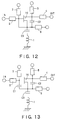
- FIG. 10 has shown the example where the capacitor element C3 is added to the circuit of FIG. 8, it is possible to reduce electric power consumption by adding the capacitor element C3 in FIGS. 2, 4 and 6.
- FIG. 11 shows an example where the capacitor element C3 is added to the circuit of FIG. 2
- FIG. 12 shows an example where the capacitor element C3 is added to the circuit of FIG. 4
- FIG. 13 shows an example where the capacitor element C3 is added to the circuit of FIG. 6.
- the present invention can be utilized for other purposes than the ASK modulation.
- the present invention may be applied to a switch formed of an FET.
- control signal input circuit 5 and the bias supply circuits 3 and 6 have been connected to the respective terminals of the FET 10 in the above described preferred embodiments, the control signal input circuit 5 and the bias supply circuits 3 and 6 may be connected only to part of terminals of the FET 10.
Landscapes
- Networks Using Active Elements (AREA)
- Amplifiers (AREA)
- Digital Transmission Methods That Use Modulated Carrier Waves (AREA)
- Semiconductor Integrated Circuits (AREA)
Applications Claiming Priority (2)
| Application Number | Priority Date | Filing Date | Title |
|---|---|---|---|
| JP2000126006A JP3840361B2 (ja) | 2000-04-26 | 2000-04-26 | 半導体集積回路 |
| JP2000126006 | 2000-04-26 |
Publications (1)
| Publication Number | Publication Date |
|---|---|
| EP1150430A1 true EP1150430A1 (en) | 2001-10-31 |
Family
ID=18635863
Family Applications (1)
| Application Number | Title | Priority Date | Filing Date |
|---|---|---|---|
| EP01110029A Withdrawn EP1150430A1 (en) | 2000-04-26 | 2001-04-26 | Semiconductor integrated circuit |
Country Status (4)
| Country | Link |
|---|---|
| US (1) | US6822489B2 (enExample) |
| EP (1) | EP1150430A1 (enExample) |
| JP (1) | JP3840361B2 (enExample) |
| KR (1) | KR100372534B1 (enExample) |
Families Citing this family (1)
| Publication number | Priority date | Publication date | Assignee | Title |
|---|---|---|---|---|
| JP4885034B2 (ja) * | 2007-03-30 | 2012-02-29 | シャープ株式会社 | Ask変調回路および送信装置 |
Citations (4)
| Publication number | Priority date | Publication date | Assignee | Title |
|---|---|---|---|---|
| US5475875A (en) * | 1993-06-17 | 1995-12-12 | Oki Electric Industry Co., Ltd. | Antenna switching circuit employing FETs for reduced power consumption |
| JPH1013204A (ja) * | 1996-06-25 | 1998-01-16 | New Japan Radio Co Ltd | 半導体スイッチ回路 |
| JPH10336000A (ja) * | 1997-06-05 | 1998-12-18 | Nec Eng Ltd | 高周波信号切り替え器 |
| EP0993120A2 (en) * | 1998-10-07 | 2000-04-12 | Murata Manufacturing Co., Ltd. | SPST switch, SPDT switch, and communication apparatus using the SPDT switch |
Family Cites Families (15)
| Publication number | Priority date | Publication date | Assignee | Title |
|---|---|---|---|---|
| US4166965A (en) | 1977-12-02 | 1979-09-04 | Rca Corporation | Threshold gate |
| US4338582A (en) * | 1978-09-29 | 1982-07-06 | Rca Corporation | Electronically tunable resonator circuit |
| US4454485A (en) * | 1981-08-05 | 1984-06-12 | The United States Of America As Represented By The Secretary Of The Army | Low distortion FET oscillator with feedback loop for amplitude stabilization |
| US4696639A (en) * | 1986-11-06 | 1987-09-29 | Honeywell Inc. | Self-energizing burner control system for a fuel burner |
| US5200713A (en) | 1990-10-04 | 1993-04-06 | Wiltron Company | Multiple magnetically tuned oscillator |
| FR2672449A1 (fr) * | 1991-02-06 | 1992-08-07 | Alcatel Espace | Dephaseur variable analogique pour signaux hyperfrequence. |
| US5693080A (en) * | 1993-03-19 | 1997-12-02 | Wallsten Medical S.A. | Apparatus for medical treatment |
| US5345123A (en) * | 1993-07-07 | 1994-09-06 | Motorola, Inc. | Attenuator circuit operating with single point control |
| JPH07303001A (ja) * | 1994-05-10 | 1995-11-14 | Hitachi Ltd | 高周波スイッチ |
| KR100413745B1 (ko) * | 1995-08-30 | 2004-03-20 | 정규범 | 컨버터스위치의스위칭손실및노이즈저감회로 |
| US5821815A (en) * | 1996-09-25 | 1998-10-13 | Endgate Corporation | Miniature active conversion between slotline and coplanar waveguide |
| JP3087844B2 (ja) * | 1997-12-26 | 2000-09-11 | 日本電気株式会社 | 半導体移相器 |
| JPH11298295A (ja) * | 1998-04-10 | 1999-10-29 | Mitsubishi Electric Corp | 不平衡−平衡変換器及びバランス形ミクサ |
| US5986518A (en) * | 1998-06-30 | 1999-11-16 | Motorola, Inc. | Distributed MMIC active quadrature hybrid and method for providing in-phase and quadrature-phase signals |
| JP2000022511A (ja) * | 1998-07-01 | 2000-01-21 | Mitsubishi Electric Corp | パワートランジスタ制御回路 |
-
2000
- 2000-04-26 JP JP2000126006A patent/JP3840361B2/ja not_active Expired - Fee Related
-
2001
- 2001-04-25 KR KR10-2001-0022323A patent/KR100372534B1/ko not_active Expired - Fee Related
- 2001-04-25 US US09/841,595 patent/US6822489B2/en not_active Expired - Fee Related
- 2001-04-26 EP EP01110029A patent/EP1150430A1/en not_active Withdrawn
Patent Citations (4)
| Publication number | Priority date | Publication date | Assignee | Title |
|---|---|---|---|---|
| US5475875A (en) * | 1993-06-17 | 1995-12-12 | Oki Electric Industry Co., Ltd. | Antenna switching circuit employing FETs for reduced power consumption |
| JPH1013204A (ja) * | 1996-06-25 | 1998-01-16 | New Japan Radio Co Ltd | 半導体スイッチ回路 |
| JPH10336000A (ja) * | 1997-06-05 | 1998-12-18 | Nec Eng Ltd | 高周波信号切り替え器 |
| EP0993120A2 (en) * | 1998-10-07 | 2000-04-12 | Murata Manufacturing Co., Ltd. | SPST switch, SPDT switch, and communication apparatus using the SPDT switch |
Non-Patent Citations (2)
| Title |
|---|
| PATENT ABSTRACTS OF JAPAN vol. 1998, no. 05 30 April 1998 (1998-04-30) * |
| PATENT ABSTRACTS OF JAPAN vol. 1999, no. 03 31 March 1999 (1999-03-31) * |
Also Published As
| Publication number | Publication date |
|---|---|
| KR20010098869A (ko) | 2001-11-08 |
| US6822489B2 (en) | 2004-11-23 |
| US20020000620A1 (en) | 2002-01-03 |
| JP2001308941A (ja) | 2001-11-02 |
| KR100372534B1 (ko) | 2003-02-15 |
| JP3840361B2 (ja) | 2006-11-01 |
Similar Documents
| Publication | Publication Date | Title |
|---|---|---|
| US20010040479A1 (en) | Electronic switch | |
| US6496684B2 (en) | SPST switch, SPDT switch, and communication apparatus using the SPDT switch | |
| JP2848502B2 (ja) | マイクロ波半導体スイッチ | |
| KR102666474B1 (ko) | 주파수 선택성 임피던스 정합 네트워크를 갖춘 rf 전력 증폭기 | |
| EP0609746A1 (en) | Microwave switch circuit and an antenna apparatus | |
| JPH11274804A (ja) | 高周波スイッチ | |
| JP3263798B2 (ja) | 半導体スイツチ | |
| JPH09284170A (ja) | アンテナスイッチ及びスイッチ・パワーアンプ一体型半導体装置 | |
| EP1169776B1 (en) | Biasing arrangement for field effect transistors | |
| US10622961B2 (en) | Reflection type phase shifter with active device tuning | |
| US20080106353A1 (en) | High-frequency switch | |
| EP1150430A1 (en) | Semiconductor integrated circuit | |
| JPH10336000A (ja) | 高周波信号切り替え器 | |
| JPH1013204A (ja) | 半導体スイッチ回路 | |
| US5406151A (en) | Semiconductor switching circuit | |
| JPH01173908A (ja) | 発振装置 | |
| JP3836044B2 (ja) | スイッチ回路 | |
| KR100392208B1 (ko) | 무선 주파수 전력 증폭기용 바이어싱 회로 | |
| JP2007312003A (ja) | アッテネータ | |
| JP3670084B2 (ja) | 半導体スイッチ回路 | |
| JP3922950B2 (ja) | 周波数変換回路 | |
| KR102684762B1 (ko) | 초고주파대역 스위치 회로 | |
| JP3929732B2 (ja) | 半導体集積回路 | |
| US10218353B2 (en) | Low distortion RF switch | |
| JPH11261396A (ja) | 高周波スイッチ装置 |
Legal Events
| Date | Code | Title | Description |
|---|---|---|---|
| PUAI | Public reference made under article 153(3) epc to a published international application that has entered the european phase |
Free format text: ORIGINAL CODE: 0009012 |
|
| 17P | Request for examination filed |
Effective date: 20010426 |
|
| AK | Designated contracting states |
Kind code of ref document: A1 Designated state(s): AT BE CH CY DE DK ES FI FR GB GR IE IT LI LU MC NL PT SE TR Kind code of ref document: A1 Designated state(s): DE FR GB |
|
| AX | Request for extension of the european patent |
Free format text: AL;LT;LV;MK;RO;SI |
|
| AKX | Designation fees paid |
Free format text: DE FR GB |
|
| 17Q | First examination report despatched |
Effective date: 20020619 |
|
| GRAP | Despatch of communication of intention to grant a patent |
Free format text: ORIGINAL CODE: EPIDOSNIGR1 |
|
| STAA | Information on the status of an ep patent application or granted ep patent |
Free format text: STATUS: THE APPLICATION IS DEEMED TO BE WITHDRAWN |
|
| 18D | Application deemed to be withdrawn |
Effective date: 20050126 |