EP1148149A2 - Procédé de production des systèmes multicouches - Google Patents
Procédé de production des systèmes multicouches Download PDFInfo
- Publication number
- EP1148149A2 EP1148149A2 EP01109003A EP01109003A EP1148149A2 EP 1148149 A2 EP1148149 A2 EP 1148149A2 EP 01109003 A EP01109003 A EP 01109003A EP 01109003 A EP01109003 A EP 01109003A EP 1148149 A2 EP1148149 A2 EP 1148149A2
- Authority
- EP
- European Patent Office
- Prior art keywords
- layer
- reflectivity
- deposition
- layers
- time
- Prior art date
- Legal status (The legal status is an assumption and is not a legal conclusion. Google has not performed a legal analysis and makes no representation as to the accuracy of the status listed.)
- Granted
Links
Images


Classifications
-
- C—CHEMISTRY; METALLURGY
- C23—COATING METALLIC MATERIAL; COATING MATERIAL WITH METALLIC MATERIAL; CHEMICAL SURFACE TREATMENT; DIFFUSION TREATMENT OF METALLIC MATERIAL; COATING BY VACUUM EVAPORATION, BY SPUTTERING, BY ION IMPLANTATION OR BY CHEMICAL VAPOUR DEPOSITION, IN GENERAL; INHIBITING CORROSION OF METALLIC MATERIAL OR INCRUSTATION IN GENERAL
- C23C—COATING METALLIC MATERIAL; COATING MATERIAL WITH METALLIC MATERIAL; SURFACE TREATMENT OF METALLIC MATERIAL BY DIFFUSION INTO THE SURFACE, BY CHEMICAL CONVERSION OR SUBSTITUTION; COATING BY VACUUM EVAPORATION, BY SPUTTERING, BY ION IMPLANTATION OR BY CHEMICAL VAPOUR DEPOSITION, IN GENERAL
- C23C14/00—Coating by vacuum evaporation, by sputtering or by ion implantation of the coating forming material
- C23C14/58—After-treatment
- C23C14/5873—Removal of material
-
- B—PERFORMING OPERATIONS; TRANSPORTING
- B82—NANOTECHNOLOGY
- B82Y—SPECIFIC USES OR APPLICATIONS OF NANOSTRUCTURES; MEASUREMENT OR ANALYSIS OF NANOSTRUCTURES; MANUFACTURE OR TREATMENT OF NANOSTRUCTURES
- B82Y10/00—Nanotechnology for information processing, storage or transmission, e.g. quantum computing or single electron logic
-
- C—CHEMISTRY; METALLURGY
- C23—COATING METALLIC MATERIAL; COATING MATERIAL WITH METALLIC MATERIAL; CHEMICAL SURFACE TREATMENT; DIFFUSION TREATMENT OF METALLIC MATERIAL; COATING BY VACUUM EVAPORATION, BY SPUTTERING, BY ION IMPLANTATION OR BY CHEMICAL VAPOUR DEPOSITION, IN GENERAL; INHIBITING CORROSION OF METALLIC MATERIAL OR INCRUSTATION IN GENERAL
- C23C—COATING METALLIC MATERIAL; COATING MATERIAL WITH METALLIC MATERIAL; SURFACE TREATMENT OF METALLIC MATERIAL BY DIFFUSION INTO THE SURFACE, BY CHEMICAL CONVERSION OR SUBSTITUTION; COATING BY VACUUM EVAPORATION, BY SPUTTERING, BY ION IMPLANTATION OR BY CHEMICAL VAPOUR DEPOSITION, IN GENERAL
- C23C14/00—Coating by vacuum evaporation, by sputtering or by ion implantation of the coating forming material
- C23C14/22—Coating by vacuum evaporation, by sputtering or by ion implantation of the coating forming material characterised by the process of coating
- C23C14/54—Controlling or regulating the coating process
- C23C14/542—Controlling the film thickness or evaporation rate
- C23C14/545—Controlling the film thickness or evaporation rate using measurement on deposited material
- C23C14/547—Controlling the film thickness or evaporation rate using measurement on deposited material using optical methods
-
- G—PHYSICS
- G21—NUCLEAR PHYSICS; NUCLEAR ENGINEERING
- G21K—TECHNIQUES FOR HANDLING PARTICLES OR IONISING RADIATION NOT OTHERWISE PROVIDED FOR; IRRADIATION DEVICES; GAMMA RAY OR X-RAY MICROSCOPES
- G21K1/00—Arrangements for handling particles or ionising radiation, e.g. focusing or moderating
- G21K1/06—Arrangements for handling particles or ionising radiation, e.g. focusing or moderating using diffraction, refraction or reflection, e.g. monochromators
- G21K1/062—Devices having a multilayer structure
-
- G—PHYSICS
- G21—NUCLEAR PHYSICS; NUCLEAR ENGINEERING
- G21K—TECHNIQUES FOR HANDLING PARTICLES OR IONISING RADIATION NOT OTHERWISE PROVIDED FOR; IRRADIATION DEVICES; GAMMA RAY OR X-RAY MICROSCOPES
- G21K2201/00—Arrangements for handling radiation or particles
- G21K2201/06—Arrangements for handling radiation or particles using diffractive, refractive or reflecting elements
- G21K2201/067—Construction details
Definitions
- the invention relates to a method for the production of multi-layer systems with N layers having predertermined thicknesses, especially for the production of multi-layer systems for wavelength ranges in the extreme ultraviolet and soft X-ray wavelength range, in which N layers are deposited and if need be one or more layer are partially removed after deposition and in which at the same time as deposition and/or removal of layers, the layers' reflectivity dependent on layer thickness is measured.
- the layering consists of a number of alternating layers of two or more materials, which have different refractive indices.
- d d A + d B is the sum of the individual layer thicknesses of the materials A and B, ⁇ the wavelength, ⁇ m the angle of incidence and m the order of diffraction.
- the maximum reflectivity can be optimised by two opposite possibilities.
- One possibility consists of using materials whose refractive indices differ from each other as much as possible.
- the layers all have the same optical thickness. In the case of an angle of incidence of 90° the layer thickness corresponds to a quarter of the wavelength which is reflected in phase.
- the other possibility consists of reproducing an "ideal Bragg crystal", in which layers of absorbent material, which are as thin as possible, preferably atomic mono-layers, alternate with thick layers of non-absorbent material. Losses due to absorption are minimised, by disposing the thin absorbent layers in the nodal planes of the standing waves, which are produced by the incident and reflected beam.
- X-ray mirrors are used for example in X-ray fluorescence analysis and X-ray astronomy.
- a commercially highly significant deposition of interference mirrors in the X-ray and ultraviolet range is semi-conductor lithography.
- optical elements made from multi-component multi-layer systems are used primarily to reproduce semi-conductor circuit structures on wafers.
- Deviations from the theoretical reflectivity of an interference system result primarily from flaws in the thickness of the individual layers. This problem becomes even more serious if the number of layers is very high. Also the roughness of the interfaces between the individual layers reduces reflectivity as the intensity is reduced by scatter on the surface roughnesses.
- the patent specification DE 27 50 421 C2 describes a measuring method and measuring device for the production of multi-layer systems for the visible wavelength range.
- alternating layers with high and low refractivity are applied to transparent substrates.
- the layers are each applied to one test glass per material, the test glasses being exposed to the same coating material flow as the substrates.
- the transmission and/or reflection behaviour of the layers is continuously registered.
- the test glass just being coated is impinged upon by a monochromatic light beam and the proportion of light reflected or passing through is measured.
- the layer thickness from the reflectivity advantage is taken of the fact that the light beam which is reflected on the upper surface of the layer and the light beam which is reflected on the undersurface of the layer, i.e. in the case of test glasses the interface between layer material and glass, are superimposed. Depending on the relative retardation or phase difference of these two beams, negative or positive interference phenomena will be obtained.
- the reflectivity depends sinusoidally on the layer thickness.
- the reflectivity measurement result will thus be used for definite interruption of the coating process.
- the multi-layer systems produced have constant layer thicknesses of ⁇ /4.
- ⁇ is the wavelength which will be the wavelength in the case of later use, as well as the wavelength with which the reflectivity is measured.
- the coating process is always interrupted either at maximum or minimum reflectivity. The extrema can be registered manually or automatically for the visible wavelength range sufficiently accurately without great expense.
- the "minimum-maximum method” is also applied in the US 5,551,587, the US 5,151,295 and the JP 61296305 A.
- the thickness of the deposited layer is parametrised by the deposition time.
- two beams of different wavelengths are used to measure the transmission dependent on the time during the deposition of the layers. This improves the accuracy of the determination of the peak values of the transmission.
- the actual deposition stop occurs slightly after the respective peak values.
- the special feature of the US 5,551,587 is to manufacture a multilayer mirror by stimulation of the penetration of one of the materials into the layer with the other material after which the original layer thickness of the first material is removed by etching.
- the JP 63028862 A improves the accuracy of the "minimum-maximum method" by fitting the measured transmittivity or reflectivity data by quadratic regression.
- the target vapor deposition time of the layer is based on the value obtained.
- extreme ultraviolet and soft X-ray range should here be understood to mean the wavelengths of an order of magnitude between one-tenth and ten nm. Also in the case of production of interference systems for this short-wave wavelength range, the reflectivity is measured in situ, essentially using light of a wavelength that is comparable with that of the final deposition (i.e. soft X-ray range or extreme ultraviolet range), the thickness of the top layer is deduced from the reflectivity and one changes over between the coating with one or other material at the extrema.
- the layer thickness is monitored not only via the reflectivity, but also via a quartz crystal monitor. It is a matter of special interference systems in which the absorbing layer is too thin for its thickness to be determined by means of reflectivity measurements.
- the problem of the present invention is to find a method for controlling the layer thickness when applying and, if necessary, removing thin layers, especially in the production of interference systems for reflection of wavelengths in the extreme ultraviolet and soft X-ray wavelength range, with the help of which interference systems can be produced, which on the whole have higher reflectivities and improved wavelength selectivity.
- off-extrema method switching is done when the reflected amplitude from the top layer is partly out of phase with the reflected amplitude from the stack underneath.
- the phase shift is correlated to a certain intensity variation of the monitor signal and corresponds to the design parameters of the particular multerlayer structure.
- the wavelength of X-ray source or angle of monitoring are adjusted.
- the new method allows switching at arbitrary moments in the monitoring and control process, moments being fully determined by the multilayer design parameters.
- the method can be applied, but is not limited, to coating processes based on electron-beam evaporation or ion-beam evaporation/sputtering.
- the reflectivity of the layer system is measured.
- a test substrate for measuring reflection offers itself if the individual components of the coating plant are disposed in such a way that light source, substrate and detector cannot be ideally oriented relative to each other. In the case of use of a test substrate it must however be guaranteed that the test substrate is exposed to the same material flow as the actual substrate. With the method according to the invention a single test substrate is sufficient, to which all the layers are applied. The reflectivity measurement is always carried out with a monochromatic beam.
- a reflectivity curve dependent on the thickness is calculated.
- the layer thickness for its part depends on the coating time.
- the exact connection between layer thickness and coating time is determined by the coating process. In a first approximation a linear connection can be assumed. Where time and/or points in time are referred to below, this should be understood to mean a parametrisation of the layer thickness. Other parametrisations are also possible.
- the point in time t i is selected for each layer i, in such a way that the phase difference of the beams reflecting at the surface and the undersurface amounts to zero or an integral multiple of ⁇ /2.
- the point in time t i should then essentially lie within the range of a turning point of the reflectivity curve, i.e. in the steepest range, in which the sensitivity to the direct determination of the point in time t i is greatest during the measuring process. This reduces the errors in the layer thickness of the individual layers i.
- the points in time at which the extrema are present shall advantageously be designated T 1 .
- the change-over point in time t 1 should always be defined in relation to the previous extremum in time T 1 .
- the advantage lies in the fact that during measurement of the reflectivity and the layer thickness, the extremum can be determined as accurately as possible, as a data range can be used for the evaluation, in which the extremum does not lie at the range limit. It is then possible to determine t 1 with corresponding accuracy.
- the selection of the means for calculating the point in time t i should take into consideration the fact that the time interval up to determination of the point in time T i must be smaller than the time interval between T i and t i . Except with very high coating rates and very thin layers this should not represent any problem.
- the position of the extremum can be determined more accurately, and the position of the point in time t i can also be determined more accurately with simultaneous reflectivity measurement, as it lies in the steeper range of the reflectivity curve.
- the greater accuracy of the layer thicknesses in the method according to the invention makes it possible to produce interference systems which have improved reflectivity.
- deposition of the first layer is commenced.
- the reflectivity of this layer or the equivalent layer on a test substrate is measured.
- the point in time T i i.e. the position of the extreme point of the reflectivity curve for this layer i is determined from the measured data.
- the point in time T is passed, as soon as the point in time t i is reached, deposition of the layer is stopped.
- the method is indepent of time, i.e. of points in time t i and t i ', because the points in time are used of define the parameter k i and k i '.
- the deposition and partial removal are stopped when the current parameters k c/i and k c'/i reach the parameters k i and k i ' respectively. If the deposition rate or the removal rate are not constant during deposition or removal the predetermined deposition or removal time would not be met. As the deposition or removal is correlated to the time-independent parameters k c/i and k c'/i the precision can be observed in any case.
- parameters k i and k i ' is based on an apse and on the starting and terminal value in the neighbourhood of the apse and/or on a second apse in the interval t i - t i-1 .
- the parameters k i and k i ' for two materials of a multi-layer system are defined as follows:
- k i , k i ' values can differ from one period to another depending on the particular multilayer design.
- the real monitoring curve can deviate somewhat from the simulated one. Consequently, different procedures of the switching point determination in the monitoring process can lead to slightly different precision of the control.
- These process steps can be transferred to a control device.
- coating parameters are stored in the control device.
- the control device determines T 1 from the reflectivity data, and compares the coating parameters with the measured values, to ascertain whether the point in time t i or k i is already reached and deposition must be stopped. In this way the method according to the invention can be fully automated, which makes it of interest for large-scale industrial use in semi-conductor lithography.
- the reflectivity is also enhanced in that the surface of a layer i may be polished before the layer i + 1 is applied. Also the points in time t 1 ' or k i ', at which the deposition is stopped, should be established in advance on the basis of the calculated reflectivity curve. In this connection it is to be noted that the removal resulting from polishing is taken into consideration in the layer thickness to be applied. This means that slightly more should be applied than the desired layer thickness.
- polishing, involving some removal, of layer i is planned, this is now carried out from the point in time t i up to the point in time t i ' or k i '. This can also be carried out by the control device.
- a quartz crystal monitor or a mass spectrometer can be used for rough monitoring of the layer thicknesses.
- the layer thicknesses should be selected between 0.1 nm and 50 nm. Especially preferable are layer thicknesses between 1 nm and 30 nm.
- the wavelength of the beam of the reflectivity measurement lies between 2 nm and 200 nm.
- the angle of incidence is selected corresponding to the wavelength and the thickness of the layers.
- a major advantage over the conventional methods is that the selection of the wavelength, and of the angle of incidence of the monochromatic light beam for reflectivity measurement, is no longer limited by the measuring method itself, but now only by the experimental set-up.
- This makes it possible to produce interference systems with layer thickness conditions, which were not accessible with the conventional methods.
- the production of interference systems with non-constant layer thickness conditions or of non-plane or aspherical interference systems is greatly facilitated.
- variation of the layer thickness conditions throughout the total thickness of the interference system the reflectivity can be still further enhanced.
- the number of layers N should, advantageously, lie between 2 and 1000. Especially preferred are interference systems with 80 to 1000 layers. In particular the number of layers should be especially high in the case of extremely short wavelengths.
- Different methods can be used for deposition of the individual layers.
- Methods can be used which are based on thermal evaporation of the material or the sputtering method.
- the advantages of the sputtering method are that the sputtering process itself can be well controlled by means of well-defined ion energies and angles of incidence.
- Electron beam evaporation is preferably used.
- the advantages of electron beam evaporation are that most process parameters (energy, angle etc.) are independent of one another and can therefore be optimised individually.
- layers with little roughness are produced by depositing by evaporation.
- materials can be evaporated by electron beams or laser pulses.
- the quality of the films which are deposited by laser evaporation, with regard to the thickness and surface roughness, is better than in the case of electron beam evaporation, however the rate of depositing by evaporation is very much lower.
- depositing by evaporation can only be carried out within a limited solid angle, so that it is not possible to coat larger areas.
- T 1 , t i or t i ' As degradation of the reflectivity signal by noise cannot be fully suppressed, it has proved advantageous to determine the points in time T 1 , t i or t i ' by fitting the measured reflectivities dependent on time. For this, the method of least squares has proved particularly successful.
- the measured reflectivities are taken into consideration, which lie within a time interval lying approximately symmetrically around the extreme point. By fitting the data a point in time, T i , t i and t i ' is obtained from which the error resulting from the background noise has essentially been calculated out.
- ion beams For the removal of the layer i, the use of ion beams has proved successful. By using ion beams, material is removed and the surface polished simultaneously. In addition there is a kind of recrystallisation effect, which leads to the layer becoming denser at its surface, and hence more resistant to, for example, radiation damage.
- alternating layers of a strongly absorbent material and of a less absorbent material are applied.
- an ideal "Bragg crystal” is reproduced.
- transition metals and refractory metals or their compounds are chosen for the strongly absorbent material.
- Especially preferred in combination with the method according to the invention are: molybdenum, molybdenum carbide, molybdenum silicide, rheniumtungsten, tungsten, tungsten cabride, tungsten silicide, nickel or nickel silicide.
- the less absorbent materials chosen are predominantly light non-metals. Silicon, carbon, boron or even beryllium are preferred.
- the ratio of the layer thickness of the strongly absorbent material to the total of the layer thickness of the less absorbent material and layer thickness of the strongly absorbent material is preferably selected between 0.2 and 0.8.
- a gamma ratio between 0.35 and 0.45 is especially preferred.
- An advantage of the method according to the invention is that the gamma ratio can be adjusted as desired.
- the gamma ratio can be varied during the coating process, to produce especially optimised interference systems with especially high reflectivity.
- the production of interference systems with varying gamma ratios can be automated, without this requiring greater expense than in the case of conventional interference systems. This was not possible with the conventional methods.
- part of the layer is removed with an ion beam.
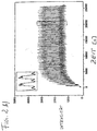
- the process changes over to depositing by evaporation of silicon. Initially the reflectivity rises somewhat to the maximum D, which, however, is not relevant for the control of this coating process. Subsequently the reflectivity declines as far as the minimum E, at which the beam reflected at the surface of the silicon layer and the beam reflected at the interface with the molybdenum are inversely phased and completely cancel each other out.
- the position of the minimum E is designated by the time T 2 .
- a ratio could also be formed with I C instead of I D .
- Figures 2a and 2b show actually measured reflectivity curves during production of an X-ray interference mirror.
- Fig. 2a alternating multi-layer layers of molybdenum and silicon were applied for 2 1/2 hours
- Fig. 2b an interference system was also produced from molybdenum and silicon in 7 hours.
- the reflectivity was measured at 3.16 nm in both cases.
- Fig. 2a the angle of incidence amounted to 16.88°
- Fig. 2b it amounted to 16.06°.
- the constants k 1 , k 2 , k 2 ' for the first ten periods are different to the constants for the following periods.
- k 1 0.23
- k 2 0.25
- k 2 ' 0.70
- the resulting phase thickness amounts to 6.40 nm
- the gamma ratio amounts to 0.363. In total 20 periods, i.e. 40 layers were applied.
- a reflectivity of 69.2% was achieved at 12.8 nm and 90°.
- a reflectivity of 69.4% was also achieved at 12.8 nm and 90°.
Applications Claiming Priority (2)
| Application Number | Priority Date | Filing Date | Title |
|---|---|---|---|
| DE10019045A DE10019045B4 (de) | 2000-04-18 | 2000-04-18 | Verfahren zum Herstellen von Viellagensystemen |
| DE10019045 | 2000-04-18 |
Publications (3)
| Publication Number | Publication Date |
|---|---|
| EP1148149A2 true EP1148149A2 (fr) | 2001-10-24 |
| EP1148149A3 EP1148149A3 (fr) | 2003-12-17 |
| EP1148149B1 EP1148149B1 (fr) | 2006-06-28 |
Family
ID=7639077
Family Applications (1)
| Application Number | Title | Priority Date | Filing Date |
|---|---|---|---|
| EP01109003A Expired - Lifetime EP1148149B1 (fr) | 2000-04-18 | 2001-04-11 | Procédé de production des systèmes multicouches |
Country Status (4)
| Country | Link |
|---|---|
| US (1) | US6483597B2 (fr) |
| EP (1) | EP1148149B1 (fr) |
| JP (1) | JP2002048902A (fr) |
| DE (2) | DE10019045B4 (fr) |
Cited By (5)
| Publication number | Priority date | Publication date | Assignee | Title |
|---|---|---|---|---|
| EP1278042A1 (fr) * | 2001-07-18 | 2003-01-22 | Alps Electric Co., Ltd. | Méthode pour former un film optique mince sur un substrat avec grande précision et son appareil associé |
| GB2388848A (en) * | 2002-05-24 | 2003-11-26 | Alps Electric Co Ltd | Control of optical thin film deposition |
| WO2012175494A1 (fr) * | 2011-06-22 | 2012-12-27 | Carl Zeiss Smt Gmbh | Procédé de production d'un élément optique réfléchissant pour lithographie uv extrême |
| US8927051B2 (en) | 2007-09-12 | 2015-01-06 | Flisom Ag | Method for manufacturing a compound film |
| CN109283203B (zh) * | 2017-07-19 | 2023-09-12 | 诺威有限公司 | 对图案化结构的基于x射线的测量 |
Families Citing this family (4)
| Publication number | Priority date | Publication date | Assignee | Title |
|---|---|---|---|---|
| US20070281109A1 (en) * | 2000-03-31 | 2007-12-06 | Carl Zeiss Smt Ag | Multilayer system with protecting layer system and production method |
| JP3632757B2 (ja) * | 2001-01-31 | 2005-03-23 | 古河電気工業株式会社 | 光学フィルタの製造方法 |
| EP1446811A1 (fr) * | 2001-10-24 | 2004-08-18 | Carl Zeiss SMT AG | Procede de fabrication de systemes multicouche |
| CN106017338B (zh) * | 2016-05-26 | 2018-08-24 | 国家纳米科学中心 | 一种确定薄膜连续性的临界厚度的方法 |
Citations (5)
| Publication number | Priority date | Publication date | Assignee | Title |
|---|---|---|---|---|
| DE2750421C2 (de) | 1977-11-11 | 1986-09-25 | Leybold-Heraeus GmbH, 5000 Köln | Meßverfahren und Meßvorrichtungen für die Herstellung von Vielfach-Schichtsystemen |
| JPS61296305A (ja) | 1985-06-25 | 1986-12-27 | Horiba Ltd | 多層膜干渉フイルタの製造方法 |
| JPS6328862A (ja) | 1986-07-23 | 1988-02-06 | Nippon Sheet Glass Co Ltd | 膜厚制御方法 |
| US5151295A (en) | 1990-06-11 | 1992-09-29 | Matsushita Electric Industrial Co., Ltd. | Process for manufacturing an optical recording medium |
| US5551587A (en) | 1993-10-08 | 1996-09-03 | U.S. Philips Corporation | Multilayer mirror with a variable refractive index |
Family Cites Families (9)
| Publication number | Priority date | Publication date | Assignee | Title |
|---|---|---|---|---|
| US4676646A (en) * | 1985-10-15 | 1987-06-30 | Energy Conversion Devices, Inc. | Method and apparatus for controlling thickness of a layer of an optical data storage device by measuring an optical property of the layer |
| US5310603A (en) * | 1986-10-01 | 1994-05-10 | Canon Kabushiki Kaisha | Multi-layer reflection mirror for soft X-ray to vacuum ultraviolet ray |
| US4909631A (en) * | 1987-12-18 | 1990-03-20 | Tan Raul Y | Method for film thickness and refractive index determination |
| CA1323234C (fr) * | 1989-09-21 | 1993-10-19 | Gordon G. Shepherd | Multicouches constituees de minces pellicules a variations de phases pour interferometres michelson |
| US5410411A (en) * | 1992-01-17 | 1995-04-25 | Matsushita Electric Industrial Co., Ltd. | Method of and apparatus for forming multi-layer film |
| US5307395A (en) * | 1992-09-30 | 1994-04-26 | The United States Of America As Represented By The Secretary Of The Navy | Low-damage multilayer mirror for the soft X-ray region |
| US5883720A (en) * | 1996-06-26 | 1999-03-16 | Matsushita Electric Industrial Co., Ltd. | Method of measuring a film thickness of multilayer thin film |
| US6028669A (en) * | 1997-07-23 | 2000-02-22 | Luxtron Corporation | Signal processing for in situ monitoring of the formation or removal of a transparent layer |
| FR2780778B3 (fr) * | 1998-07-03 | 2000-08-11 | Saint Gobain Vitrage | Procede et dispositif pour la mesure de l'epaisseur d'un materiau transparent |
-
2000
- 2000-04-18 DE DE10019045A patent/DE10019045B4/de not_active Expired - Fee Related
-
2001
- 2001-04-11 DE DE60121091T patent/DE60121091D1/de not_active Expired - Lifetime
- 2001-04-11 EP EP01109003A patent/EP1148149B1/fr not_active Expired - Lifetime
- 2001-04-17 US US09/836,654 patent/US6483597B2/en not_active Expired - Lifetime
- 2001-04-18 JP JP2001119713A patent/JP2002048902A/ja active Pending
Patent Citations (5)
| Publication number | Priority date | Publication date | Assignee | Title |
|---|---|---|---|---|
| DE2750421C2 (de) | 1977-11-11 | 1986-09-25 | Leybold-Heraeus GmbH, 5000 Köln | Meßverfahren und Meßvorrichtungen für die Herstellung von Vielfach-Schichtsystemen |
| JPS61296305A (ja) | 1985-06-25 | 1986-12-27 | Horiba Ltd | 多層膜干渉フイルタの製造方法 |
| JPS6328862A (ja) | 1986-07-23 | 1988-02-06 | Nippon Sheet Glass Co Ltd | 膜厚制御方法 |
| US5151295A (en) | 1990-06-11 | 1992-09-29 | Matsushita Electric Industrial Co., Ltd. | Process for manufacturing an optical recording medium |
| US5551587A (en) | 1993-10-08 | 1996-09-03 | U.S. Philips Corporation | Multilayer mirror with a variable refractive index |
Cited By (9)
| Publication number | Priority date | Publication date | Assignee | Title |
|---|---|---|---|---|
| EP1278042A1 (fr) * | 2001-07-18 | 2003-01-22 | Alps Electric Co., Ltd. | Méthode pour former un film optique mince sur un substrat avec grande précision et son appareil associé |
| US6798499B2 (en) | 2001-07-18 | 2004-09-28 | Alps Electric Co., Ltd. | Method of forming optical thin films on substrate at high accuracy and apparatus therefor |
| GB2388848A (en) * | 2002-05-24 | 2003-11-26 | Alps Electric Co Ltd | Control of optical thin film deposition |
| GB2388848B (en) * | 2002-05-24 | 2005-09-28 | Alps Electric Co Ltd | Apparatus and method for depositing optical thin film |
| US8927051B2 (en) | 2007-09-12 | 2015-01-06 | Flisom Ag | Method for manufacturing a compound film |
| US9666745B2 (en) | 2007-09-12 | 2017-05-30 | Flisom Ag | Method for manufacturing a compound film |
| WO2012175494A1 (fr) * | 2011-06-22 | 2012-12-27 | Carl Zeiss Smt Gmbh | Procédé de production d'un élément optique réfléchissant pour lithographie uv extrême |
| US9733580B2 (en) | 2011-06-22 | 2017-08-15 | Carl Zeiss Smt Gmbh | Method for producing a reflective optical element for EUV-lithography |
| CN109283203B (zh) * | 2017-07-19 | 2023-09-12 | 诺威有限公司 | 对图案化结构的基于x射线的测量 |
Also Published As
| Publication number | Publication date |
|---|---|
| EP1148149A3 (fr) | 2003-12-17 |
| US20010038456A1 (en) | 2001-11-08 |
| DE10019045A1 (de) | 2001-10-31 |
| US6483597B2 (en) | 2002-11-19 |
| DE60121091D1 (de) | 2006-08-10 |
| JP2002048902A (ja) | 2002-02-15 |
| EP1148149B1 (fr) | 2006-06-28 |
| DE10019045B4 (de) | 2005-06-23 |
Similar Documents
| Publication | Publication Date | Title |
|---|---|---|
| US5646976A (en) | Optical element of multilayered thin film for X-rays and neutrons | |
| JP2007522342A (ja) | 堆積工程中に薄膜の光学的特性を監視する方法および装置 | |
| US6483597B2 (en) | Method for the production of multi-layer systems | |
| US6849859B2 (en) | Fabrication of precision optics using an imbedded reference surface | |
| Ferreira et al. | Development and characterization of coatings on Silicon Pore Optics substrates for the ATHENA mission | |
| US5384817A (en) | X-ray optical element and method for its manufacture | |
| Nomura et al. | Design, fabrication, and polarization of soft x-ray transmission multilayers | |
| CN112179622B (zh) | 一种超高精度多层膜厚度漂移误差标定方法 | |
| Liu et al. | Thickness determination of metal thin films with spectroscopic ellipsometry for x-ray mirror and multilayer applications | |
| Namioka | Current research activities in the field of multilayers for soft X-rays in Japan | |
| WO2023241992A1 (fr) | Procédé de revêtement d'un substrat de miroir avec un revêtement multicouche hautement réfléchissant à des longueurs d'onde utiles, et système de revêtement pour conduire un tel procédé | |
| Boher et al. | Silicon/silicon oxide and silicon/silicon nitride multilayers for extreme ultraviolet | |
| JPH0730448B2 (ja) | 薄膜形成方法 | |
| Chauvineau et al. | Description and performance of mirrors and multilayers for the extreme ultraviolet imaging telescope of the SOHO mission | |
| RU2087861C1 (ru) | Способ контроля параметров пленочного покрытия в процессе изменения толщины пленки на подложке и устройство для его осуществления | |
| Sella et al. | Structure and properties of W/C and Ni/C multilayer films | |
| Gaponov et al. | Spherical and plane multilayer normal incidence mirrors for soft x-rays | |
| Yamamoto et al. | Multilayer mirrors for use as a wavelength‐selective filter around 100 eV | |
| Bionta et al. | Fabrication and evaluation of transmissive multilayer optics for 8 keV x rays | |
| Foltyn et al. | Deposition of multilayer mirrors with arbitrary period thickness distributions | |
| Garoli et al. | Enabling deposition of hard x-ray reflective coatings as an industrial manufacturing process | |
| Armigliato et al. | Characterization of TiOx films and their application as antireflection coatings for silicon solar cells | |
| Windt et al. | Bilayer and trilayer X-ray mirror coatings 2 containing W, Pt, or Ir in combination with C, 3 C/Co, B4C, or B4C/Ni: X-ray Reflectance, Film 4 Stress, and Temporal Stability | |
| Pedulla et al. | Production and characterization of ion-beam-sputtered multilayers | |
| JPH0784098A (ja) | 非球面ミラー製造方法 |
Legal Events
| Date | Code | Title | Description |
|---|---|---|---|
| PUAI | Public reference made under article 153(3) epc to a published international application that has entered the european phase |
Free format text: ORIGINAL CODE: 0009012 |
|
| AK | Designated contracting states |
Kind code of ref document: A2 Designated state(s): AT BE CH CY DE DK ES FI FR GB GR IE IT LI LU MC NL PT SE TR |
|
| AX | Request for extension of the european patent |
Free format text: AL;LT;LV;MK;RO;SI |
|
| PUAL | Search report despatched |
Free format text: ORIGINAL CODE: 0009013 |
|
| AK | Designated contracting states |
Kind code of ref document: A3 Designated state(s): AT BE CH CY DE DK ES FI FR GB GR IE IT LI LU MC NL PT SE TR |
|
| AX | Request for extension of the european patent |
Extension state: AL LT LV MK RO SI |
|
| RIC1 | Information provided on ipc code assigned before grant |
Ipc: 7G 21K 1/06 B Ipc: 7G 02B 1/10 B Ipc: 7C 23C 14/54 A Ipc: 7H 01J 1/00 B Ipc: 7G 01B 11/06 B Ipc: 7C 23C 14/58 B |
|
| 17P | Request for examination filed |
Effective date: 20040514 |
|
| RAP1 | Party data changed (applicant data changed or rights of an application transferred) |
Owner name: CARL ZEISS Owner name: CARL-ZEISS-STIFTUNG TRADING AS CARL ZEISS |
|
| RAP1 | Party data changed (applicant data changed or rights of an application transferred) |
Owner name: CARL ZEISS SMT AG |
|
| AKX | Designation fees paid |
Designated state(s): DE FR IE NL |
|
| GRAP | Despatch of communication of intention to grant a patent |
Free format text: ORIGINAL CODE: EPIDOSNIGR1 |
|
| GRAS | Grant fee paid |
Free format text: ORIGINAL CODE: EPIDOSNIGR3 |
|
| GRAA | (expected) grant |
Free format text: ORIGINAL CODE: 0009210 |
|
| AK | Designated contracting states |
Kind code of ref document: B1 Designated state(s): DE FR IE NL |
|
| REG | Reference to a national code |
Ref country code: IE Ref legal event code: FG4D |
|
| REF | Corresponds to: |
Ref document number: 60121091 Country of ref document: DE Date of ref document: 20060810 Kind code of ref document: P |
|
| PG25 | Lapsed in a contracting state [announced via postgrant information from national office to epo] |
Ref country code: DE Free format text: LAPSE BECAUSE OF FAILURE TO SUBMIT A TRANSLATION OF THE DESCRIPTION OR TO PAY THE FEE WITHIN THE PRESCRIBED TIME-LIMIT Effective date: 20060929 |
|
| ET | Fr: translation filed | ||
| PLBE | No opposition filed within time limit |
Free format text: ORIGINAL CODE: 0009261 |
|
| STAA | Information on the status of an ep patent application or granted ep patent |
Free format text: STATUS: NO OPPOSITION FILED WITHIN TIME LIMIT |
|
| 26N | No opposition filed |
Effective date: 20070329 |
|
| PG25 | Lapsed in a contracting state [announced via postgrant information from national office to epo] |
Ref country code: IE Free format text: LAPSE BECAUSE OF NON-PAYMENT OF DUE FEES Effective date: 20070411 |
|
| REG | Reference to a national code |
Ref country code: FR Ref legal event code: PLFP Year of fee payment: 16 |
|
| REG | Reference to a national code |
Ref country code: FR Ref legal event code: PLFP Year of fee payment: 17 |
|
| PGFP | Annual fee paid to national office [announced via postgrant information from national office to epo] |
Ref country code: NL Payment date: 20170419 Year of fee payment: 17 |
|
| PGFP | Annual fee paid to national office [announced via postgrant information from national office to epo] |
Ref country code: FR Payment date: 20170419 Year of fee payment: 17 |
|
| REG | Reference to a national code |
Ref country code: NL Ref legal event code: MM Effective date: 20180501 |
|
| PG25 | Lapsed in a contracting state [announced via postgrant information from national office to epo] |
Ref country code: NL Free format text: LAPSE BECAUSE OF NON-PAYMENT OF DUE FEES Effective date: 20180501 |
|
| PG25 | Lapsed in a contracting state [announced via postgrant information from national office to epo] |
Ref country code: FR Free format text: LAPSE BECAUSE OF NON-PAYMENT OF DUE FEES Effective date: 20180430 |