EP1142922A2 - Photo-curable resin composition, process for producing the same and products using the same - Google Patents
Photo-curable resin composition, process for producing the same and products using the same Download PDFInfo
- Publication number
- EP1142922A2 EP1142922A2 EP01104297A EP01104297A EP1142922A2 EP 1142922 A2 EP1142922 A2 EP 1142922A2 EP 01104297 A EP01104297 A EP 01104297A EP 01104297 A EP01104297 A EP 01104297A EP 1142922 A2 EP1142922 A2 EP 1142922A2
- Authority
- EP
- European Patent Office
- Prior art keywords
- photo
- epoxy resin
- resin composition
- curable resin
- silicic compound
- Prior art date
- Legal status (The legal status is an assumption and is not a legal conclusion. Google has not performed a legal analysis and makes no representation as to the accuracy of the status listed.)
- Withdrawn
Links
Images




Classifications
-
- C—CHEMISTRY; METALLURGY
- C08—ORGANIC MACROMOLECULAR COMPOUNDS; THEIR PREPARATION OR CHEMICAL WORKING-UP; COMPOSITIONS BASED THEREON
- C08K—Use of inorganic or non-macromolecular organic substances as compounding ingredients
- C08K5/00—Use of organic ingredients
- C08K5/54—Silicon-containing compounds
- C08K5/541—Silicon-containing compounds containing oxygen
- C08K5/5415—Silicon-containing compounds containing oxygen containing at least one Si—O bond
- C08K5/5419—Silicon-containing compounds containing oxygen containing at least one Si—O bond containing at least one Si—C bond
-
- G—PHYSICS
- G03—PHOTOGRAPHY; CINEMATOGRAPHY; ANALOGOUS TECHNIQUES USING WAVES OTHER THAN OPTICAL WAVES; ELECTROGRAPHY; HOLOGRAPHY
- G03F—PHOTOMECHANICAL PRODUCTION OF TEXTURED OR PATTERNED SURFACES, e.g. FOR PRINTING, FOR PROCESSING OF SEMICONDUCTOR DEVICES; MATERIALS THEREFOR; ORIGINALS THEREFOR; APPARATUS SPECIALLY ADAPTED THEREFOR
- G03F7/00—Photomechanical, e.g. photolithographic, production of textured or patterned surfaces, e.g. printing surfaces; Materials therefor, e.g. comprising photoresists; Apparatus specially adapted therefor
- G03F7/004—Photosensitive materials
- G03F7/075—Silicon-containing compounds
- G03F7/0757—Macromolecular compounds containing Si-O, Si-C or Si-N bonds
-
- C—CHEMISTRY; METALLURGY
- C08—ORGANIC MACROMOLECULAR COMPOUNDS; THEIR PREPARATION OR CHEMICAL WORKING-UP; COMPOSITIONS BASED THEREON
- C08G—MACROMOLECULAR COMPOUNDS OBTAINED OTHERWISE THAN BY REACTIONS ONLY INVOLVING UNSATURATED CARBON-TO-CARBON BONDS
- C08G59/00—Polycondensates containing more than one epoxy group per molecule; Macromolecules obtained by polymerising compounds containing more than one epoxy group per molecule using curing agents or catalysts which react with the epoxy groups
- C08G59/14—Polycondensates modified by chemical after-treatment
- C08G59/1433—Polycondensates modified by chemical after-treatment with organic low-molecular-weight compounds
- C08G59/1438—Polycondensates modified by chemical after-treatment with organic low-molecular-weight compounds containing oxygen
- C08G59/145—Compounds containing one epoxy group
-
- C—CHEMISTRY; METALLURGY
- C08—ORGANIC MACROMOLECULAR COMPOUNDS; THEIR PREPARATION OR CHEMICAL WORKING-UP; COMPOSITIONS BASED THEREON
- C08G—MACROMOLECULAR COMPOUNDS OBTAINED OTHERWISE THAN BY REACTIONS ONLY INVOLVING UNSATURATED CARBON-TO-CARBON BONDS
- C08G59/00—Polycondensates containing more than one epoxy group per molecule; Macromolecules obtained by polymerising compounds containing more than one epoxy group per molecule using curing agents or catalysts which react with the epoxy groups
- C08G59/18—Macromolecules obtained by polymerising compounds containing more than one epoxy group per molecule using curing agents or catalysts which react with the epoxy groups ; e.g. general methods of curing
- C08G59/20—Macromolecules obtained by polymerising compounds containing more than one epoxy group per molecule using curing agents or catalysts which react with the epoxy groups ; e.g. general methods of curing characterised by the epoxy compounds used
- C08G59/22—Di-epoxy compounds
- C08G59/30—Di-epoxy compounds containing atoms other than carbon, hydrogen, oxygen and nitrogen
- C08G59/306—Di-epoxy compounds containing atoms other than carbon, hydrogen, oxygen and nitrogen containing silicon
-
- C—CHEMISTRY; METALLURGY
- C08—ORGANIC MACROMOLECULAR COMPOUNDS; THEIR PREPARATION OR CHEMICAL WORKING-UP; COMPOSITIONS BASED THEREON
- C08G—MACROMOLECULAR COMPOUNDS OBTAINED OTHERWISE THAN BY REACTIONS ONLY INVOLVING UNSATURATED CARBON-TO-CARBON BONDS
- C08G59/00—Polycondensates containing more than one epoxy group per molecule; Macromolecules obtained by polymerising compounds containing more than one epoxy group per molecule using curing agents or catalysts which react with the epoxy groups
- C08G59/18—Macromolecules obtained by polymerising compounds containing more than one epoxy group per molecule using curing agents or catalysts which react with the epoxy groups ; e.g. general methods of curing
- C08G59/20—Macromolecules obtained by polymerising compounds containing more than one epoxy group per molecule using curing agents or catalysts which react with the epoxy groups ; e.g. general methods of curing characterised by the epoxy compounds used
- C08G59/32—Epoxy compounds containing three or more epoxy groups
- C08G59/3254—Epoxy compounds containing three or more epoxy groups containing atoms other than carbon, hydrogen, oxygen or nitrogen
-
- C—CHEMISTRY; METALLURGY
- C08—ORGANIC MACROMOLECULAR COMPOUNDS; THEIR PREPARATION OR CHEMICAL WORKING-UP; COMPOSITIONS BASED THEREON
- C08G—MACROMOLECULAR COMPOUNDS OBTAINED OTHERWISE THAN BY REACTIONS ONLY INVOLVING UNSATURATED CARBON-TO-CARBON BONDS
- C08G59/00—Polycondensates containing more than one epoxy group per molecule; Macromolecules obtained by polymerising compounds containing more than one epoxy group per molecule using curing agents or catalysts which react with the epoxy groups
- C08G59/18—Macromolecules obtained by polymerising compounds containing more than one epoxy group per molecule using curing agents or catalysts which react with the epoxy groups ; e.g. general methods of curing
- C08G59/40—Macromolecules obtained by polymerising compounds containing more than one epoxy group per molecule using curing agents or catalysts which react with the epoxy groups ; e.g. general methods of curing characterised by the curing agents used
- C08G59/4007—Curing agents not provided for by the groups C08G59/42 - C08G59/66
- C08G59/4085—Curing agents not provided for by the groups C08G59/42 - C08G59/66 silicon containing compounds
-
- C—CHEMISTRY; METALLURGY
- C08—ORGANIC MACROMOLECULAR COMPOUNDS; THEIR PREPARATION OR CHEMICAL WORKING-UP; COMPOSITIONS BASED THEREON
- C08L—COMPOSITIONS OF MACROMOLECULAR COMPOUNDS
- C08L63/00—Compositions of epoxy resins; Compositions of derivatives of epoxy resins
-
- H—ELECTRICITY
- H10—SEMICONDUCTOR DEVICES; ELECTRIC SOLID-STATE DEVICES NOT OTHERWISE PROVIDED FOR
- H10W—GENERIC PACKAGES, INTERCONNECTIONS, CONNECTORS OR OTHER CONSTRUCTIONAL DETAILS OF DEVICES COVERED BY CLASS H10
- H10W74/00—Encapsulations, e.g. protective coatings
- H10W74/40—Encapsulations, e.g. protective coatings characterised by their materials
- H10W74/47—Encapsulations, e.g. protective coatings characterised by their materials comprising organic materials, e.g. plastics or resins
-
- H—ELECTRICITY
- H05—ELECTRIC TECHNIQUES NOT OTHERWISE PROVIDED FOR
- H05K—PRINTED CIRCUITS; CASINGS OR CONSTRUCTIONAL DETAILS OF ELECTRIC APPARATUS; MANUFACTURE OF ASSEMBLAGES OF ELECTRICAL COMPONENTS
- H05K3/00—Apparatus or processes for manufacturing printed circuits
- H05K3/46—Manufacturing multilayer circuits
- H05K3/4644—Manufacturing multilayer circuits by building the multilayer layer by layer, i.e. build-up multilayer circuits
-
- Y—GENERAL TAGGING OF NEW TECHNOLOGICAL DEVELOPMENTS; GENERAL TAGGING OF CROSS-SECTIONAL TECHNOLOGIES SPANNING OVER SEVERAL SECTIONS OF THE IPC; TECHNICAL SUBJECTS COVERED BY FORMER USPC CROSS-REFERENCE ART COLLECTIONS [XRACs] AND DIGESTS
- Y10—TECHNICAL SUBJECTS COVERED BY FORMER USPC
- Y10T—TECHNICAL SUBJECTS COVERED BY FORMER US CLASSIFICATION
- Y10T428/00—Stock material or miscellaneous articles
- Y10T428/24—Structurally defined web or sheet [e.g., overall dimension, etc.]
- Y10T428/24802—Discontinuous or differential coating, impregnation or bond [e.g., artwork, printing, retouched photograph, etc.]
- Y10T428/24917—Discontinuous or differential coating, impregnation or bond [e.g., artwork, printing, retouched photograph, etc.] including metal layer
Definitions
- the present invention relates to a novel photo-curable resin composition, process for producing the same and multilayered wiring boards and semiconductor devices using the composition.
- Photo-curable resin compositions have been so far widely utilized mainly in the electronics industry. In these years, its applications to semiconductors requiring fine interconnections or insulation layers, etc. in build-up type printed wiring boards have been positively studied. Cured products of these photo-curable resin compositions are usually composed mainly of organic materials and thus at elevated temperatures as high as or higher than the glass transition temperature (Tg), their moduli of elasticity are lower by at least one order and their coefficients of linear expansion are several times larger than at room temperature. Applications of photo-curable resin compositions to the aforementioned fields thus have the following problems.
- LSI chips are surface-mounted on a wiring board through electrical connection at elevated temperatures as high as or higher than 200°C by wire bonding or CCB.
- Glass transition temperatures of the cured products of photo-curable resin compositions used for this purpose are usually 120° - 180°C.
- the insulation layers are usually softened during the mounting step, because the insulation layers reach a temperature as high as or higher than the glass transition temperature.
- no such reinforcing base materials as used in the ordinary printed wiring boards, for example, glass cloth, etc. can be used in the insulating layers in the aforementioned wiring boards, resulting in deformation of the wiring boards.
- the build-up type printed circuit boards will be deformed according to magnitutes of pressing forces, often resulting in electrical connection failures as a serious disadvantage.
- the photo-curable resin composition contains no such base materials and thus the cured products thereof have a high coefficient of thermal expansion, resulting in a wiring board warping problem, which is pronounced particularly when number of layers of photo-curable resin composition differs between the front side and the back side of a substrate. Due to these problems, connection reliability of mounted parts has been considerably lowered.
- wafer level CSP chip size package
- insulating layers and electrodes are formed on the wiring on a wafer, and metal posts are formed to lessen the stress developed due to a difference in the coefficient of thermal expansion between the wiring board and the wafer, followed by forming solder balls each on heads of the metal posts to make connection to the substrate.
- the metal posts are formed by plating and thus a step of providing a patterned plating resist is required.
- a molding component for encapsulation having a high modulus of elasticity and a low coefficient of thermal expansion (which will be hereinafter referred to as "sealing resin") must be applied thereto by filling, and it has been heretofore necessary to expose the heads of metal posts by grinding after the application of the sealing resin.
- Conventional sol-gel processes for photo-curable resin compositions include the following two types, i.e. a process for consecutively conducting polymerization of matrix and condensation of metal alkoxide and a process for simultaneously conducting the polymerization and condensation.
- the former process includes, for example, a process for conducting moisture curing of a silicon alkoxide at first and then conducting radical polymerization of matrix by a photo initiator capable of generating radicals upon light irradiation [P. Bosch et al : J. Polym. Sci. 34 3 289 (1996)] and a two-stage curing process for conducting the aforementioned curing steps in reversed order.
- the latter process includes a process using two kinds of photo initiators capable generating radicals and acid, respectively, or a single photo initiator capable of generating both radicals and acid (JP-A-11-260148).
- polymerization reaction of matrix proceeds in advance to condensation reaction of silicon alkoxide or the two reactions take place in reversed order consecutively, and thus the preceding reaction product inhibits materials for the successive reaction from movement, often resulting in remaining of unreacted portions in either silicon alkoxide or matrix, and thus it is hard to attain an effect of suppressing an increase in the coefficient of thermal expansion while maintaining a desired modulus of elasticity at elevated temperatures.
- the radical reaction usually proceeds earlier than the dehydrating condensation reaction of silicon alkoxide, resulting in disharmonious proceeding of reactions, suffering from the same problems as mentioned above.
- the viscosity is usually lowered due to the addition of silicon alkoxide of low molecular weight to the photo-curable resin composition.
- silicon alkoxide of low molecular weight
- the silicon alkoxide has not been so far added sufficiently enough to fully increase the modulus of elasticity or lower the coefficient of thermal expansion at elevated temperatures.
- An object of the present invention is to provide a photo-curable resin composition capable of producing cured products which can maintain a desired modulus of elasticity at elevated temperatures as high as or higher than Tg, while keeping a small difference.
- the coefficient of thermal expansion between room temperature and elevated temperature without any decrease in the bonding strength at elevated temperatures and substantially without any consequential development of cracks or peeling, a process for producing the same, and multilayered wiring boards and semiconductor devices using the same.
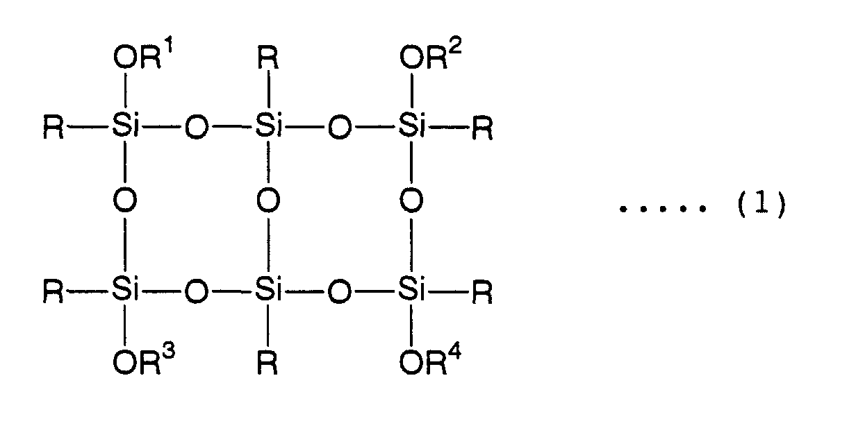
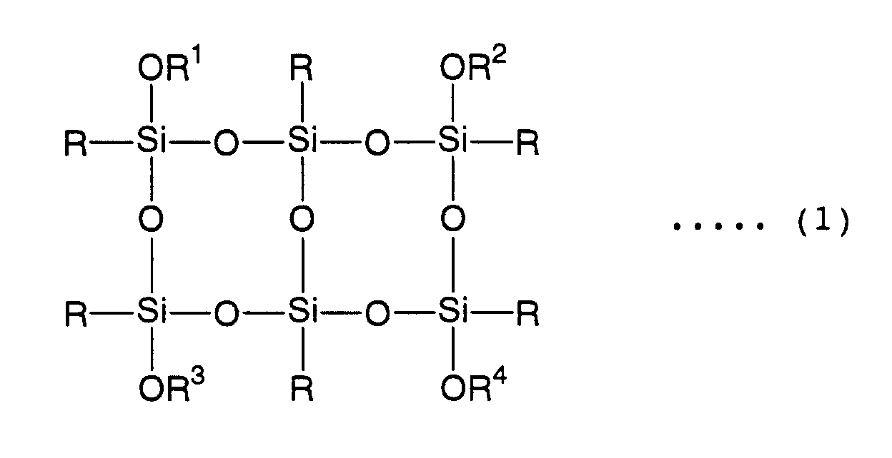
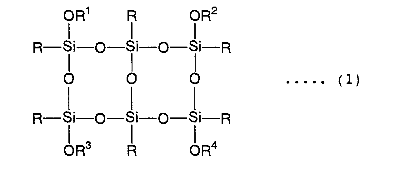
- the present invention provides a photo-curable resin composition capable of undergoing polymerization and curing upon absorption of actinic ray, at least one portion of the resin composition comprising an organic silicic compound represented by the following formula (1) or (2): where R is an organic group reacting with an epoxy group; and R 1 to R 6 are independently silicon-containing groups having 0-3 repeat units of (SiRO 3/2 ); in case the unit of (SiRO 3/2 ) is zero, R 1 to R 6 are independently H, CH 3 or C 2 H 6 , an epoxy resin and a photo initiator capable of initiating polymerization of the organic silicic compound or the epoxy resin upon absorption of actinic ray, and a process for producing the same.
- R is an organic group reacting with an epoxy group
- R 1 to R 6 are independently silicon-containing groups having 0-3 repeat units of (SiRO 3/2 ); in case the unit of (SiRO 3/2 ) is zero, R 1 to R 6 are independently H, CH 3 or C 2 H 6 , an epoxy
- the present invention also provides products using the resin composition, e.g., multilayered wiring boards and semiconductor devices.
- Figs. 1A-1G are cross-sectional views showing a flow of process steps for producing a wiring board according to Example 8.
- Fig. 2 is a cross-sectional view showing a wiring board according to Example 8.
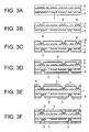
- Figs. 3A-3F are cross-sectional views showing a flow of process steps for producing a wiring board according to Example 9.
- Fig. 4 is a cross-sectional view showing a wiring board according to Example 9.
- Fig. 5 is a cross-sectional view showing a semiconductor device according to Example 9.
- Figs. 6A-6H are cross-sectional views showing a flow of process steps for producing a semiconductor device according to Example 10.
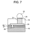
- Fig. 7 is an enlarged cross-sectional view showing a semiconductor device of Fig. 6H.
- the present photo-curable resin composition is a resin composition capable of undergoing polymerization and curing upon absorption of actinic ray, at least a portion of the resin composition comprising an organic silicic compound represented by the following formula (1) or (2): where R is an organic group reacting with an epoxy group; and R 1 to R 6 are independently silicon-containing groups having 0-3 repeat units of (SiRO 3/2 ); in case the unit (SiRO 3/2 ) is zero, R 1 to R 6 are independently H, CH 3 or C 2 H 6 , an epoxy resin and a photo initiator capable of initiating polymerization of the organic silicic compound or the epoxy resin upon absorption of actinic ray.
- R is an organic group reacting with an epoxy group
- R 1 to R 6 are independently silicon-containing groups having 0-3 repeat units of (SiRO 3/2 ); in case the unit (SiRO 3/2 ) is zero, R 1 to R 6 are independently H, CH 3 or C 2 H 6 , an epoxy resin and a photo initiator capable of
- any well known epoxy resin can be used without any particular restriction and includes, for example, bisphenol A type epoxy resin, bisphenol F type epoxy resin, novolak type epoxy resin, o-cresol novolak epoxy resin, m-cresol novolak type epoxy resin, alycidylamine type epoxy resin, alicyclic epoxy resin, etc.
- fluorine-containing epoxy resin and fluorine-containing acrylic resin can be effectively used.
- Epoxy acrylate resin or epoxy methacrylate resin obtained by acrylating or methacrylating portions of epoxy groups of the aforementioned epoxy resins by addition of propenoyl chloride or 2-methylpropenoyl chloride thereto can be also used.
- the aforementioned epoxy resins can be used alone or in mixture of at least two thereof.
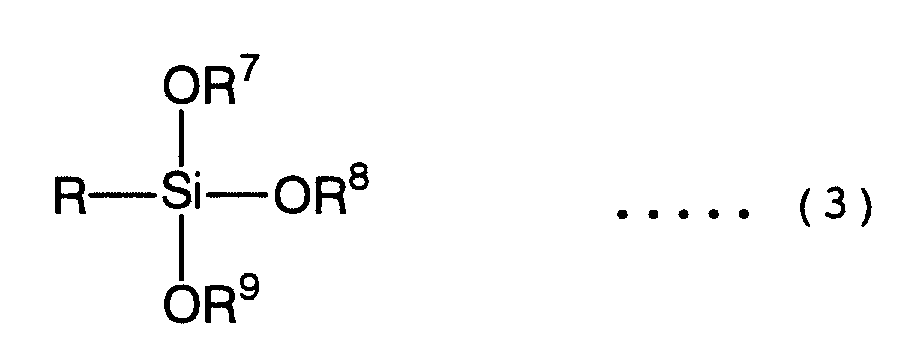
- the present photo-curable resin composition can be produced by a process comprising a step of heat treating a mixture comprising an epoxy resin, an organic silicic compound represented by the following formula (3): where R is an organic group reacting with either the aforementioned epoxy group or vinyl group; and R 1 is CH 3 or C 2 H 5 , and water at a temperature of preferably 60° - 160°C for 1-10 hours and a step of mixing a photo initiator with the heat-treated mixture.
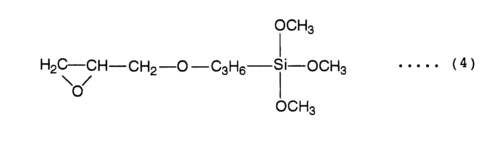
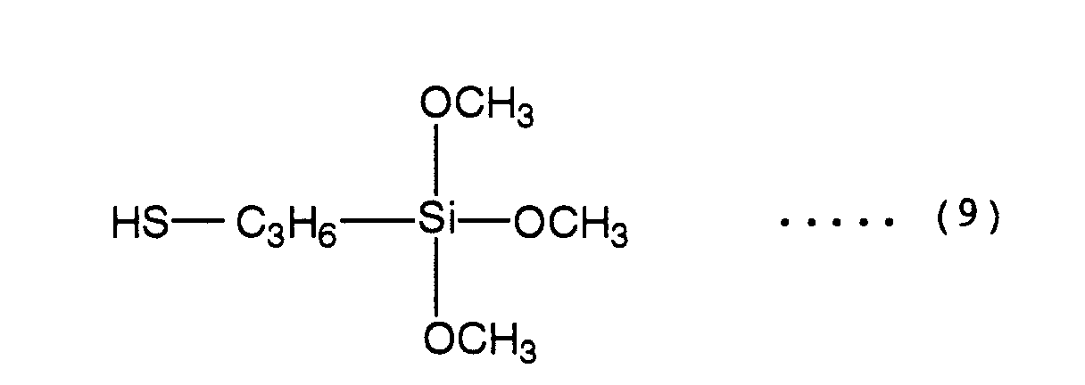
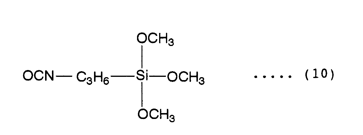
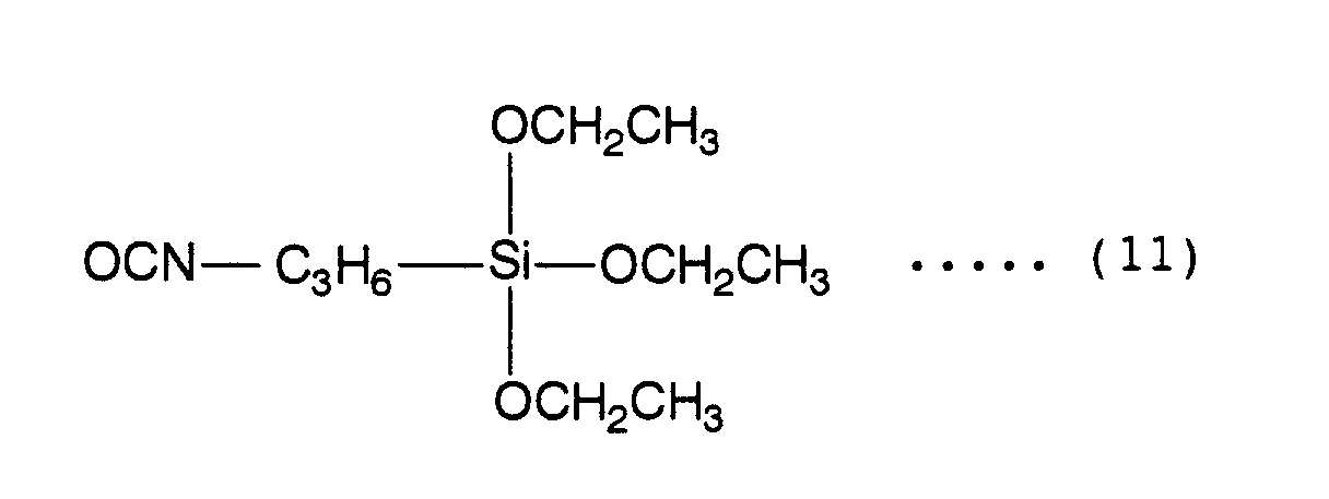
- Organic silicic compound represented by the foregoing formula (3) for use in the present invention includes, for example, organic silicic compounds having functional groups represented by the following formulae (4)-(11):
- the organic silicic compound is not restricted to those as mentioned above and can be used alone or in combination at least two thereof.
- a photo initiator capable of generating an acid or both radical and acid can be used upon proper selection in view of functional groups contained in the matrix resin or organic groups of organic silicic compound.
- Acid generator includes onium salts such as diazonium salts, sulfonium salts, iodonium salts, etc. represented by ArN 2 + Z - , (R) 3 S + Z - , (R) 2 I + Z - , etc. (where Ar is an aryl group; R is an aryl group or an alkyl group having 1-20 carbon atoms; and Z - is an anion, e.g.
- organo-metallic compounds or the like specifically includes triallylsulfonium hexafluorophosphate, bis(4-diphenylsulfoniophenyl)sulfonium bishexafluorophosphate, (4-phenylthiophenyl)diphenylsulfonium hexafluorophosphate, p-benzoyldiphenyliodonium hexafluorophosphate, (4-methoxyphenyl)diphenylsulfonium hexafluoroautimonate, (4-methoxyphenyl)phenyliodonium hexafluoroantimonate, (2,4-cyclopentadiene-1-yl)[(1-methylethyl)benzene]-Fe-hexafluorophosphate, etc., but is not limited there
- sulfonium salts and p-benzoyldiphenyliodonium hexafluorophosphate belonging to he aforementioned acid generator are known.
- the present photo-curable resin composition can be admixed with well known curing agents, curing accelerators, cross-linking agents, mold-releasing agents, defoaming agents, coupling agents, sensitizer, diluents, flame retardants, solvents, etc., depending on the purpose and uses.
- Cured products obtained from the photo-curable resin composition of the present invention show the following physical properties at 200°C to 225°C (Tg + 40°C):
- Products obtained by using the present photo-curable resin composition include, for example, multilayered wiring boards and semiconductor devices.
- Multilayered wiring board comprises conductor layers, insulating layers composed of photo-curable resin composition and formed between the conductor layers and a filler filled in blind via holes interconnecting the conductor layers one to another, where at least one of the insulating layers is formed from a photo-curable resin composition, which comprises an organic silicic compound represented by the following general formula (1) or (2): (where R is an organic group reacting with an epoxy group and R 1 to R 6 are silicon-containing groups having 0-3 repeat units of (SiRO 3/2 ); in case the unit of (SiRO 3/2 ) is zero, R 1 to R 6 are independently H, CH 3 or C 2 H 6 ), an epoxy resin and a photo initiator capable of initiating polymerization of the organic silicic compound or the epoxy resin upon absorption of actinic ray.
- a photo-curable resin composition which comprises an organic silicic compound represented by the following general formula (1) or (2): (where R is an organic group reacting with an epoxy group and R 1 to R 6 are silicon-containing groups having 0
- Semiconductor device comprises a semiconductor component having projected electrodes on the surface, a resin composition covering the projected electrodes and ball electrodes connected to the projected electrodes exposed from the resin composition, where the resin composition is a photo-curable resin composition, which comprises an organic silicic compound represented by the following general formula (1) or (2): (where R is an organic group reacting with an epoxy group and R 1 to R 6 are silicon-containing groups having 0-3 repeat units of (SiRO 3/2 ); in case the unit of (SiRO 3/2 ) is zero, R 1 to R 6 are independently H, CH 3 or CH 2 CH 3 ), an epoxy resin and a photo initiator capable of initiating polymerization of the organic silicic compound or the epoxy resin upon absorption of actinic ray.
- a photo-curable resin composition which comprises an organic silicic compound represented by the following general formula (1) or (2): (where R is an organic group reacting with an epoxy group and R 1 to R 6 are silicon-containing groups having 0-3 repeat units of (SiRO 3/2 ); in case
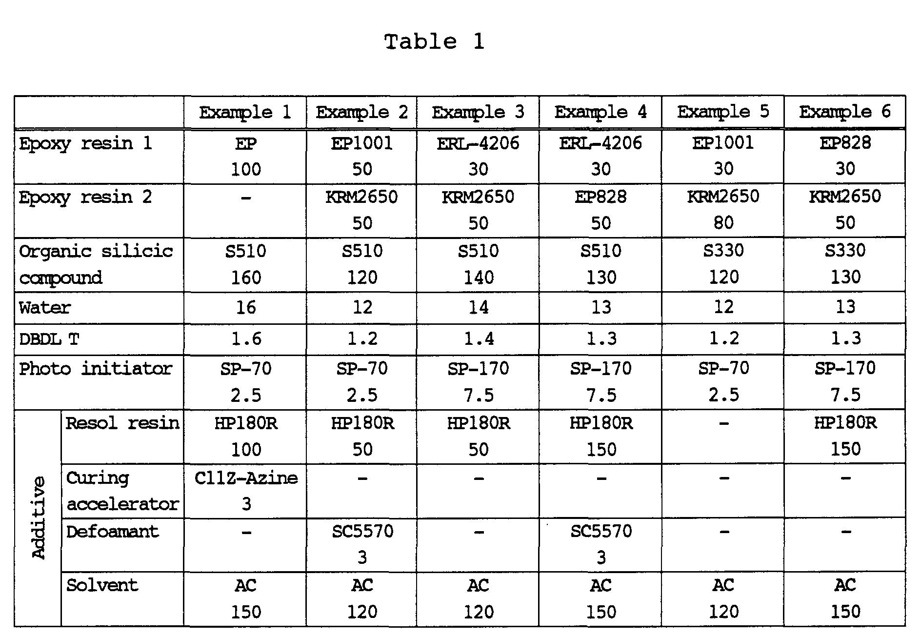
- a photo-curable resin composition (in grams) according to Example 1 is shown, where 3-glycidoxytrimethoxysilane (S510, made by Chisso Corp.) was used as an organic silicic compound, tin dibutyldilaurate (DBDL T, made by Wako Pure Chemical Industries, Ltd.) as a hydrolysis catalyst, bisphenol A type epoxy resin (EP1001, made by Yuka Shell Co., Ltd.) as an epoxy resin, triallylsulfonium hexafluorophosphate type photo initiator (SP-70, made by Asahi Denka Kogyo K.K.), and resol resin (HP180R, made by Hitachi Chemical Co., Ltd.), imidazole (C11Z-Azine, made by Shikoku Chemical Corp.) and 1-acetoxy-2-methoxyethane (AC, made by Wako Pure Chemical Industries, Ltd.) as additives.
- S510 3-glycidoxytrimethoxysilane
- the composition thus prepared was applied to a copper foil by an applicator and heated at 80°C for 30 minutes for drying, thereby obtaining a 50 ⁇ m-thick resin layer.
- the resin layer After irradiation of ultraviolet ray at 1,500 mJ/cm 2 by a high pressure mercury lamp, the resin layer is heated at 150°C for 15 minutes and then at 140°C for 30 minutes for curing. Then, the copper foil was dissolved off to obtain a cured product.
- the resulting cured resin product was tested according to the following procedures to determine Tg, changes in modulus of elasticity by temperature and bonding strength to the copper foil.
- the cured product thus obtained was cut into a test piece, 25 mm ⁇ 4 mm, and the test piece was tested to determine changes in dynamic (storage) modulus of elasticity by temperature by a rheospectrometer (model DVE4, made by Rheology Co., Ltd.) under the following conditions:
- a tan ⁇ peak was presumed to be a glass transition temperature (Tg) and dynamic (storage) moduli of elasticity at room temperature (25°C) and a higher temperature by 40°C than Tg, respectively, were determined.
- the cured product thus obtained was cut into a test piece, 20 mm ⁇ 4 mm, and the test piece was tested to determine changes in the length of test piece by a TMA tester (made by Shinku Rikou Co., Ltd.) under the following conditions:
- Coefficient of thermal expansion was determined from changes in the length of test piece between room temperature (25°C) and a higher temperature by 40°C than Tg.
- the photo-curable resin composition was applied to the mat surface of a 18 ⁇ m-thick copper foil and dried to make the dried 75 ⁇ m-thick resin layer.
- the resin-lined copper foil was then pressure bonded to a 5 mm-thick glass substrate by a laminator and then subjected to irradiation of ultraviolet ray from the glass substrate side in the same manner as in case of preparing the cured product and then to the similar heat treatments for curing.
- the copper foil was etched into 10 mm-wide test pieces, and the test pieces were peeled off at an angle of 90° at room temperature and a higher temperature by 40°C than Tg, respectively, to determine the bonding strength of the cured product to the copper foil test pieces. The bonding strength was presumed to be a peel strength.
- Copper foil surfaces of a laminate board lined with 18 ⁇ m-thick copper foils on both sides were treated with a surface-roughening solution (containing 7 ml/l of sulfuric acid and 180 g/l of ammonium persulfate) at 30°C for 2 minutes to make finely uneven surfaces.
- composition prepared according to Example 1 was applied to the copper foils by an applicator, heated at 80°C for 30 minutes and dried to obtain 50 ⁇ m-thick resin layers, the resin layers were irradiated with ultraviolet ray from a high pressure mercury lamp in the same manner as above through a mask printed with circular holes having hole diameters of 10-250 ⁇ m, the hole diameters being different from one to another at every interhole distance of 10 ⁇ m.
- aqueous 0.8 wt.% borax solution comprising 100 ml of 2-butoxyethanol, 100 ml of pure water, and 100 ml of an aqueous 15% tetramethylammonium hydroxide solution (the developing solution will be hereinafter referred to as "quasi-aqueous developing solution").
- the irradiated resin layers were developed by spraying with the quasi-aqueous developing solution at 30°C for 1.5 minutes, then washed with water for 3 minutes and dried by injection of dry air. After the drying, holes thus formed were observed by an optical microscope or SEM, and the smallest diameter among the diameters of via holes formed by development was presumed to be "resolution".
- Pulverized cured product was subjected to 29 Si-NMR measurement by FT-NMR (model JNM-GSZ400, made by JEOL Ltd.) to determine chemical shift peak position and its integration value.
- a ratio of peak integration value at -53 ppm to -75 ppm to that at -40 ppm to -52 ppm was obtained.
- Example 1 Example 2 Example 3 Example 4 Example 5
- Example 6 Dynamic viscoelasticity Tg (°C) 180 185 180 185 160 175 Storage modulus of elasticity (25°C) (GPa) 2.0 1.9 2.2 1.9 1.8 1.8 Storage modulus of elasticity (Tg+40°C) (GPa) 0.45 0.4 0.5 0.55 0.4 0.4 Bonding strength (kN/m) Room temp. 1.5 1.5 1.3 1.3 1.4 1.4 Tg+40°C 0.8 0.9 0.8 0.7 0.8 0.8 Resolution ( ⁇ m) 40 50 50 30 50 50 50 Si-NMR results 6.9 5.2 6.8 7.5 5.2 8.5
- Photo-curable resin composition (in grams) according to Example 2 is shown in Table 1, where 3-glycidoxytrimethoxysilane (S510, made by Chisso Corp.) was used as an organic silicic compound, tin dibutyldilaurate (DBDL T, made by Wako Pure Chemical Industries, Ltd.) as a hydrolysis catalyst, bisphenol A type epoxy resin (EP1001, made by Yuka Shell Co., Ltd.) and o-cresol novolak type epoxy resin (KRM2650, made by Asahi Denka Kogyo K.K.) as epoxy resins, triallylsulfonium hexafluorophosphate type photo initiator (SP-70, made by Asahi Denka Kogyo K.K.), and resol resin (HP180R, made by Hitachi Chemical Co., Ltd.) a defoamant (SC5570, made by Toray Silicone Co., Ltd.) and 1-acetoxy-2-methoxyethane (AC
- Photo-curable resin composition (in grams) according to Example 3 is shown in Table 1, where 3-glycidoxytrimethoxysilane (S510, made by Chisso Corp.) was used as an organic silicic compound, tin dibutyldilaurate (DBDL T, made by Wako Pure Chemical Industries, Ltd.) as a hydrolysis catalyst, alicyclic epoxy resin (ERL-4206, made by Union Carbide Corp.) and o-cresol novolak epoxy resin (KRM2650, made by Asahi Denko K.K.) as epoxy resins, triallylsulfonium hexafluorophosphate type photo initiator (SP-170, made by Asahi Denka Kogyo K.K.), and resol resin (HP180R, made by Hitachi Chemical Co., Ltd.) and 1-acetoxy-2-methoxyethane (AC, made by Wako Pure Chemical Industries, Ltd.) as additives.
- S510 3-glycidoxytrimeth
- Example 2 preparation of cured product and evaluation of characteristics were also carried out in the same manner as in Example 1, and the results are shown in Table 2.
- Photo-curable resin composition (in grams) according to Example 4 is shown in Table 1, where 3-glycidoxytrimethoxysilane (S510, made by Chisso Corp.) was used as an organic silicic compound, tin dibutyldilaurate (DBDL T, made by Wako Pure Chemical Industries, Ltd.) as a hydrolysis catalyst, alicyclic epoxy resin (ERL-4206, made by Union Carbide Corp.) and bisphenol A type epoxy resin (EP828, made by Yuka Shell Co., Ltd.) as epoxy resins, and triallylsulfonium hexafluorophosphate type photo initiator (SP170, made by Asahi Denka K.K.), and furthermore, resol resin (HP180R, made by Hitachi Chemical Co., Ltd.) a defoamant (SC5570, made by Toray Silicone Co., Ltd.) and 1-acetoxy-2-methoxyethane (AC, made by Wako Pure Chemical Industries, Ltd.)
- Example 2 preparation of cured product and evaluation of characteristics were also carried out in the same manner as in Example 1, and the results are shown in Table 2.
- Photo-curable resin composition (in grams) according to Example 5 is shown in Table 1, where 3-aminopropyltriethoxysilane (S330, made by Chisso Corp.) was used as an organic silicic compound, tin dibutyldilaurate (DBDL T, made by Wako Pure Chemical Industries, Ltd.) as a hydrolysis catalyst, bisphenol A type epoxy resin (EP1001, made by Yuka Shell Co., Ltd.) and o-cresol novolak type epoxy resin (KRM2650, made by Asahi Denka Kogyo K.K.) as curable epoxy resins, triallylsulfonium hexafluorophosphate (SP-70, made by Asahi Denka Kogyo K.K.) as a photo initiator, and 1-acetoxy-2-methoxyethane (AC, made by Wako Pure Chemical Industries, Ltd.) as an additive.
- S330 3-aminopropyltriethoxysilane
- Photo-curable resin composition (in grams) according to Example 6 is shown in Table 1, where 3-aminopropyltriethoxysilane (S330, made by Chisso Corp.) was used as an organic silicic compound, tin dibutyldilaurate (DBDL T, made by Wako Pure Chemical Industries, Ltd.) as a hydrolysis catalyst, alicyclic epoxy resin (ERL-4206, made by Union Carbide Corp.) and bisphenol A type epoxy resin (EP828, made by Yuka Shell Co., Ltd.) as epoxy resins, and triallylsulfonium hexafluorophosphate type photo initiator (SP-170, made by Asahi Denka Kogyo K.K.). Furthermore, resol resin (HP180R, made by Hitachi Chemical Co., Ltd.) and 1-acetoxy-2-methoxyethane (AC, made by Wako Pure Chemical Industries, Ltd.) were used as additives.
- S330 3-aminopropyltrieth
- Photo-curable resin composition (in grams) according to Comparative Example 1 is shown in Table 3, where bisphenol A type epoxy resin (EP1001, made by Yuka Shell Co., Ltd.) was used as curable resin, triallylsulfonium hexafluorophosphate type photo initiator (SP-70, made by Asahi Denka Kogyo K.K.), and resol resin (HP180R, made by Hitachi Chemical Co., Ltd.) and 1-acetoxy-2-methoxyethane (AC, made by Wako Pure Chemical Industries, Ltd.) as additives.
- PC-70 triallylsulfonium hexafluorophosphate type photo initiator
- HP180R made by Hitachi Chemical Co., Ltd.
- AC 1-acetoxy-2-methoxyethane
- Photo-curable resin composition (in grams) according to Comparative Example 2 is shown in Table 3, where bisphenol A type epoxy resin (EP1001, made by Yuka Shell Co., Ltd.) was used as a curable resin, triallylsulfonium hexafluorophosphate type photo initiator (SP-70, made by Asahi Denka Kogyo K.K.), and resol resin (HP180R, made by Hitachi Chemical Co., Ltd.), 1-acetoxy-2-methoxyethan (AC, made by Wako Pure Chemical Industries, Ltd.) and a silica filler having an average particle size of 1 ⁇ m (Crystalite 5Z, made by Tatsumori K.K.) as additives.
- EP1001 made by Yuka Shell Co., Ltd.
- SP-70 triallylsulfonium hexafluorophosphate type photo initiator
- HP180R made by Hitachi Chemical Co., Ltd.
- AC 1-acetoxy-2-methoxyethan
- Photo-curable resin composition (in grams) according to Comparative Example 3 is shown in Table 3, where bisphenol A type epoxy resin (EP1001, made by Yuka Shell Co., Ltd.) and o-cresol novolak type epoxy resin (KRM2650, made by Asahi Denka Kogyo K.K.) were used as curable resins, triallylsulfonium hexafluorophosphate type photo initiator (SP-70, made by Asahi Denka Kogyo K.K.), and resol resin (HP180R, made by Hitachi Chemical Co., Ltd.) and 1-acetoxy-2-methoxy-ethane (AC, made by Wako Pure Chemical Industries, Ltd.) as additives.
- EP1001 made by Yuka Shell Co., Ltd.
- KRM2650 o-cresol novolak type epoxy resin
- SP-70 triallylsulfonium hexafluorophosphate type photo initiator
- HP180R made by Hitachi Chemical Co.,
- Photo-curable resin composition (in grams) according to Comparative Example 4 is shown in Table 3, where the resin composition was prepared in the same manner as in Comparative Example 3, except that 21 g of Crystalite 5Z was used, and the resin composition was kneaded through three rolls to uniformly disperse Crystalite 5Z, thereby obtaining a final photo-curable resin composition. Preparation of cured product and evaluation of characteristics were carried out in the same manner as in Comparative Example 1. The results are shown in Table 4.
- Photo-curable resin composition (in grams) according to Comparative Example 5 is shown in Table 3, where 3-glycidoxytrimethoxysilane (S510, made by Chisso Corp.) was used as an organic silicic compound, Tin dibutyldilaurate (DBDL T, made by Wako Pure Chemical Industries, Ltd.) as a hydrolysis catalyst, bisphenol A type epoxy resin (EP1001, made by Yuka Shell Co., Ltd.) and o-cresol novolak type epoxy resin (KRM2650, made by Asahi Denka Kogyo K.K.) as curable resins, triallylsulfonium hexafluorophosphate type photo initiator (SP-70, made by Asahi Denka Kogyo K.K.), and resol resin (HP180R, made by Hitachi Chemical Co., Ltd.) and 1-acetoxy-2-methoxyethane (AC, made by Wako Pure Chemical Industries, Ltd.) as additives.
- S510 3-g
- Characteristics of cured products of Examples 1 to 6 are shown in Table 2, where decreases in the storage modulus of elasticity and the bonding strength from room temperature to 220°C, which is higher than the glass transition temperatures, can be controlled within about 1/5, and also resolution is in a range of 60-30 ⁇ m, which can be evaluated as a high resolution.
- Comparative Example 1 corresponds to Example 1, except that no organic silicic compound of Example 1 is used, and shows large differences in the storage modulus of elasticity between room temperature higher temperature than Tg and considerable changes in the physical properties at higher temperatures than Tg.
- the bonding strength at higher temperatures becomes very low, as compared with that at room temperature, and when applied to different kinds of materials as an adhesive, peeling of the adhesive will often take place due to developed thermal stresses.
- Comparative Example 2 shows the same resin composition as that of Example 1, except that a silica filler is used in place of the organic silicic compound of Example 1.
- Comparative Example 2 contains substantially the same O-Si-O skeleton component as in Example 1 in the form of a filler, and thus the storage modulus of elasticity at higher temperatures than Tg is improved, but the bonding strength at higher temperatures is not improved and resolution is lowered due to light scattering by the filler.
- Comparative Example 3 corresponds to Example 2, except that no organic silicic compound is used, and shows large differences in the storage modulus of elasticity between room temperature and higher temperatures than Tg and considerable changes in the physical properties at higher temperatures than Tg, as in Comparative Example 1.
- Comparative Example 4 shows the same resin composition as that of Example 2, except that a silica filler is used in place of the organic silicic compound of Example 2. No improvement of the bonding strength is observed and lowering of resolution is observed, as in Comparative Example 2.
- Comparative Example 5 uses an organic silicic compound, but the curable resin composition of Comparative Example 5 is prepared without heat treatment of the organic silicic compound in the curable resin in contrast to the present invention. NMR measurement results show that polymerization of the organic silicic compound fails to proceed. That is, in spite of the fact that the same amount of the organic silicic compound as in Example 2 is used as a starting material, it has been found that changes in the storage modulus of elasticity between room temperature and higher temperatures than Tg are the same as in Comparative Example 3 using no organic silicic compound, and the physical properties are considerably changed between room temperature and higher temperatures than Tg.
- the cured products show at 200° to 225°C the storage modulus of elasticity of 0.4 to 0.55 GPa and the bonding strength of 0.7 to 0.9 kN/m, respectively. These values have differences of -1.25 to -1.89 GPa and -0.4 to -0.8 kN/m, respectively, compared with the values at room temperature (25°C). Comparing with the same differences in the values in Comparative Examples 1 to 5, that is, -2.8 to -3.3 GPa in the storage modulus of elasticity and -1.0 to -1.4 kN/m in the bonding strength, the above-mentioned values in the present invention are clearly smaller in the absolute value. As a result, it can be said that the storage modulus of elasticity and the bonding strength of cured products according to the present invention are maintained at high temperatures higher than Tg.
- a photo-curable resin composition effective for photo-curable insulating layers on electronic parts including build-up type multilayered wiring boards, capable of producing cured products with less light scattering, distinguished resolution, and small decrease in physical properties at higher temperatures than the glass transition temperature, can be obtained according to the present invention.
- Resin composition was prepared in the same manner as in Example 2, except that heat treatment was carried out under changed conditions after addition of a liquid mixture of S510, water and DBDL T to EP1001 and KRM2650, followed by uniform mixing. Temperature and time used for the heat treatment were 60°C for one hour and 60°C for 10 hours; 80°C for 4 hours; 160°C for one hour; and 160°C for 4 hours. Preparation of cured products and evaluation of characteristics were carried out in the same manner as in Example 1. The results are shown in Table 5. Comp. Ex. 6 Comp. Ex. 7 Comp. Ex. 8 Example 7 Heat treatment conditions 50°C-1 hr. 50°C-10 hr. 150°C-0.5 hr. 60°C-1 hr. 60°C-10 hr.
- Resin compositions were prepared in the same manner as in Example 2, except that heat treatment was carried out unde changed conditions after addition of a liquid mixture of S510, water and DBDL T to EP1001 and KRM2650, followed by uniform mixing. Temperature and time used for the heat treatment were 50°C for one hour (Comparative Example 6), 50°C for 10 hours (Comparative Example 7), 150°C for 0.5 hours (Comparative Example 8) and 170°C for one hour (Comparative Example 9), but in case of 170°C for one hour of Comparative Example 9, the liquid mixture underwent gelling, resulting in failure to evaluate the characteristics. Preparation of cured products and evaluation of characteristics were carried out in the same manner as in Example 1. The results are shown in Table 5.
- a multilayered wiring board with blind via holes was prepared in the following manner, using the afore-mentioned photo-curable resin composition and its characteristics as a semiconductor package were evaluated.
- Figs. 1A-1G are schematic view showing a flow of process steps of preparing a six-layered wiring board.
- Laminate board 1 lined with 18 ⁇ m-thick copper foils of ultraviolet ray-nontransmissible type on both sides (NCL-67Nw, made by Hitachi Chemical Co., Ltd.) was used and inner layer power source circuit 2 was formed thereon by predetermined etching. Copper foil surface of the circuit was treated with a roughening solution containing 7 ml/l of sulfuric acid and 180 g/l of ammonium persulfate at 30°C for 2 minutes to make a finely uneven surface.
- the finely uneven surface was treated with an oxide film-forming solution containing 35 g/l of trisodium phosphate, 100 g/l of sodium perchlorate and 10 g/l of sodium hydroxide at 70°C for 5 minutes to form an oxide film in an ultramicrogranular state on the finely uneven surface.
- the oxide film was treated with a reducing solution containing 10 g/l of dimethylamineborane and 7 g/l of sodium hydrode at 40°C for 2 minutes to reduce the oxide film.
- water was removed by nitrogen gas injection to dry the surface.
- Photo-curable resin composition 3 of Example 2 was applied to one side of the inner layer circuit board by screen printing, heated at 60°C for 20 minutes and dried.
- the resin composition was also applied to the other side in the same manner as above, heated at 60°C for 30 minutes and dried, where the resin layers were each made to have a thickness of 50 ⁇ m.
- Both layers were then irradiated with parallel ultraviolet ray of a high pressure mercury lamp at 1,500 mJ/cm 2 through masks printed with via holes, 50 ⁇ m in diameter, at predetermined positions, and then developed with an aqueous 1 wt.% sodium carbonate solution at 30°C for 150 seconds by spraying, followed by further irradiation at 1 J/cm 2 and heating at 150°C for one hour.
- Photo-curable resin composition surface 3 on the board was roughened with a chemical roughening solution containing 80 g/l of potassium permanganate, whose pH was adjusted to 13 by potassium hydroxide, at 50°C for 5 minutes and washed with water, followed by hot water washing at 50°C for 5 minutes. Then, the roughening residue was removed with an aqueous 6 g/l sodium hydroxide solution.
- the surface was further washed with water, and then the board was dipped into a catalyst solution containing palladium acting as a catalyst for electroless plating (chemical plating) reaction (HS101B, made by Hitachi Chemical Co., Ltd.) and again washed with water, followed by activation of the catalyst with an aqueous 100 ml/l hydrochloric acid solution.
- a catalyst solution containing palladium acting as a catalyst for electroless plating (chemical plating) reaction (HS101B, made by Hitachi Chemical Co., Ltd.
- the board was dipped into an electroless copper plating solution containing 10 g/l of copper sulfate, 30 g/l of ethylenediaminetetraacetic acid, 3 ml/l of an aqueous 37% HCHO solution and 30 mg/l of ⁇ , ⁇ '-dipyridyl, whose pH was adjusted to 12.5 by sodium hydroxide, at 70°C for 10 minutes to form copper plating films 5, about 30 ⁇ m thick, thick, in blind via holes 4 and wiring board surfaces.
- the copper plating films were washed with water and then heat treated at 160°C for 30 minutes.
- Etching resist was provided on the copper plating, and then the copper was etched to form a circuit.
- the foregoing procedures were successively repeated to form two inner layer circuits on each side and finally throughholes 6 and an outemost circuit layer were formed. It was confirmed that through the foregoing process steps, a multilayered wiring board, 27 mm ⁇ 27 mm, was finally prepared without any problems.
- numeral 7 shows a build-up type multilayered wiring board.
- Filler resin 13 (CCT-65TH, made by Asahi Research Laboratory Co., Ltd.) was filled into the throughholes of the wiring board by screen printing and cured at 170°C for one hour. Then, as shown in Fig. 2, solder resist 12 and gold plating 9 were provided at desired positions, where insulating layers 3 were 45 ⁇ m thick. Die bonding paste (EN-4000, made by Hitachi Chemical Co., Ltd.) was potted in an area, 7 mm ⁇ 7 mm, by a dispenser, and semiconductor chip 11, 7 mm ⁇ 7 mm, was provisionally bonded thereto at 180° for one minute under a load of 5 kg/cm 2 . Then, the paste was cured at 180°C for one hour. In Fig. 2, numeral 8 shows copper wirings.
- wire bonding was carried out between the bonding parts and semiconductor chip 11 on the printed wiring board, using gold wire 10, 30 ⁇ m in diameter, by a manual bonding apparatus. Bonding conditions were as follows:
- Figs. 3A-3F are schematic views showing a flow of process steps of preparing a five-layered wiring board
- Fig, 4 is a cross-sectional view of the five-layered wiring board thus prepared.
- the finely uneven surface was treated with an oxide film-forming solution containing 35 g/l of trisodium phosphate, 100 g/l of sodium perchlorate and 10 g/l of sodium hydroxide at 70°C for 5 minutes to form an oxide film in an ultramicrogranular state on the finely uneven surface.
- the oxide film was treated with a reducing solution containing 10 g/l of dimethylamineborane and 7 g/l of sodium hydroxide at 40°C for 2 minutes to reduce the oxide film.
- water was removed by nitrogen gas injection to dry the surface.
- Both sides of the inner layer circuit board was dipped into a catalyst solution containing palladium acting as catalyst 8 for electroless plating (chemical plating) (HS101B, made by Hitachi Chemical Co., Ltd.) for 2 minutes and dried. Then, photo-curable resin composition 3 of Example 2 was applied to one side of the circuit board by screen printing, heated at 60°C for 20 minutes, and dried. The resin composition was also applied to the other side in the same manner as above, heated at 60°C for 30 minutes and dried, where the resin layers were each made to have a thickness of 50 ⁇ m.
- HS101B electroless plating
- Both layers were then irradiated with parallel ultraviolet ray of a high pressure mercury lamp at 400 mJ/cm 2 through masks printed with via holes, 50 ⁇ m in diameter, at predetermined positions, and then developed with an aqueous 1 wt.% sodium carbonate solution at 30°C for 150 seconds, followed by further irradiation at 1 J/cm 2 and heating at 150°C for one hour.
- catalyst 8 was activated with an aqueous 100 ml/l hydrochloric acid solution.
- the wiring board was dipped into an electroless copper plating solution containing 10 g/l of copper sulfate, 30 g/l of ethylenediaminetetraacetic acid, 3 ml/l of an aqueous 37% HCHO solution and 30 mg/l of ⁇ , ⁇ '-dipyridyl, whose pH was adjusted to 12.5 by sodium hydroxide, at 70°C for ten hours to form copper plating films, about 30 ⁇ m thick, in blind via holes 4 and on the surfaces of the wiring board.
- the wiring board was washed with water and heat treated at 160°C for 30 minutes.
- Fig. 5 is a cross-sectional view showing a multilayered printed wiring board, 27 mm ⁇ 27 mm, prepared according to the foregoing procedures.
- filler resin 13 was filled and cured in the same manner as in Example 8, and solder resists 12 and gold platings 9 were provided at predetermined positions.
- Underfill 14 (LPD197, made by Japan Locktight Co., Ltd.) was filled between the semiconductor chip and the wiring board and heat cured at 150°C for 12 hours.
- Example 8 The foregoing package was subjected to a temperature cycle test in the same manner as in Example 8. No abnormality of electric signals was found at 3,000 cycles or more in this Example.
- the package was subjected to a temperature cycle test in the same manner as in Example 8 and abnormality of electric signals was found at 1,000 cycles in this Comparative Example.
- Figs. 6A-6H are cross-sectional views showing a flow of process steps for producing a CSP semiconductor device, using the present photo-curable resin composition
- Fig. 7 is a partly enlarged cross-sectional view of CSP21 in Fig. 6H.
- the resin composition was heated at 120°C for 15 minutes and then non-irradiated parts were removed by a developing solution, followed by conducting curing reaction at 140°C for 30 minutes and 180°C for 180 minutes in the same manner as in Example 2, thereby obtaining the wafer with an arrangement of vias 20 as shown in Fig. 6D.
- copper posts 21 were formed by electrolytic copper plating (Fig. 6E), and barrier metals, not shown here (but 25 in Fig. 7) were formed by Ni plating, and solder balls 22 were formed thereon (Fig. 6F).
- Fig. 6G chips were divided one from another by diamond blade 23 to form chip size packages.
- CSP (chip size package) 24 as shown in Fig. 6H was finally obtained.
- CSP of wafer size can be prepared without removal of plating resist, filling of sealing resin and grinding of sealing resin, resulting in material cost reduction and process simplification.
- a package was prepared from CSP thus prepared and the wiring board of Example 9 in the same manner as in Example 9, and subjected to a temperature cycle test in the same manner as in Example 8. No abnormality of electric signals was found at 3,000 cycles in this Example.
- numeral 26 shows polyimide, 27 SiN, 28 Al electrode and 29 wiring layer.
- CSP was prepared in the same manner as in Example 12, except that photo-curable resin of Comparative Example 2 was used.
- a package was prepared from CSP thus prepared and the wiring board of Example 9 in the same manner as in Example 9 and subjected to a temperature cycle test in the same manner as in Example 8. It was found that electric signals were no more conducted at 300 cycles.
- cured products of the present photo-curable resin composition can maintain a desired modulus of elasticity at temperatures as high as or higher than Tg witghout any decrease in the bonding strength at elevated temperatures and without any decrease in resolution due to light scattering because of uniform distribution at the molecular level of organic silicic compound having thermodynamically stable Si-O-Si bonds.
- the present photo-curable resin composition is applicable to printed wiring boards or CSPs requiring fine pattern formation without any development of inconveniences such as cracks, peeling, etc., contributing to considerable improvement of reliability of electronic appliances using the wiring boards at CSPs.
Landscapes
- Chemical & Material Sciences (AREA)
- Health & Medical Sciences (AREA)
- Chemical Kinetics & Catalysis (AREA)
- Medicinal Chemistry (AREA)
- Polymers & Plastics (AREA)
- Organic Chemistry (AREA)
- Physics & Mathematics (AREA)
- General Chemical & Material Sciences (AREA)
- Emergency Medicine (AREA)
- Spectroscopy & Molecular Physics (AREA)
- General Physics & Mathematics (AREA)
- Epoxy Resins (AREA)
- Compositions Of Macromolecular Compounds (AREA)
- Adhesives Or Adhesive Processes (AREA)
- Materials For Photolithography (AREA)
- Silicon Polymers (AREA)
- Organic Insulating Materials (AREA)
Abstract
Description








| Example 1 | Example 2 | Example 3 | Example 4 | Example 5 | Example 6 | ||
| Dynamic viscoelasticity | Tg (°C) | 180 | 185 | 180 | 185 | 160 | 175 |
| Storage modulus of elasticity (25°C) (GPa) | 2.0 | 1.9 | 2.2 | 1.9 | 1.8 | 1.8 | |
| Storage modulus of elasticity (Tg+40°C) (GPa) | 0.45 | 0.4 | 0.5 | 0.55 | 0.4 | 0.4 | |
| Bonding strength (kN/m) | Room temp. | 1.5 | 1.5 | 1.3 | 1.3 | 1.4 | 1.4 |
| Tg+40°C | 0.8 | 0.9 | 0.8 | 0.7 | 0.8 | 0.8 | |
| Resolution (µm) | 40 | 50 | 50 | 30 | 50 | 50 | |
| Si-NMR results | 6.9 | 5.2 | 6.8 | 7.5 | 5.2 | 8.5 |
| Comp. Ex. 1 | Comp. Ex. 2 | Comp. Ex. 3 | Comp. Ex. 4 | Comp. Ex. 5 | |||
| Curable | Epoxy resin | 1 | EP1001 100 | EP1001 100 | EP1001 50 | EP1001 50 | EP1001 50 |
| Epoxy resin 2 | - | - | KRM2650 50 | KRM2650 50 | KRM2650 50 | ||
| Organic silicic compound | - | - | - | - | S510 120 | ||
| Water | - | - | - | - | 12 | ||
| DBDL T | - | - | - | - | 1.2 | ||
| Photo initiator | SP-70 2.5 | SP-70 2.5 | SP-70 2.5 | SP-70 2.5 | SP-70 2.5 | ||
| Additive | Resol resin | HP180R 100 | HP180R 100 | HP180R 50 | HP180R 50 | HP180R 50 | |
| Silica filler | - | Crystalite 5X 30 | - | Crystalite 5X 21 | - | ||
| Solvent | AC 85 | AC 60 | AC 70 | AC 50 | |
| Comp. Ex. 1 | Comp. Ex. 2 | Comp. Ex. 3 | Comp. Ex. 4 | Comp. Ex. 5 | ||
| Dynamic viscoelasticity | Tg (°C) | 180 | 180 | 190 | 188 | 155 |
| Storage modulus of elasticity (25°C) (GPa) | 2.9 | 3.2 | 3.4 | 3.2 | 3.4 | |
| Storage modulus of elasticity (Tg+40°C) (GPa) | 0.036 | 0.15 | 0.063 | 0.15 | 0.063 | |
| Bonding strength (kN/m) | Room temp. | 1.4 | 1.5 | 1.2 | 1.3 | 1.3 |
| Tg+40°C | 0.2 | 0.2 | 0.15 | 0.15 | 0.1 | |
| Resolution (µm) | 50 | 100 | 50 | 110 | 50 |
| Comp. Ex. 6 | Comp. Ex. 7 | Comp. Ex. 8 | Example 7 | ||||||
| Heat treatment conditions | 50°C-1 hr. | 50°C-10 hr. | 150°C-0.5 hr. | 60°C-1 hr. | 60°C-10 hr. | 80°C-4 hr. | 160°C-1 hr. | 160°C-4 hr. | |
| Dynamic visco-elasticity | Tg (°C) | 110 | 120 | 155 | 155 | 165 | 165 | 160 | 150 |
| Storage modulus of elasticity (25°C) (GPa) | 2.2 | 2.0 | 1.9 | 1.9 | 1.9 | 1.9 | 1.9 | 1.8 | |
| Storage modulus of elasticity (Tg+40°C) (GPa) | 0.025 | 0.036 | 0.036 | 0.3 | 0.3 | 0.2 | 0.4 | 0.4 | |
| Bonding strenqth strength (kN/m) | Room temp. | 1.5 | 1.5 | 1.5 | 1.5 | 1.5 | 1.5 | 1.5 | 1.4 |
| Tg+40°C | 0.1 | 0.1 | 0.15 | 0.5 | 0.9 | 0.9 | 0.9 | 0.8 | |
| Resolution (µm) | 40 | 40 | 40 | 50 | 50 | 50 | 50 | 60 | |
| Si-NKR results | 0.1 | 0.1 | 0.1 | 2.5 | 3.0 | 7.5 | 13 | 15 |
Claims (12)
- A photo-curable resin composition capable of undergoing polymerization and curing by absorption of actinic ray, at least one portion of the resin composition comprising an organic silicic compound represented by the following formula (1) or (2):
 where R is an organic group reacting with an epoxy group; and R1 to R6 are independently silicon-containing groups having 0-3 repeat units of (SiRO3/2); in case the unit of (SiRO3/2) is zero, R1 to R6 are independently H, CH3 or C2H6, an epoxy resin and a photo initiator capable of initiating polymerization of the organic silicic compound or the epoxy resin upon absorption of actinic ray.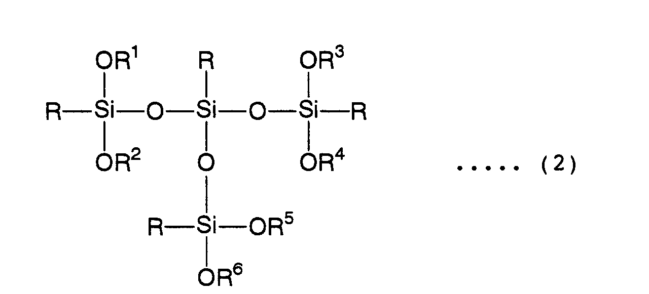
- A photo-curable resin composition according to Claim 1, wherein the organic silicic compound is 3-glycidoxytrimethoxysilane or 3-aminopropyltriethoxysilane, the epoxy resin is bisphenol A epoxy resin, o-cresol novolak epoxy resin or an alicyclic epoxy resin, and the photo initiator is triallylsulfonium hexafluorophosphate.
- A photo-curable resin composition according to Claim 1, wherein said resin composition provides a cured product having a difference in storage modulus of elasticity at TG + 40°C and 25°C of -1.25 to 1.8 GPa and a difference in bonding strength at Tg + 40°C and 25°C of -0.4 to -0.8 kN/m.
- A photo-curable resin composition according to Claim 3, wherein the cured product has at Tg + 40°C a storage modulus of elasticity of 0.4 to 0.55 GPa and a bonding strength of 0.7 to 0.9 kN/m.
- A process for producing a photo-curable resin composition, which comprises a step of heat treating a mixture comprising epoxy resin, an organic silicic compound represented by the following formula (3):where R is an organic group reacting with an epoxy group; and R1 is CH3 or C2H5, and water, and a step of mixing a photo initiator with the heat-treated mixture.

- A process according to Claim 5, wherein the organic silicic compound is 3-glycidoxytrimethoxysilane or 3-aminopropyltriethoxysilane, the epoxy resin is bisphenol A epoxy resin, o-cresol novolak epoxy resin or an alicyclic epoxy resin, and the photo initiator is triallylsulfonium hexafluorophosphate.
- A process for using the photo-curable resin composition of Claim 1 as an insulating layer in a multilayer wiring board.
- A process for using the photo-curable resin composition of Claim 1 as a layer for covering projecting electrodes in a semiconductor device.
- A multilayer wiring board, which comprises conductor layers, insulating layers composed of photo-curable resin composition and formed between the conductor layers and a filler filled in blind via holes interconnecting the conductor layers one to another, wherein at least one of the insulating layers is formed from a photo-curable resin composition, which comprises an organic silicic compound represented by the following general formula (1) or (2):
 where R is an organic group reacting with an epoxy group; and R1 to R6 are independently silicon-containing groups having 0-3 repeat units of (SiRO3/2); in case the unit of (SiRO3/2) is zero, R1 to R6 are independently H, CH3 or C2H6, an epoxy resin and a photo initiator capable of initiating polymerization of the organic silicic compound or the epoxy resin upon absorption of actinic ray.
- A multilayer wiring board according to Claim 9, wherein the organic silicic compound is 3-glycidoxytrimethoxysilane or 3-aminopropyltriethoxysilane, the epoxy resin is bisphenol A epoxy resin, o-cresol novolak epoxy resin or an alicyclic epoxy resin, and the photo initiator is triallylsulfonium hexafluorophosphate.
- A semiconductor device, which comprises a semiconductor component having a projected electrode on the surface, a resin composition covering the projected electrode and a ball electrode connected to the projected electrode exposed from the resin composition, wherein the resin composition is a photo-curable resin composition, which comprises an organic silicic compound represented by the following formula (1) or (2):
 wherein R is an organic group reacting with an epoxy group; and R1 to R6 are independently silicon-containing groups having 0-3 repeat units of (SiRO3/2); in case the unit of (SiRO3/2) is zero, R1 to R6 are independently H, CH3 or CH2CH3, an epoxy resin and a photo initiator capable of initiating polymerization of the organic silicic compound or the epoxy resin upon absorption of actinic ray.
- A semiconductor device according to Claim 11, wherein the organic silicic compound is 3-glycidoxytrimethoxysilane or 3-aminopropyltriethoxysilane, the epoxy resin is bisphenol A epoxy resin, o-cresol novolak epoxy resin or an alicyclic epoxy resin, and the photo initiator is triallylsulfonium hexafluorophosphate.
Applications Claiming Priority (2)
| Application Number | Priority Date | Filing Date | Title |
|---|---|---|---|
| JP2000104031 | 2000-04-05 | ||
| JP2000104031A JP2001288249A (en) | 2000-04-05 | 2000-04-05 | Photocurable resin composition, process for preparation thereof, and product using it |
Publications (2)
| Publication Number | Publication Date |
|---|---|
| EP1142922A2 true EP1142922A2 (en) | 2001-10-10 |
| EP1142922A3 EP1142922A3 (en) | 2002-08-21 |
Family
ID=18617648
Family Applications (1)
| Application Number | Title | Priority Date | Filing Date |
|---|---|---|---|
| EP01104297A Withdrawn EP1142922A3 (en) | 2000-04-05 | 2001-02-22 | Photo-curable resin composition, process for producing the same and products using the same |
Country Status (4)
| Country | Link |
|---|---|
| US (1) | US20010039300A1 (en) |
| EP (1) | EP1142922A3 (en) |
| JP (1) | JP2001288249A (en) |
| KR (1) | KR20010100797A (en) |
Families Citing this family (14)
| Publication number | Priority date | Publication date | Assignee | Title |
|---|---|---|---|---|
| US6818545B2 (en) * | 2001-03-05 | 2004-11-16 | Megic Corporation | Low fabrication cost, fine pitch and high reliability solder bump |
| US6879492B2 (en) * | 2001-03-28 | 2005-04-12 | International Business Machines Corporation | Hyperbga buildup laminate |
| JP2002322343A (en) * | 2001-04-24 | 2002-11-08 | Hitachi Chem Co Ltd | Thermosetting resin composition and method for producing the same |
| US20060235107A1 (en) * | 2005-04-15 | 2006-10-19 | 3M Innovative Properties Company | Method of reusing flexible mold and microstructure precursor composition |
| JP4997105B2 (en) * | 2005-05-23 | 2012-08-08 | イビデン株式会社 | Printed wiring board and manufacturing method thereof |
| WO2008027658A1 (en) * | 2006-09-01 | 2008-03-06 | 3M Innovative Properties Company | Method of making display component with curable paste composition |
| JP2009120770A (en) * | 2007-11-16 | 2009-06-04 | Sekisui Chem Co Ltd | Silicone compound |
| JP2011144386A (en) * | 2011-03-18 | 2011-07-28 | Hitachi Chem Co Ltd | Thermosetting resin composition and method for producing the same |
| JP2012031431A (en) * | 2011-11-04 | 2012-02-16 | Hitachi Chem Co Ltd | Thermosetting resin composition and method of producing the same |
| JP5914123B2 (en) * | 2012-04-11 | 2016-05-11 | 積水化学工業株式会社 | Adhesive for electronic parts and adhesive film for electronic parts |
| JP2021150311A (en) | 2020-03-16 | 2021-09-27 | キオクシア株式会社 | Semiconductor device |
| DE102020123633A1 (en) * | 2020-09-10 | 2022-03-10 | Pac Tech - Packaging Technologies Gmbh | Process for the electroless deposition of a metal layer on a substrate |
| WO2025047498A1 (en) * | 2023-08-31 | 2025-03-06 | 積水化学工業株式会社 | Photocurable resin composition |
| WO2025047496A1 (en) * | 2023-08-31 | 2025-03-06 | 積水化学工業株式会社 | Photocurable resin composition |
Family Cites Families (4)
| Publication number | Priority date | Publication date | Assignee | Title |
|---|---|---|---|---|
| JPS6121126A (en) * | 1984-07-11 | 1986-01-29 | Suriibondo:Kk | Ultraviolet-curable resin composition |
| US5457003A (en) * | 1990-07-06 | 1995-10-10 | Nippon Telegraph And Telephone Corporation | Negative working resist material, method for the production of the same and process of forming resist patterns using the same |
| DE19638630B4 (en) * | 1996-09-20 | 2004-11-18 | Siemens Ag | UV and thermally curable cast resin formulation and their use for the underfilling process in electrical and electronic components |
| JP2000017230A (en) * | 1998-07-02 | 2000-01-18 | Showa Denko Kk | Coating composition containing photocatalyst and method for forming coating film |
-
2000
- 2000-04-05 JP JP2000104031A patent/JP2001288249A/en not_active Withdrawn
-
2001
- 2001-02-22 EP EP01104297A patent/EP1142922A3/en not_active Withdrawn
- 2001-02-23 US US09/790,692 patent/US20010039300A1/en not_active Abandoned
- 2001-02-27 KR KR1020010009871A patent/KR20010100797A/en not_active Withdrawn
Also Published As
| Publication number | Publication date |
|---|---|
| EP1142922A3 (en) | 2002-08-21 |
| JP2001288249A (en) | 2001-10-16 |
| KR20010100797A (en) | 2001-11-14 |
| US20010039300A1 (en) | 2001-11-08 |
Similar Documents
| Publication | Publication Date | Title |
|---|---|---|
| CN101983425B (en) | Multilayer circuit board, insulating sheet, and semiconductor package using multilayer circuit board | |
| EP1142922A2 (en) | Photo-curable resin composition, process for producing the same and products using the same | |
| JP4911795B2 (en) | Manufacturing method of laminate | |
| JP6696113B2 (en) | Resin composition for printed wiring board, prepreg, resin substrate, metal-clad laminate, printed wiring board, and semiconductor device | |
| KR101195408B1 (en) | Semiconductor device | |
| CN1240772C (en) | Phosphorus-containing epoxy resin composition and its application | |
| JP4576794B2 (en) | Insulating resin composition and use thereof | |
| JP4298291B2 (en) | Liquid thermosetting resin composition and printed wiring board | |
| US6190834B1 (en) | Photosensitive resin composition, and multilayer printed circuit board using the same | |
| JP2016196549A (en) | Resin composition for printed wiring board, prepreg, resin substrate, metal clad laminated board, printed wiring board, and semiconductor device | |
| KR101316105B1 (en) | Manufacturing method for printed circuit board containing flame retardant insulating layer | |
| JP2016196557A (en) | Resin composition for printed wiring board, prepreg, resin substrate, metal clad laminated board, printed wiring board, and semiconductor device | |
| KR100893992B1 (en) | Resin paste for die bonding and its use | |
| US6306481B1 (en) | Multilayer circuit board having insulating layer with via-holes | |
| JP5471800B2 (en) | Laminated material for printed wiring board and use thereof | |
| JP2009067852A (en) | Insulation resin sheet impregnated with glass fiber woven fabric, laminated plate, multilayered printed wiring board, and semiconductor device | |
| JPH0864728A (en) | Sealing resin composition, sealing frame composition, semiconductor chip mounting board on which sealing frame is provided and semiconductor device | |
| JP2005175265A (en) | Adhesive sheet for multilayer wiring boards and method for manufacturing multilayer wiring board | |
| JP4385555B2 (en) | Interposer, semiconductor package and manufacturing method thereof | |
| JPH10306202A (en) | Resin composite and adhesive for electroless plating | |
| JP2002134655A (en) | Board for semiconductor package, its manufacturing method, the semiconductor package and its manufacturing method | |
| JP2003234439A (en) | Insulating resin composition | |
| JP2006086233A (en) | Multilayer interconnection board and manufacturing method thereof | |
| JP3522489B2 (en) | Adhesive for electroless plating used for printed wiring boards and printed wiring boards | |
| JP2013065817A (en) | Method for manufacturing printed circuit board |
Legal Events
| Date | Code | Title | Description |
|---|---|---|---|
| PUAI | Public reference made under article 153(3) epc to a published international application that has entered the european phase |
Free format text: ORIGINAL CODE: 0009012 |
|
| AK | Designated contracting states |
Kind code of ref document: A2 Designated state(s): AT BE CH CY DE DK ES FI FR GB GR IE IT LI LU MC NL PT SE TR |
|
| AX | Request for extension of the european patent |
Free format text: AL;LT;LV;MK;RO;SI |
|
| PUAL | Search report despatched |
Free format text: ORIGINAL CODE: 0009013 |
|
| AK | Designated contracting states |
Kind code of ref document: A3 Designated state(s): AT BE CH CY DE DK ES FI FR GB GR IE IT LI LU MC NL PT SE TR |
|
| AX | Request for extension of the european patent |
Free format text: AL;LT;LV;MK;RO;SI |
|
| RIC1 | Information provided on ipc code assigned before grant |
Free format text: 7C 08G 59/40 A, 7G 03F 7/075 B, 7C 08L 63/00 B |
|
| 17P | Request for examination filed |
Effective date: 20020917 |
|
| AKX | Designation fees paid |
Designated state(s): DE FR GB |
|
| 17Q | First examination report despatched |
Effective date: 20030507 |
|
| STAA | Information on the status of an ep patent application or granted ep patent |
Free format text: STATUS: THE APPLICATION IS DEEMED TO BE WITHDRAWN |
|
| 18D | Application deemed to be withdrawn |
Effective date: 20030918 |