EP1139430A1 - Transistor MOS dans un circuit intégré et procédé de formation de zone active - Google Patents
Transistor MOS dans un circuit intégré et procédé de formation de zone active Download PDFInfo
- Publication number
- EP1139430A1 EP1139430A1 EP01410032A EP01410032A EP1139430A1 EP 1139430 A1 EP1139430 A1 EP 1139430A1 EP 01410032 A EP01410032 A EP 01410032A EP 01410032 A EP01410032 A EP 01410032A EP 1139430 A1 EP1139430 A1 EP 1139430A1
- Authority
- EP
- European Patent Office
- Prior art keywords
- spacer
- zone
- active area
- substrate
- insulating
- Prior art date
- Legal status (The legal status is an assumption and is not a legal conclusion. Google has not performed a legal analysis and makes no representation as to the accuracy of the status listed.)
- Granted
Links
Images


Classifications
-
- H—ELECTRICITY
- H10—SEMICONDUCTOR DEVICES; ELECTRIC SOLID-STATE DEVICES NOT OTHERWISE PROVIDED FOR
- H10D—INORGANIC ELECTRIC SEMICONDUCTOR DEVICES
- H10D62/00—Semiconductor bodies, or regions thereof, of devices having potential barriers
- H10D62/10—Shapes, relative sizes or dispositions of the regions of the semiconductor bodies; Shapes of the semiconductor bodies
- H10D62/17—Semiconductor regions connected to electrodes not carrying current to be rectified, amplified or switched, e.g. channel regions
- H10D62/213—Channel regions of field-effect devices
- H10D62/221—Channel regions of field-effect devices of FETs
- H10D62/235—Channel regions of field-effect devices of FETs of IGFETs
- H10D62/299—Channel regions of field-effect devices of FETs of IGFETs having lateral doping variations
-
- H—ELECTRICITY
- H10—SEMICONDUCTOR DEVICES; ELECTRIC SOLID-STATE DEVICES NOT OTHERWISE PROVIDED FOR
- H10D—INORGANIC ELECTRIC SEMICONDUCTOR DEVICES
- H10D84/00—Integrated devices formed in or on semiconductor substrates that comprise only semiconducting layers, e.g. on Si wafers or on GaAs-on-Si wafers
- H10D84/01—Manufacture or treatment
- H10D84/0123—Integrating together multiple components covered by H10D12/00 or H10D30/00, e.g. integrating multiple IGBTs
- H10D84/0126—Integrating together multiple components covered by H10D12/00 or H10D30/00, e.g. integrating multiple IGBTs the components including insulated gates, e.g. IGFETs
- H10D84/0151—Manufacturing their isolation regions
-
- H—ELECTRICITY
- H10—SEMICONDUCTOR DEVICES; ELECTRIC SOLID-STATE DEVICES NOT OTHERWISE PROVIDED FOR
- H10D—INORGANIC ELECTRIC SEMICONDUCTOR DEVICES
- H10D84/00—Integrated devices formed in or on semiconductor substrates that comprise only semiconducting layers, e.g. on Si wafers or on GaAs-on-Si wafers
- H10D84/01—Manufacture or treatment
- H10D84/02—Manufacture or treatment characterised by using material-based technologies
- H10D84/03—Manufacture or treatment characterised by using material-based technologies using Group IV technology, e.g. silicon technology or silicon-carbide [SiC] technology
- H10D84/038—Manufacture or treatment characterised by using material-based technologies using Group IV technology, e.g. silicon technology or silicon-carbide [SiC] technology using silicon technology, e.g. SiGe
-
- H—ELECTRICITY
- H10—SEMICONDUCTOR DEVICES; ELECTRIC SOLID-STATE DEVICES NOT OTHERWISE PROVIDED FOR
- H10W—GENERIC PACKAGES, INTERCONNECTIONS, CONNECTORS OR OTHER CONSTRUCTIONAL DETAILS OF DEVICES COVERED BY CLASS H10
- H10W10/00—Isolation regions in semiconductor bodies between components of integrated devices
- H10W10/01—Manufacture or treatment
- H10W10/011—Manufacture or treatment of isolation regions comprising dielectric materials
- H10W10/014—Manufacture or treatment of isolation regions comprising dielectric materials using trench refilling with dielectric materials, e.g. shallow trench isolations
-
- H—ELECTRICITY
- H10—SEMICONDUCTOR DEVICES; ELECTRIC SOLID-STATE DEVICES NOT OTHERWISE PROVIDED FOR
- H10W—GENERIC PACKAGES, INTERCONNECTIONS, CONNECTORS OR OTHER CONSTRUCTIONAL DETAILS OF DEVICES COVERED BY CLASS H10
- H10W10/00—Isolation regions in semiconductor bodies between components of integrated devices
- H10W10/10—Isolation regions comprising dielectric materials
- H10W10/17—Isolation regions comprising dielectric materials formed using trench refilling with dielectric materials, e.g. shallow trench isolations
Definitions
- the present invention relates, in general, to integrated circuits on semiconductor substrate comprising at least a component formed in an active area and more particularly the formation of active zones surrounded by insulating zones. These insulating zones are obtained from trenches filled with a insulating material and each active area is intended to receive a conductive structure isolated from it, for example a control gate of a transistor type device.
- the device can be a MOS transistor formed by any technology known (MOS, CMOS, BiCMOS).
- FIG. 1 partially and schematically illustrates, in cross section, a semiconductor substrate 1 on which an insulated conductive line is formed.
- this line is an electrode gate of a lateral type MOS transistor.
- the substrate 1 comprises an active zone 5 delimited by an insulating zone 2.
- the insulating zone 2 was formed by digging trenches in the substrate, then by filling them with an insulating material, typically oxide of silicon (SiO 2 ). The filling is carried out so that the insulating material overflows, as indicated by the dotted line 6, relative to the level defined by the substrate, from which it follows that the insulating zone 2 has an apex having a substantially flat surface at a level higher than the surface of the active area 5 thus defined, this vertex ending in a substantially vertical rim leading to the active area 5.
- Such an insulating area structure 2 can be conventionally obtained in various ways, as will be explained below.
- the insulating zone 2 presents, in contact with the zone activates 5, a weakening zone which, following over-etching in subsequent stages of removal of various insulating materials sacrificial, will cause a depression 7 in the periphery active zone 5.
- a thin layer 3 of insulation covers the upper surface of the active area 5 as well as its peripheral part discovered by depression 7.
- Layer 3 is covered with a layer 4 of a conductive material, typically polycrystalline silicon.
- the conductive material 4 passes over the insulating zone 2 and over the active zone 5, and fills the depression 7.
- the filling of the depression 7 by the grid material has annoying effects. Because of the curvature presented on the edge of the active area 5 by the material grid due to this depression, the distribution of electric field in the channel zone at the edge of the zone insulator 2 is disturbed, which deteriorates, as will be seen below, the performance of the transistor.
- Figure 2 illustrates a top view of an MOS transistor lateral type.
- Figure 1 corresponds to a view partial in section along line A-A ', limited by a defined area by the dotted lines.
- Active area 5 includes a channel zone, located under a control grid 4 and, on the other and on the other side of the grid, source and drain regions. The grid, drain and source contact points are highlighted by hatched regions, whose location is indifferent to the disclosure of the present invention.
- the depression 7 presented by the insulating zone 2 is found on the entire periphery P of the active zone 5.
- the portions of the periphery P underlying the grid are set evidence by checkers 8 and we can consider that the transistor MOS of Figure 2 is formed of two transistors: a transistor normal performance central, with its flat grid and parallel to the surface of the substrate 1, and on either side of the central transistor, a parasitic transistor with deteriorated performance located along the insulating zone 2, having a non-planar grid extending over the depression 7.
- FIG. 3 represents the drain-source current Ids, in logarithmic coordinates as a function of gate-source voltage Vgs.
- Curve C2 corresponds to parasitic transistor and has a reduced threshold voltage V2 and an increased leakage current I2off. Like the MOS transistor resulting has a characteristic corresponding to the sum of the two curves C1 and C2, its threshold voltage will also be lowered and above all its leakage current Ioff increased. That provokes leaks, very troublesome for example in applications where the transistor considered is part of a chip powered by a battery, as in mobile phones, the battery being likely to discharge more quickly.
- the harmful effects of parasitic transistor are all the more important as the area active 5 is narrow. Given the constant trend in the semiconductors to the reduction of the dimensions of the transistors, the harmful effect of the parasitic transistor can only be accentuated and, ultimately, the central transistor may no longer exist if the gate width becomes too small, resulting transistor no longer formed except by the parasitic transistor.
- an object of the present invention is to propose a MOS transistor which avoids the drawbacks of the art prior.
- Another object of the present invention is to provide a MOS transistor which has an undamaged voltage threshold.
- Another object of the present invention is to provide a method for forming an active zone in a semiconductor substrate to obtain such a structure.
- the spacer has a substantially vertical rim or has a bell shape, the thickness of which decreases as it moves away from said flange.
- the implantation step is followed by a step of eliminating the spacer.
- the step of eliminating the spacer is preceded or followed by a step of implantation of another active area with a dopant of a other type of conductivity than that of the dopant used in step d).
- the protective coating results from thermal growth a thin layer of silicon oxide on the surface of the substrate.
- the spacer is made of silicon nitride.
- the spacer is made of polycrystalline silicon.
- the present invention also provides a transistor MOS comprising a doped channel zone adjacent to an insulating zone, the dopants present in the part of the channel zone in contact with the insulating area being closer to the surface than the dopants present in the rest of the channel area.
- the present invention also relates to an integrated circuit including such a transistor and a terminal including such a circuit integrated.
- the process according to the invention begins with the definition an active area in the substrate 10, for example made of silicon monocrystalline, by an insulating zone 11 (FIG. 4A).
- Zone 11 is formed by digging trenches in substrate 10 and then filling them with insulating material.
- Zone 11 can be obtained by any known conventional method. This will, for example, be the sequence of the following steps: deposition of a mask, for example made of silicon nitride (Si 3 N 4 ), typically having a thickness of the order of a few tens of nanometers, etching of this mask so as to leave it only at the location of the active area, digging trenches at the location of the insulating area, filling the trenches with insulating material, planarization by aligning with the level of the parts remaining from the mask, then removing the remaining mask.
- a mask for example made of silicon nitride (Si 3 N 4 )
- etching of this mask so as to leave it only at the location of the active area
- digging trenches at the location of the insulating area filling the trenches with insulating material
- planarization by aligning with the level of the parts remaining from the mask,
- the insulating zone is made of so that the insulating material overflows vertically from the trenches, where it follows that its upper surface is at a level higher than that of the active zone.
- Zone 11 has therefore a rim projecting from the surface of the substrate 10 at the periphery of the active area.
- This layer 12 is for example a thermal oxide caused to grow over a thickness typically between 5 and 15 nm, for example 10 nm.
- the layer 13, for example insulating, preferably made of nitride of silicon (Si 3 N 4 ), has a thickness chosen as explained below. It will be noted that, following its deposition, the layer 13 has an extra thickness at the rim presented by the insulating zone 11 at the periphery of the active zone.
- layer 13 is etched so as to eliminate it from the surface upper zone 11.
- this engraving during which the insulating materials of zone 11 and of the layer sacrificial 12 serve as an engraving stop, we leave in place a peripheral spacer 14, due to the excess thickness of the layer 13 at the rim between the upper surface of the zone 11 and the active zone.
- the layer 13 is etched so that the spacer 14 tapers off from the edge of zone 11 on the outskirts of the active area towards the central part of the latter. Then part of the spacer 14 distal of the edge of the zone 11, instead to have a substantially vertical wall, has a shape in "bell".
- Those skilled in the art will know how to implement methods suitable for modulating the reduction in thickness of the lower part of the spacer 14.
- Those skilled in the art will also know choose the etching conditions and the thickness of the thick insulating layer 13 so as to obtain a spacer 14 of desired width.
- the spacer 14 formed can also have a substantially vertical wall, as illustrated in Figure 4B '.
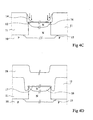
- the substrate is P-type and the area active shown has a type N box. of the active zone takes place while the spacer 14 is in place at the periphery of the active area, as illustrated by downward vertical arrows, where it follows that the dopants implanted are slowed down and penetrate less deeply into the substrate 10 at the periphery, in the area covered by the spacer.
- At least two successive implantations of similar dopants a first high energy implantation intended to form a box 15 deep N type and lightly doped, reaching the substrate 10 below zone 11, and at least one location at a lower level energy intended to more specifically adjust the doping of the zone active.
- Profile 16 resulting from this second implantation is modified at the periphery due to the presence of the spacer 14. This zone 16 corresponds to the effective channel zone.
- the spacer 14 can be kept in place during the formation, in another active area, of different type, for example P. According to another embodiment, the spacer 14 is only held in place during the production of type N boxes in the type P substrate.
- an insulation of grid 17 is deposited and etched a conductive material, for example polycrystalline silicon, so as to form the grid of the structure. Layer 18 fills the depression in zone 11.
- the threshold voltage of the parasitic transistor is raised and this compensates for the drop caused by the fact that the material of grid fills the peripheral depression of the active area.
- the resulting MOS transistor does not show any lowering of its threshold voltage and its leakage current Ioff does not increase not.
- the characteristics of the MOS transistor formed are not degraded and correspond substantially to those of the central transistor.
- the dimensions of the active area can advantageously be reduced.
- Another advantage of the present invention is to allow, after doping of the active area, a "planing" of the top of the insulating zone, which can even have a surface slightly below the surface of the substrate.
- accentuation of the depression of the insulating zone 11 peripheral to the active area caused by such planing does not alter the characteristics of the overall transistor made of the modified doping profile. This allows better planarization, useful in the later stages of manufacturing of the integrated circuit.
- layer 13 is made of an insulating material, preferably silicon nitride.
- insulating material preferably silicon nitride.
- insulating or not we can choose another material, insulating or not, provided that the conditions of selective etching exposed are respected previously. It may for example be polycrystalline silicon or amorphous.
Landscapes
- Insulated Gate Type Field-Effect Transistor (AREA)
- Element Separation (AREA)
- Metal-Oxide And Bipolar Metal-Oxide Semiconductor Integrated Circuits (AREA)
Abstract
Description
Claims (11)
- Procédé de formation d'une zone active entourée d'une zone isolante (11) dans un substrat semiconducteur (10), comprenant les étapes suivantes :a) former, dans le substrat, une tranchée entourant une zone active ;b) remplir la tranchée d'un matériau isolant (11) de façon à former un rebord dépassant de la surface du substrat à la périphérie de la zone active ;c) former un espaceur (14) à la périphérie dudit rebord ; etd) effectuer une implantation d'un dopant, d'où il résulte que l'implantation dans la zone située sous l'espaceur est moins profonde que dans le reste de la zone active.
- Procédé selon la revendication 1, dans lequel l'espaceur (14) présente un rebord sensiblement vertical ou a une forme en cloche, dont l'épaisseur s'amenuise en s'éloignant dudit rebord.
- Procédé selon la revendication 1, dans lequel l'étape d'implantation est suivie d'une étape d'élimination de l'espaceur (14).
- Procédé selon la revendication 3, dans lequel l'étape d'élimination de l'espaceur (14) est précédée ou suivie d'une étape d'implantation d'une autre zone active avec un dopant d'un autre type de conductivité que celle du dopant utilisé à l'étape d).
- Procédé selon la revendication 1, dans lequel, entre l'étape de remplissage de la tranchée et l'étape c) de formation d'un espaceur, est prévue une étape consistant à former, à la surface de la zone active, un revêtement de protection (12).
- Procédé selon la revendication 5, dans lequel le revêtement de protection (12) résulte de la croissance thermique d'une couche mince d'oxyde de silicium à la surface du substrat (10).
- Procédé selon l'une quelconque des revendications 1 à 6, dans lequel l'espaceur est en nitrure de silicium.
- Procédé selon l'une quelconque des revendications 1 à 6, dans lequel l'espaceur (14) est en silicium polycristallin.
- Transistor MOS comportant une zone de canal effective dopée adjacente à une tranchée remplie d'un isolant (11), caractérisé en ce que les dopants présents dans la partie de la zone de canal en contact avec la zone isolante sont plus proches de la surface que les dopants présents dans le reste de la zone de canal.
- Circuit intégré sur un substrat semiconducteur comprenant au moins un transistor selon la revendication 9.
- Terminal mobile comprenant un circuit intégré selon la revendication 10.
Applications Claiming Priority (2)
| Application Number | Priority Date | Filing Date | Title |
|---|---|---|---|
| FR0004174 | 2000-03-31 | ||
| FR0004174A FR2807206A1 (fr) | 2000-03-31 | 2000-03-31 | Transistor mos dans un circuit integre et procede de formation de zone active |
Publications (2)
| Publication Number | Publication Date |
|---|---|
| EP1139430A1 true EP1139430A1 (fr) | 2001-10-04 |
| EP1139430B1 EP1139430B1 (fr) | 2008-10-08 |
Family
ID=8848759
Family Applications (1)
| Application Number | Title | Priority Date | Filing Date |
|---|---|---|---|
| EP01410032A Expired - Lifetime EP1139430B1 (fr) | 2000-03-31 | 2001-03-29 | Transistor MOS dans un circuit intégré et procédé de formation de zone active |
Country Status (5)
| Country | Link |
|---|---|
| US (1) | US6746935B2 (fr) |
| EP (1) | EP1139430B1 (fr) |
| JP (1) | JP2001319889A (fr) |
| DE (1) | DE60136026D1 (fr) |
| FR (1) | FR2807206A1 (fr) |
Families Citing this family (2)
| Publication number | Priority date | Publication date | Assignee | Title |
|---|---|---|---|---|
| US6864148B1 (en) | 2003-09-05 | 2005-03-08 | Mosel Vitelic, Inc. | Corner protection to reduce wrap around |
| KR100741876B1 (ko) * | 2005-07-21 | 2007-07-23 | 동부일렉트로닉스 주식회사 | 디보트가 방지된 트렌치 소자분리막이 형성된 반도체 소자의 제조 방법 |
Citations (6)
| Publication number | Priority date | Publication date | Assignee | Title |
|---|---|---|---|---|
| GB1075085A (en) * | 1964-07-13 | 1967-07-12 | Associated Semiconductor Mft | Improvements in or relating to semiconductor devices |
| DE2641334A1 (de) * | 1976-09-14 | 1978-03-16 | Siemens Ag | Verfahren zur herstellung integrierter mis-schaltungen |
| GB2030769A (en) * | 1978-09-29 | 1980-04-10 | Siemens Ag | Field effect transistor |
| US5132755A (en) * | 1989-07-11 | 1992-07-21 | Oki Electric Industry Co. Ltd. | Field effect transistor |
| US5357137A (en) * | 1991-08-28 | 1994-10-18 | Nec Corporation | Semiconductor device |
| US5424571A (en) * | 1992-03-30 | 1995-06-13 | Sgs-Thomson Microelectronics, Inc. | Sloped spacer for mos field effect devices |
Family Cites Families (13)
| Publication number | Priority date | Publication date | Assignee | Title |
|---|---|---|---|---|
| JPH04297055A (ja) * | 1991-03-26 | 1992-10-21 | Sharp Corp | 半導体装置の製造方法 |
| JPH0529310A (ja) * | 1991-07-24 | 1993-02-05 | Nec Corp | 半導体装置の製造方法 |
| JPH07273330A (ja) * | 1994-03-31 | 1995-10-20 | Toshiba Corp | 半導体装置及びその製造方法 |
| US5539229A (en) * | 1994-12-28 | 1996-07-23 | International Business Machines Corporation | MOSFET with raised STI isolation self-aligned to the gate stack |
| US6281562B1 (en) * | 1995-07-27 | 2001-08-28 | Matsushita Electric Industrial Co., Ltd. | Semiconductor device which reduces the minimum distance requirements between active areas |
| US5777370A (en) * | 1996-06-12 | 1998-07-07 | Advanced Micro Devices, Inc. | Trench isolation of field effect transistors |
| US5994202A (en) * | 1997-01-23 | 1999-11-30 | International Business Machines Corporation | Threshold voltage tailoring of the corner of a MOSFET device |
| US6097076A (en) * | 1997-03-25 | 2000-08-01 | Micron Technology, Inc. | Self-aligned isolation trench |
| JPH11274486A (ja) * | 1998-03-25 | 1999-10-08 | Toshiba Corp | 半導体装置およびその製造方法 |
| US6077748A (en) * | 1998-10-19 | 2000-06-20 | Advanced Micro Devices, Inc. | Advanced trench isolation fabrication scheme for precision polysilicon gate control |
| US5950090A (en) * | 1998-11-16 | 1999-09-07 | United Microelectronics Corp. | Method for fabricating a metal-oxide semiconductor transistor |
| TW413921B (en) * | 1999-03-02 | 2000-12-01 | United Microelectronics Corp | Manufacturing method of multi-threshold voltage device |
| US6261924B1 (en) * | 2000-01-21 | 2001-07-17 | Infineon Technologies Ag | Maskless process for self-aligned contacts |
-
2000
- 2000-03-31 FR FR0004174A patent/FR2807206A1/fr not_active Withdrawn
-
2001
- 2001-03-29 EP EP01410032A patent/EP1139430B1/fr not_active Expired - Lifetime
- 2001-03-29 US US09/823,274 patent/US6746935B2/en not_active Expired - Lifetime
- 2001-03-29 DE DE60136026T patent/DE60136026D1/de not_active Expired - Lifetime
- 2001-03-30 JP JP2001097867A patent/JP2001319889A/ja active Pending
Patent Citations (6)
| Publication number | Priority date | Publication date | Assignee | Title |
|---|---|---|---|---|
| GB1075085A (en) * | 1964-07-13 | 1967-07-12 | Associated Semiconductor Mft | Improvements in or relating to semiconductor devices |
| DE2641334A1 (de) * | 1976-09-14 | 1978-03-16 | Siemens Ag | Verfahren zur herstellung integrierter mis-schaltungen |
| GB2030769A (en) * | 1978-09-29 | 1980-04-10 | Siemens Ag | Field effect transistor |
| US5132755A (en) * | 1989-07-11 | 1992-07-21 | Oki Electric Industry Co. Ltd. | Field effect transistor |
| US5357137A (en) * | 1991-08-28 | 1994-10-18 | Nec Corporation | Semiconductor device |
| US5424571A (en) * | 1992-03-30 | 1995-06-13 | Sgs-Thomson Microelectronics, Inc. | Sloped spacer for mos field effect devices |
Non-Patent Citations (1)
| Title |
|---|
| TANG X ET AL: "INTRINSIC MOSFET PARAMETER FLUCTUATIONS DUE TO RANDOM DOPANT PLACEMENT", IEEE TRANSACTIONS ON VERY LARGE SCALE INTEGRATION (VLSI) SYSTEMS,US,IEEE INC. NEW YORK, vol. 5, no. 4, 1 December 1997 (1997-12-01), pages 369 - 376, XP000723679, ISSN: 1063-8210 * |
Also Published As
| Publication number | Publication date |
|---|---|
| EP1139430B1 (fr) | 2008-10-08 |
| US6746935B2 (en) | 2004-06-08 |
| US20020076868A1 (en) | 2002-06-20 |
| FR2807206A1 (fr) | 2001-10-05 |
| DE60136026D1 (de) | 2008-11-20 |
| JP2001319889A (ja) | 2001-11-16 |
Similar Documents
| Publication | Publication Date | Title |
|---|---|---|
| EP1145300B1 (fr) | Procede de fabrication d'un transistor mis sur un substrat semi-conducteur | |
| FR2812970A1 (fr) | Transistor a effet de champ de type metal-oxyde-semiconducteur a sillicium sur isolant et son procede de fabrication | |
| FR2823009A1 (fr) | Procede de fabrication d'un transistor vertical a grille isolee a faible recouvrement de la grille sur la source et sur le drain, et circuit integre comportant un tel transistor | |
| FR2821483A1 (fr) | Procede de fabrication d'un transistor a grille isolee et a architecture du type substrat sur isolant, et transistor correspondant | |
| EP2779223B1 (fr) | Procédé de réalisation d'un substrat muni d'une protection de bord | |
| FR2990295A1 (fr) | Procede de formation de contacts de grille, de source et de drain sur un transistor mos | |
| EP2610915A1 (fr) | Transistor et procédé de fabrication d'un transistor | |
| FR2860919A1 (fr) | Structures et procedes de fabrication de regions semiconductrices sur isolant | |
| EP1292991B1 (fr) | Procédé de fabrication d'un transistor MOS vertical à grille enterrée | |
| FR3080486A1 (fr) | Procede de formation d'un dispositif microelectronique | |
| EP0996146A1 (fr) | Procédé de formation d'un caisson isolé dans une plaquette de silicium | |
| FR3067516A1 (fr) | Realisation de regions semiconductrices dans une puce electronique | |
| FR3068507A1 (fr) | Realisation de regions semiconductrices dans une puce electronique | |
| FR2953062A1 (fr) | Diode de protection bidirectionnelle basse tension | |
| EP1139430B1 (fr) | Transistor MOS dans un circuit intégré et procédé de formation de zone active | |
| EP0675544A1 (fr) | Procédé de fabrication d'un transistor à effet de champ à grille isolée de longueur de canal réduite, et transistor correspondant | |
| FR2858877A1 (fr) | Transistor bipolaire a heterojonction | |
| FR3078197A1 (fr) | Dispositif de transistor bipolaire et procede de fabrication correspondant | |
| EP1096557A1 (fr) | Procédé de définition de deux zones autoalignées à la surface supérieure d'un substrat | |
| FR2976401A1 (fr) | Composant electronique comportant un ensemble de transistors mosfet et procede de fabrication | |
| FR2952225A1 (fr) | Procede de formation d'un transistor mos a canal en silicium-germanium | |
| EP0607075B1 (fr) | Composant électronique semi-conducteur à résistance dynamique négative, méthodes d'utilisation et procédé de fabrication correspondants | |
| FR3069702A1 (fr) | Procede de fabrication simultanee de transistors soi et de transistors sur substrat massif | |
| FR3138965A1 (fr) | Transistor MOSFET | |
| EP1968106B1 (fr) | Procédé de fabrication d'un transistor à effet de champ à grilles auto-alignées |
Legal Events
| Date | Code | Title | Description |
|---|---|---|---|
| PUAI | Public reference made under article 153(3) epc to a published international application that has entered the european phase |
Free format text: ORIGINAL CODE: 0009012 |
|
| AK | Designated contracting states |
Kind code of ref document: A1 Designated state(s): DE FR GB IT Kind code of ref document: A1 Designated state(s): AT BE CH CY DE DK ES FI FR GB GR IE IT LI LU MC NL PT SE TR |
|
| AX | Request for extension of the european patent |
Free format text: AL;LT;LV;MK;RO;SI |
|
| RAP1 | Party data changed (applicant data changed or rights of an application transferred) |
Owner name: KONINKLIJKE PHILIPS ELECTRONICS N.V. Owner name: STMICROELECTRONICS S.A. |
|
| 17P | Request for examination filed |
Effective date: 20020321 |
|
| AKX | Designation fees paid |
Free format text: DE FR GB IT |
|
| RAP1 | Party data changed (applicant data changed or rights of an application transferred) |
Owner name: STMICROELECTRONICS S.A. Owner name: NXP B.V. |
|
| RIC1 | Information provided on ipc code assigned before grant |
Ipc: H01L 21/8234 20060101ALI20080229BHEP Ipc: H01L 29/10 20060101AFI20080229BHEP Ipc: H01L 21/762 20060101ALI20080229BHEP Ipc: H01L 21/336 20060101ALI20080229BHEP |
|
| GRAP | Despatch of communication of intention to grant a patent |
Free format text: ORIGINAL CODE: EPIDOSNIGR1 |
|
| GRAS | Grant fee paid |
Free format text: ORIGINAL CODE: EPIDOSNIGR3 |
|
| GRAA | (expected) grant |
Free format text: ORIGINAL CODE: 0009210 |
|
| AK | Designated contracting states |
Kind code of ref document: B1 Designated state(s): DE FR GB IT |
|
| REG | Reference to a national code |
Ref country code: GB Ref legal event code: FG4D Free format text: NOT ENGLISH |
|
| REF | Corresponds to: |
Ref document number: 60136026 Country of ref document: DE Date of ref document: 20081120 Kind code of ref document: P |
|
| PLBE | No opposition filed within time limit |
Free format text: ORIGINAL CODE: 0009261 |
|
| STAA | Information on the status of an ep patent application or granted ep patent |
Free format text: STATUS: NO OPPOSITION FILED WITHIN TIME LIMIT |
|
| PG25 | Lapsed in a contracting state [announced via postgrant information from national office to epo] |
Ref country code: IT Free format text: LAPSE BECAUSE OF FAILURE TO SUBMIT A TRANSLATION OF THE DESCRIPTION OR TO PAY THE FEE WITHIN THE PRESCRIBED TIME-LIMIT Effective date: 20081008 |
|
| 26N | No opposition filed |
Effective date: 20090709 |
|
| REG | Reference to a national code |
Ref country code: DE Ref legal event code: R084 Ref document number: 60136026 Country of ref document: DE |
|
| REG | Reference to a national code |
Ref country code: DE Ref legal event code: R084 Ref document number: 60136026 Country of ref document: DE Effective date: 20141015 |
|
| REG | Reference to a national code |
Ref country code: FR Ref legal event code: PLFP Year of fee payment: 15 |
|
| REG | Reference to a national code |
Ref country code: FR Ref legal event code: PLFP Year of fee payment: 16 |
|
| REG | Reference to a national code |
Ref country code: FR Ref legal event code: PLFP Year of fee payment: 17 |
|
| REG | Reference to a national code |
Ref country code: FR Ref legal event code: PLFP Year of fee payment: 18 |
|
| PGFP | Annual fee paid to national office [announced via postgrant information from national office to epo] |
Ref country code: DE Payment date: 20200218 Year of fee payment: 20 Ref country code: GB Payment date: 20200221 Year of fee payment: 20 |
|
| PGFP | Annual fee paid to national office [announced via postgrant information from national office to epo] |
Ref country code: FR Payment date: 20200220 Year of fee payment: 20 |
|
| REG | Reference to a national code |
Ref country code: DE Ref legal event code: R071 Ref document number: 60136026 Country of ref document: DE |
|
| REG | Reference to a national code |
Ref country code: GB Ref legal event code: PE20 Expiry date: 20210328 |
|
| PG25 | Lapsed in a contracting state [announced via postgrant information from national office to epo] |
Ref country code: GB Free format text: LAPSE BECAUSE OF EXPIRATION OF PROTECTION Effective date: 20210328 |