EP1135236B1 - Reverse linear polisher with loadable housing - Google Patents
Reverse linear polisher with loadable housing Download PDFInfo
- Publication number
- EP1135236B1 EP1135236B1 EP99959045A EP99959045A EP1135236B1 EP 1135236 B1 EP1135236 B1 EP 1135236B1 EP 99959045 A EP99959045 A EP 99959045A EP 99959045 A EP99959045 A EP 99959045A EP 1135236 B1 EP1135236 B1 EP 1135236B1
- Authority
- EP
- European Patent Office
- Prior art keywords
- wafer
- pad
- polishing
- housing
- pin housing
- Prior art date
- Legal status (The legal status is an assumption and is not a legal conclusion. Google has not performed a legal analysis and makes no representation as to the accuracy of the status listed.)
- Expired - Lifetime
Links
Images


Classifications
-
- H10P52/00—
-
- B—PERFORMING OPERATIONS; TRANSPORTING
- B24—GRINDING; POLISHING
- B24B—MACHINES, DEVICES, OR PROCESSES FOR GRINDING OR POLISHING; DRESSING OR CONDITIONING OF ABRADING SURFACES; FEEDING OF GRINDING, POLISHING, OR LAPPING AGENTS
- B24B21/00—Machines or devices using grinding or polishing belts; Accessories therefor
- B24B21/04—Machines or devices using grinding or polishing belts; Accessories therefor for grinding plane surfaces
-
- B—PERFORMING OPERATIONS; TRANSPORTING
- B24—GRINDING; POLISHING
- B24B—MACHINES, DEVICES, OR PROCESSES FOR GRINDING OR POLISHING; DRESSING OR CONDITIONING OF ABRADING SURFACES; FEEDING OF GRINDING, POLISHING, OR LAPPING AGENTS
- B24B37/00—Lapping machines or devices; Accessories
- B24B37/04—Lapping machines or devices; Accessories designed for working plane surfaces
-
- B—PERFORMING OPERATIONS; TRANSPORTING
- B24—GRINDING; POLISHING
- B24B—MACHINES, DEVICES, OR PROCESSES FOR GRINDING OR POLISHING; DRESSING OR CONDITIONING OF ABRADING SURFACES; FEEDING OF GRINDING, POLISHING, OR LAPPING AGENTS
- B24B47/00—Drives or gearings; Equipment therefor
- B24B47/02—Drives or gearings; Equipment therefor for performing a reciprocating movement of carriages or work- tables
- B24B47/04—Drives or gearings; Equipment therefor for performing a reciprocating movement of carriages or work- tables by mechanical gearing only
Definitions
- the present invention relates to the field of chemical mechanical polishing. More particularly, the present invention relates to a method and apparatus for polishing a semiconductor wafer to a high degree of planarity and uniformity. This is achieved when the semiconductor wafer is polished with pads at high bi-directional linear or reciprocating speeds.
- CMP Chemical mechanical polishing
- CMP is a semiconductor wafer flattening and polishing process that combines chemical removal of semiconductor layers such as insulators, metals, and photoresists with mechanical buffering of a wafer surface.
- CMP is generally used to flatten/polish wafers after crystal growing during the wafer fabrication process, and is a process that provides global planarization of the wafer surface.
- CMP is often used to flatten/polish the profiles that build up in multilevel metal interconnection schemes. Achieving the desired flatness of the wafer surface must take place without contaminating the desired surface. Also, the CMP process must avoid polishing away portions of the functioning circuit parts.
- One conventional CMP process requires positioning a wafer on a holder rotating about a first axis and lowered onto a polishing pad rotating in the opposite direction about a second axis.
- the wafer holder presses the wafer against the polishing pad during the planarization process.
- a polishing agent or slurry is typically applied to the polishing pad to polish the wafer.
- a wafer holder positions and presses a wafer against a belt-shaped polishing pad while the pad is moved continuously in the same linear direction relative to the wafer.
- the so-called belt-shaped polishing pad is movable in one continuous path during this polishing process.
- These conventional polishing processes may further include a conditioning station positioned in the path of the polishing pad for conditioning the pad during polishing.
- Factors that need to be controlled to achieve the desired flatness and planarity include polishing time, pressure between the wafer and pad, speed of rotation, slurry particle size, slurry feed rate, the chemistry of the slurry, and pad material.
- CMP is a labor intensive and expensive process because the thickness and uniformity of the layers on the substrate surface must be constantly monitored to prevent over-polishing or inconsistent polishing of the wafer surface.
- EP-A-0517594 discloses a polishing machine having an abrasive belt tensioned between a feeding spool and a receiving spool. A head is provided for supporting a specimen such that a face of the specimen is polished by the abrasive belt.
- a chemical mechanical polishing device for polishing a surface of a semiconductor wafer, the polishing device comprising: a wafer housing adapted to support the wafer; and a polishing station having a pad that polishes the surface of the wafer with bi-directional linear movement.
- a method of polishing a surface of a semiconductor wafer comprising the steps of: supporting the wafer such that the surface of the wafer is exposed to a polishing pad; and, characterised by polishing the surface of the wafer by moving the polishing pad bi-directional linearly.
- a method and apparatus are provided that polish a wafer with a pad having high bi-directional linear speeds.
- preferred embodiments of the present invention include a polishing pad secured to a timing belt mechanism that allows the pad to move in a reciprocating manner, i.e. in both forward and reverse directions, at high speeds.
- the constant forward and reverse movement of the polishing pad as it polishes the wafer provides superior planarity and uniformity across the wafer surface.
- the wafer housing of an embodiment of the present invention can also be used to securely hold the wafer as it is being polished.
- This invention is directed to a CMP method and apparatus that can operate at high bi-directional linear pad or reciprocating speeds and a reduced foot-print.
- the high bi-directional linear pad speeds optimize planarity efficiency while the reduced foot-print reduces the cost of the polishing station.
- the polishing pad is adapted to travel in bi-directional linear directions, this reduces the pad glazing effect, which is a common problem in conventional CMP polishers. Because the pad travels in bi-directional linear directions, the pad is substantially self conditioning.
- Fig. 1 illustrates a perspective view
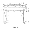
- Fig. 2 illustrates a side view of an apparatus of a preferred embodiment of the invention.
- the wafer polishing station 2 includes a bi-directional linear, or reverse linear, polisher 3 and a wafer housing 4.
- the wafer housing 4 (which can rotate about its center axis and move side to side, as known) securely positions a wafer 18 so that a surface 17 may be polished.
- a novel method and apparatus of loading and unloading the wafer 18 onto the wafer housing 4 is described more fully later herein.
- the reverse linear polisher 3 includes a polishing pad 6 for polishing the wafer surface 17, a mechanism 8 for driving the polishing pad 6 in a bi-directional linear or reciprocating (forward and reverse) motion, and a support plate 10 for supporting the pad 6 as the pad 6 polishes the wafer surface 17.
- a polishing agent or slurry containing a chemical that oxidizes and mechanically removes a wafer layer is flowed between the wafer 18 and the polishing pad 6.
- the polishing agent or slurry such as colloidal silica or fumed silica is generally used.
- the polishing agent or slurry generally grows a thin layer of silicon dioxide or oxide on the wafer surface 17, and the buffering action of the polishing pad 6 mechanically removes the oxide.
- the size of the particles from the polishing agent or slurry used to polish the wafer surface 17 is preferably at least two or three times larger than the feature size of the wafer surface 17. For example, if the feature size of the wafer surface 17 is 1 micron, then the size of the particles should be at least 2 or 3 microns.
- the underside of the polishing pad 6 is attached to a flexible but firm and flat material (not shown) for supporting the pad 6.
- the polishing pad 6 is generally a stiff polyurethane material, although other suitable materials may be used that is capable of polishing wafer surface 17.
- Driving mechanism 8 includes three timing belts, two vertically suspending timing belts 14, 15 and one horizontally suspending timing belt 16.
- the timing belts 14, 15, and 16 may be formed of any suitable material such as stainless steel or high strength polymers having sufficient strength to withstand the load applied to the belts by the wafer 18.
- One end of the vertically suspending timing belts 14, 15 is secured to rollers 20 while the other end is secured to rollers 22.
- each end of the horizontally suspending timing belt 16 is secured to rollers 20. As illustrated in Fig. 1, it is noted that the horizontally suspending timing belt 16 is placed in a z-plane slightly outside the z-plane of the vertically suspending timing belts 14, 15.
- Rollers 20 link the two vertically suspending timing belts 14, 15 with the horizontally suspending timing belt 16 so that each belts rate of rotation depends on the rate of rotation of the other belts.
- the rollers 20 and 22 retain the timing belts 14, 15, and 16 under proper tension so that the polishing pad 6 is sufficiently rigid to uniformly polish the wafer surface 17.
- the tension of the timing belts may be increased or decreased as needed by adjusting the position of rollers 22 relative to roller 20.
- the invention describes a driving mechanism having three timing belts secured on four rollers, it is understood that any suitable number of rollers and/or timing belts, or a driving mechanism that does not rely on rollers/belts, i.e. a seesaw mechanism, such that it provides the bi-directional linear or reciprocating motion, are intended to be within the scope and spirit of the invention.
- the polishing pad 6 and the corresponding support material is adapted to bend at an angle at corners 24, which angle is preferably about 90°.
- Each end of the polishing pad 6 is attached to a point on the two vertically positioned timing belts 14, 15 by attachment 12, 13.
- One end of the polishing pad 6 is secured to attachment 12, and the other end is secured to attachment 13.
- Attachments 12 and 13 are preferably a sleeve and rod, as more fully described later herein. Referring again to Figs. 1 and 2, as one end of the polishing pad 6 travels vertically downward with the assistance of timing belt 14 and attachment 12, the other end of the polishing pad 6 travels vertically upward with the assistance of timing belt 15 and attachment 13.
- the mechanical alignment of the timing belts 14, 15, and 16 with the rollers 20 and 22 allows such movement to occur.
- a conventional motor (not shown) is used to rotate rollers 20 and/or 22.
- the motor is connected to rollers 20 or 22 or to any suitable element connected to rollers 20 and/or 22, and it provides the necessary torque to rotate rollers 20 and 22 to a desired rate of rotation.
- the motor directly/indirectly causes rollers 20 and 22 to rotate so that the timing belts 14, 15, and 16 are driven at a desired speed in both forward and reverse directions. For instance, when attachment 13 reaches roller 22 during its downward motion, it will reverse the direction of the polishing pad 6 as attachment 13 now travels upward. Soon thereafter, the same attachment 13 now reaches roller 20 and again changes direction in a downward direction.
- the reciprocating movement of attachment 13 allows the polishing pad 6 to move in both forward and reverse directions.
- the speed at which the polishing pad 6 is moved is within the range of approximately 100 to 600 feet per minute for optimum planarization of the wafer surface 17.
- the speed of the polishing pad 6 may vary expending on many factors (size of wafer, type of pad, chemical composition of slurry, etc.).
- the pad 6 may be moved in both bi-directional linear directions at a predetermined speed, which preferably averages between 100 to 600 feet per minute (approximately 1 / 2 to 3 ms -1 ).
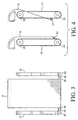
- Fig. 3 illustrates a front view
- Fig. 4 illustrates a side view of a method and apparatus for attaching the polishing pad 6 to the timing belts 14, 15 in accordance with the preferred embodiment of the present invention.
- the underside of the polishing pad 6 is attached to the flexible but firm and flat material, which is non-stretchable.
- a rod 40 is attached at each end of the material, and thus the ends of the polishing pad 6, a rod 40 is attached.
- the rod 40 extends horizontally from the pad 6 as shown in Fig. 3.
- a sleeve 42 i.e.
- a cylinder or a slit is also attached to each of the vertically suspending timing belts 14, 15, and a portion 44 of the sleeve 42 extends horizontally to join the rod 40, as again illustrated in Fig. 3.
- Fig. 4 further illustrates a side view of the polishing pad 6 as it rotates around the rollers 20, 22.
- the polishing pad 6 bends at an angle, preferably about 90° at the two comers 24. This approach is beneficial for various reasons.
- the length of the polishing pad 6 on the horizontal plane needed to polish the wafer surface 17 needs to be only slightly longer than the wafer 18 diameter.
- the entire length of polishing pad should be only slightly longer than three times the wafer 18 diameter. This allows the most efficient and economical use of the entire polishing pad 6.
- slurry or other agent may be applied to the portions of the polishing pad 6 that are not in contact with the wafer surface 17.
- the slurry or other agent can be applied to the polishing pad preferably at locations near comers 24.
- the configuration of the polishing pad 6 described above also decreases the size of a support plate 10 needed to support the pad 6.
- a conditioning member can also be disposed on or about this same location.
- the CMP device of the present invention takes up less space than most traditional CMP devices because about two-thirds of the polishing pad 6 can be in a vertical position.
- the bi-directional linear movement of the CMP device further increases the pad usage efficiency because the reciprocating movement of the pad 6 provides a self-conditioning function, since the pad 6 is moving in different, preferably opposite, directions.
- the polishing pad 6 moves bi-directional with high linear speeds so as to uniformly polish the wafer surface 17. Because high pad speeds are needed to the polish wafer surface 17, the momentum, and thus inertia created is very high. Thus, as the polishing pad 6 reverses direction, sufficient energy is needed to keep the pad moving at desired speeds. If the total area (length and width) of the polishing pad 6 is minimized, the energy needed to keep the pad moving at desired speeds is decreased accordingly. Thus, by limiting the length of the polishing pad 6, a conventional motor can handle the necessary energy needed to keep the pad moving at desired speeds in both forward and reverse directions.
- the entire length of the polishing pad 6 should be slightly longer than two-diameter lengths of the wafer 18, and preferably three-diameter lengths of the wafer 18. The reason for this is so that the polishing pad 6 may be conditioned and slurry may be applied to both sides of the pad opposite where the wafer 18 is positioned, in close proximity to corners 24.
- Slurry (not shown) can be applied to the surface of the polishing pad 6 in conventional manners and the pad 6 can also further be conditioned in conventional manners.
- Wafer housing 4 includes a nonconductive, preferably circular, head assembly 28 with a cavity 29 that is preferably a few millimeters deep at its center and having a resting pad 30 thereof.
- the wafer 18 is loaded into the cavity 29, backside first, against the resting pad 30.
- a conventional type of securing mechanism 31 i.e. vacuum
- the resting pad 30 may also be of a type that secures the wafer 18 by suctioning the backside of wafer 18 when the resting pad 30 is wet.
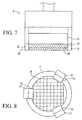
- the reverse linear polisher 3 may polish the wafer 18 during various stages of the wafer fabrication process. Accordingly, a method for loading the wafer 18 into the cavity 29 so that an additional loading mechanism is not needed will now be described with reference to Fig. 6.
- the wafer housing 4 is aligned to load the wafer 18 into the cavity 29.
- the head assembly 28 includes a pin housing 32 adapted to move up and down with respect to the cavity 29 using a motor or pneumatic control (not shown). During loading of the wafer 18, the pin housing 32 extends down from an original position, which is illustrated by the dashed lines, below the surface 17 of the wafer 18.
- At least three pins 34 are then automatically caused to protrude out of the pin housing 32 using a conventional retraction device under motor control so that the wafer 18 can be picked up and loaded into the cavity 29 of the head assembly 28. With the pins 34 protruding out, the pin housing 32 automatically retracts back to its original position, and thus the wafer 18 is loaded into cavity 29. When the head assembly 28 and the resting pad 30 secures the position of the wafer 18, as described above, the pins 34 automatically retract back into the pin housing 32 and the pin housing 32 retracts back to its original position so that the wafer 18 may be polished, as illustrated in Fig. 7.
- the wafer housing 4 is automatically lowered until the wafer surface 17 is in contact with the polishing pad 6.
- the polishing pad 6 polishes the wafer surface 17 in accordance with the method described herein; the wafer 18 is then ready to be unloaded from the wafer housing 4.
- the wafer 18 is unloaded from the wafer housing 4 using essentially a reverse order of the loading steps.
- the wafer housing 4 is raised from the polishing pad 6, and the pin housing 32 extends down from its original position, which is illustrated by the dashed lines, below the surface 17 of the wafer 18.
- the pins 34 are then automatically caused to protrude out so that the wafer 18 may be supported when unloaded from the cavity 29.
- the vacuum is reversed with opposite air flow, thus dropping the wafer 18 away from head assembly 28 and onto the pins 34, i.e., wafer 18 is positioned from the resting pad 30 onto the pins 34. From this position, the wafer can then be transported to the next fabrication processing station.
- Fig. 8 illustrates a bottom view of the wafer 18 surface being loaded and unloaded into the cavity 29 by the pins 34. Although Fig. 8 illustrates three protruding pins 34, it should be understood that more than three pins, or an alternative support mechanism, may be used in accordance with the present invention.
- the polishing pad 6 is held against the wafer surface 17 with the support of the support plate 10, which may be coated with a magnetic film.
- the backside of the support material to which the polishing pad 6 is attached may also be coated with a magnetic film, thus causing the polishing pad 6 to levitate off the support plate 10 while it moves at a desired speed.
- other conventional methods could be used to levitate the polishing pad 6 off the support plate 10 while it polishes wafer surface 17, such as air, lubricant, and/or other suitable liquids.
- wafer surface and “surface of the wafer” include, but are not limited to, the surface of the wafer prior to processing and the surface of any layer formed on the wafer, including oxidized metals, oxides, spun-on glass, ceramics, etc.
Landscapes
- Engineering & Computer Science (AREA)
- Mechanical Engineering (AREA)
- Mechanical Treatment Of Semiconductor (AREA)
- Finish Polishing, Edge Sharpening, And Grinding By Specific Grinding Devices (AREA)
- Polishing Bodies And Polishing Tools (AREA)
Applications Claiming Priority (3)
| Application Number | Priority Date | Filing Date | Title |
|---|---|---|---|
| US201928 | 1998-12-01 | ||
| US09/201,928 US6103628A (en) | 1998-12-01 | 1998-12-01 | Reverse linear polisher with loadable housing |
| PCT/US1999/027477 WO2000032356A1 (en) | 1998-12-01 | 1999-11-19 | Reverse linear polisher with loadable housing |
Publications (2)
| Publication Number | Publication Date |
|---|---|
| EP1135236A1 EP1135236A1 (en) | 2001-09-26 |
| EP1135236B1 true EP1135236B1 (en) | 2004-10-20 |
Family
ID=22747860
Family Applications (1)
| Application Number | Title | Priority Date | Filing Date |
|---|---|---|---|
| EP99959045A Expired - Lifetime EP1135236B1 (en) | 1998-12-01 | 1999-11-19 | Reverse linear polisher with loadable housing |
Country Status (10)
| Country | Link |
|---|---|
| US (2) | US6103628A (enExample) |
| EP (1) | EP1135236B1 (enExample) |
| JP (1) | JP2002531933A (enExample) |
| KR (1) | KR100638798B1 (enExample) |
| CN (1) | CN1131765C (enExample) |
| AT (1) | ATE280014T1 (enExample) |
| AU (1) | AU1629900A (enExample) |
| DE (1) | DE69921354T2 (enExample) |
| TW (1) | TW425332B (enExample) |
| WO (1) | WO2000032356A1 (enExample) |
Families Citing this family (61)
| Publication number | Priority date | Publication date | Assignee | Title |
|---|---|---|---|---|
| US7449098B1 (en) | 1999-10-05 | 2008-11-11 | Novellus Systems, Inc. | Method for planar electroplating |
| US7531079B1 (en) | 1998-10-26 | 2009-05-12 | Novellus Systems, Inc. | Method and apparatus for uniform electropolishing of damascene IC structures by selective agitation |
| US7425250B2 (en) * | 1998-12-01 | 2008-09-16 | Novellus Systems, Inc. | Electrochemical mechanical processing apparatus |
| US6468139B1 (en) * | 1998-12-01 | 2002-10-22 | Nutool, Inc. | Polishing apparatus and method with a refreshing polishing belt and loadable housing |
| US6589105B2 (en) | 1998-12-01 | 2003-07-08 | Nutool, Inc. | Pad tensioning method and system in a bi-directional linear polisher |
| US6464571B2 (en) | 1998-12-01 | 2002-10-15 | Nutool, Inc. | Polishing apparatus and method with belt drive system adapted to extend the lifetime of a refreshing polishing belt provided therein |
| US6475070B1 (en) * | 1999-02-04 | 2002-11-05 | Applied Materials, Inc. | Chemical mechanical polishing with a moving polishing sheet |
| US6244935B1 (en) * | 1999-02-04 | 2001-06-12 | Applied Materials, Inc. | Apparatus and methods for chemical mechanical polishing with an advanceable polishing sheet |
| US6491570B1 (en) * | 1999-02-25 | 2002-12-10 | Applied Materials, Inc. | Polishing media stabilizer |
| US6626744B1 (en) | 1999-12-17 | 2003-09-30 | Applied Materials, Inc. | Planarization system with multiple polishing pads |
| US7048607B1 (en) | 2000-05-31 | 2006-05-23 | Applied Materials | System and method for chemical mechanical planarization |
| US6520833B1 (en) | 2000-06-30 | 2003-02-18 | Lam Research Corporation | Oscillating fixed abrasive CMP system and methods for implementing the same |
| US6561884B1 (en) * | 2000-08-29 | 2003-05-13 | Applied Materials, Inc. | Web lift system for chemical mechanical planarization |
| US7153195B2 (en) | 2000-08-30 | 2006-12-26 | Micron Technology, Inc. | Methods and apparatus for selectively removing conductive material from a microelectronic substrate |
| US7160176B2 (en) * | 2000-08-30 | 2007-01-09 | Micron Technology, Inc. | Methods and apparatus for electrically and/or chemically-mechanically removing conductive material from a microelectronic substrate |
| US7129160B2 (en) * | 2002-08-29 | 2006-10-31 | Micron Technology, Inc. | Method for simultaneously removing multiple conductive materials from microelectronic substrates |
| US7192335B2 (en) | 2002-08-29 | 2007-03-20 | Micron Technology, Inc. | Method and apparatus for chemically, mechanically, and/or electrolytically removing material from microelectronic substrates |
| US7074113B1 (en) | 2000-08-30 | 2006-07-11 | Micron Technology, Inc. | Methods and apparatus for removing conductive material from a microelectronic substrate |
| US7112121B2 (en) | 2000-08-30 | 2006-09-26 | Micron Technology, Inc. | Methods and apparatus for electrical, mechanical and/or chemical removal of conductive material from a microelectronic substrate |
| US7153410B2 (en) | 2000-08-30 | 2006-12-26 | Micron Technology, Inc. | Methods and apparatus for electrochemical-mechanical processing of microelectronic workpieces |
| US7134934B2 (en) * | 2000-08-30 | 2006-11-14 | Micron Technology, Inc. | Methods and apparatus for electrically detecting characteristics of a microelectronic substrate and/or polishing medium |
| US7094131B2 (en) | 2000-08-30 | 2006-08-22 | Micron Technology, Inc. | Microelectronic substrate having conductive material with blunt cornered apertures, and associated methods for removing conductive material |
| US7220166B2 (en) * | 2000-08-30 | 2007-05-22 | Micron Technology, Inc. | Methods and apparatus for electromechanically and/or electrochemically-mechanically removing conductive material from a microelectronic substrate |
| US7078308B2 (en) * | 2002-08-29 | 2006-07-18 | Micron Technology, Inc. | Method and apparatus for removing adjacent conductive and nonconductive materials of a microelectronic substrate |
| US6867448B1 (en) | 2000-08-31 | 2005-03-15 | Micron Technology, Inc. | Electro-mechanically polished structure |
| US6592439B1 (en) | 2000-11-10 | 2003-07-15 | Applied Materials, Inc. | Platen for retaining polishing material |
| US6607425B1 (en) | 2000-12-21 | 2003-08-19 | Lam Research Corporation | Pressurized membrane platen design for improving performance in CMP applications |
| US6776695B2 (en) | 2000-12-21 | 2004-08-17 | Lam Research Corporation | Platen design for improving edge performance in CMP applications |
| WO2002100594A1 (en) * | 2001-06-12 | 2002-12-19 | Nutool, Inc. | Improved method and apparatus for bi-directionally polishing a workpiece |
| US6503131B1 (en) * | 2001-08-16 | 2003-01-07 | Applied Materials, Inc. | Integrated platen assembly for a chemical mechanical planarization system |
| US7121919B2 (en) | 2001-08-30 | 2006-10-17 | Micron Technology, Inc. | Chemical mechanical polishing system and process |
| US6838149B2 (en) * | 2001-12-13 | 2005-01-04 | 3M Innovative Properties Company | Abrasive article for the deposition and polishing of a conductive material |
| US6776693B2 (en) | 2001-12-19 | 2004-08-17 | Applied Materials Inc. | Method and apparatus for face-up substrate polishing |
| US6722946B2 (en) * | 2002-01-17 | 2004-04-20 | Nutool, Inc. | Advanced chemical mechanical polishing system with smart endpoint detection |
| US20030146102A1 (en) * | 2002-02-05 | 2003-08-07 | Applied Materials, Inc. | Method for forming copper interconnects |
| CN1653600A (zh) * | 2002-03-13 | 2005-08-10 | Asm努突尔股份有限公司 | 铜和阻障层之整合化学机械抛光的方法和设备 |
| US6939203B2 (en) | 2002-04-18 | 2005-09-06 | Asm Nutool, Inc. | Fluid bearing slide assembly for workpiece polishing |
| US7799200B1 (en) | 2002-07-29 | 2010-09-21 | Novellus Systems, Inc. | Selective electrochemical accelerator removal |
| US7138039B2 (en) * | 2003-01-21 | 2006-11-21 | Applied Materials, Inc. | Liquid isolation of contact rings |
| US7087144B2 (en) * | 2003-01-31 | 2006-08-08 | Applied Materials, Inc. | Contact ring with embedded flexible contacts |
| US7025861B2 (en) | 2003-02-06 | 2006-04-11 | Applied Materials | Contact plating apparatus |
| US7018273B1 (en) | 2003-06-27 | 2006-03-28 | Lam Research Corporation | Platen with diaphragm and method for optimizing wafer polishing |
| US7100954B2 (en) | 2003-07-11 | 2006-09-05 | Nexx Systems, Inc. | Ultra-thin wafer handling system |
| US20050016861A1 (en) * | 2003-07-24 | 2005-01-27 | Thomas Laursen | Method for planarizing a work piece |
| US7112122B2 (en) * | 2003-09-17 | 2006-09-26 | Micron Technology, Inc. | Methods and apparatus for removing conductive material from a microelectronic substrate |
| US8158532B2 (en) * | 2003-10-20 | 2012-04-17 | Novellus Systems, Inc. | Topography reduction and control by selective accelerator removal |
| US8530359B2 (en) | 2003-10-20 | 2013-09-10 | Novellus Systems, Inc. | Modulated metal removal using localized wet etching |
| US7153777B2 (en) * | 2004-02-20 | 2006-12-26 | Micron Technology, Inc. | Methods and apparatuses for electrochemical-mechanical polishing |
| US7648622B2 (en) | 2004-02-27 | 2010-01-19 | Novellus Systems, Inc. | System and method for electrochemical mechanical polishing |
| US7195544B2 (en) * | 2004-03-23 | 2007-03-27 | Cabot Microelectronics Corporation | CMP porous pad with component-filled pores |
| US6955588B1 (en) | 2004-03-31 | 2005-10-18 | Lam Research Corporation | Method of and platen for controlling removal rate characteristics in chemical mechanical planarization |
| US20050218000A1 (en) * | 2004-04-06 | 2005-10-06 | Applied Materials, Inc. | Conditioning of contact leads for metal plating systems |
| US7285195B2 (en) * | 2004-06-24 | 2007-10-23 | Applied Materials, Inc. | Electric field reducing thrust plate |
| US7566391B2 (en) | 2004-09-01 | 2009-07-28 | Micron Technology, Inc. | Methods and systems for removing materials from microfeature workpieces with organic and/or non-aqueous electrolytic media |
| US20070014958A1 (en) * | 2005-07-08 | 2007-01-18 | Chaplin Ernest R | Hanger labels, label assemblies and methods for forming the same |
| US8168540B1 (en) | 2009-12-29 | 2012-05-01 | Novellus Systems, Inc. | Methods and apparatus for depositing copper on tungsten |
| JP2017148931A (ja) * | 2016-02-19 | 2017-08-31 | 株式会社荏原製作所 | 研磨装置および研磨方法 |
| KR102339948B1 (ko) * | 2019-07-02 | 2021-12-17 | (주)미래컴퍼니 | 연마 시스템 및 연마 방법 |
| CN111955945A (zh) * | 2020-08-27 | 2020-11-20 | 代永金 | 一种中医药柜的驱动装置 |
| CN116833900B (zh) * | 2023-07-31 | 2024-01-26 | 广东工业大学 | 一种用于半导体晶片化学机械抛光的磁流变弹性抛光垫、制备方法及其应用 |
| CN117340689A (zh) * | 2023-11-03 | 2024-01-05 | 湖南普照信息材料有限公司 | 一种玻璃基板的抛光方法 |
Family Cites Families (21)
| Publication number | Priority date | Publication date | Assignee | Title |
|---|---|---|---|---|
| DE3113204A1 (de) * | 1981-04-02 | 1982-10-28 | Percy 3008 Garbsen Lambelet | "vorrichtung zum schleifen, schmirgeln oder polieren von werkstuecken" |
| DE3643914A1 (de) * | 1986-12-22 | 1988-06-30 | Zeiss Carl Fa | Verfahren und vorrichtung zum laeppen bzw. polieren optischer flaechen |
| DE69206685T2 (de) * | 1991-06-06 | 1996-07-04 | Commissariat Energie Atomique | Poliermaschine mit einem gespannten Feinschleifband und einem verbesserten Werkstückträgerkopf |
| US5245796A (en) * | 1992-04-02 | 1993-09-21 | At&T Bell Laboratories | Slurry polisher using ultrasonic agitation |
| JP2894153B2 (ja) * | 1993-05-27 | 1999-05-24 | 信越半導体株式会社 | シリコンウエーハの製造方法、およびその装置 |
| US5650039A (en) * | 1994-03-02 | 1997-07-22 | Applied Materials, Inc. | Chemical mechanical polishing apparatus with improved slurry distribution |
| DE69512971T2 (de) * | 1994-08-09 | 2000-05-18 | Ontrak Systems Inc., Milpitas | Linear Poliergerät und Wafer Planarisierungsverfahren |
| US5593344A (en) * | 1994-10-11 | 1997-01-14 | Ontrak Systems, Inc. | Wafer polishing machine with fluid bearings and drive systems |
| US5908530A (en) | 1995-05-18 | 1999-06-01 | Obsidian, Inc. | Apparatus for chemical mechanical polishing |
| US5762751A (en) * | 1995-08-17 | 1998-06-09 | Semitool, Inc. | Semiconductor processor with wafer face protection |
| US5951373A (en) * | 1995-10-27 | 1999-09-14 | Applied Materials, Inc. | Circumferentially oscillating carousel apparatus for sequentially processing substrates for polishing and cleaning |
| US5961372A (en) | 1995-12-05 | 1999-10-05 | Applied Materials, Inc. | Substrate belt polisher |
| JP2830907B2 (ja) | 1995-12-06 | 1998-12-02 | 日本電気株式会社 | 半導体基板研磨装置 |
| US5770521A (en) * | 1996-05-30 | 1998-06-23 | Cypress Semiconductor Corporation | Anti-shear method and system for semiconductor wafer removal |
| JPH09321001A (ja) * | 1996-05-31 | 1997-12-12 | Komatsu Electron Metals Co Ltd | 半導体ウェハの研磨方法 |
| US5899801A (en) * | 1996-10-31 | 1999-05-04 | Applied Materials, Inc. | Method and apparatus for removing a substrate from a polishing pad in a chemical mechanical polishing system |
| US5807165A (en) * | 1997-03-26 | 1998-09-15 | International Business Machines Corporation | Method of electrochemical mechanical planarization |
| US6110025A (en) | 1997-05-07 | 2000-08-29 | Obsidian, Inc. | Containment ring for substrate carrier apparatus |
| US5899798A (en) | 1997-07-25 | 1999-05-04 | Obsidian Inc. | Low profile, low hysteresis force feedback gimbal system for chemical mechanical polishing |
| US6113479A (en) | 1997-07-25 | 2000-09-05 | Obsidian, Inc. | Wafer carrier for chemical mechanical planarization polishing |
| US6196896B1 (en) | 1997-10-31 | 2001-03-06 | Obsidian, Inc. | Chemical mechanical polisher |
-
1998
- 1998-12-01 US US09/201,928 patent/US6103628A/en not_active Expired - Lifetime
-
1999
- 1999-11-19 EP EP99959045A patent/EP1135236B1/en not_active Expired - Lifetime
- 1999-11-19 CN CN998139920A patent/CN1131765C/zh not_active Expired - Fee Related
- 1999-11-19 WO PCT/US1999/027477 patent/WO2000032356A1/en not_active Ceased
- 1999-11-19 KR KR1020017006843A patent/KR100638798B1/ko not_active Expired - Fee Related
- 1999-11-19 JP JP2000585032A patent/JP2002531933A/ja not_active Withdrawn
- 1999-11-19 AT AT99959045T patent/ATE280014T1/de not_active IP Right Cessation
- 1999-11-19 AU AU16299/00A patent/AU1629900A/en not_active Abandoned
- 1999-11-19 DE DE69921354T patent/DE69921354T2/de not_active Expired - Fee Related
- 1999-12-07 TW TW088120885A patent/TW425332B/zh not_active IP Right Cessation
-
2000
- 2000-05-22 US US09/576,064 patent/US6207572B1/en not_active Expired - Lifetime
Also Published As
| Publication number | Publication date |
|---|---|
| AU1629900A (en) | 2000-06-19 |
| KR100638798B1 (ko) | 2006-10-25 |
| DE69921354D1 (de) | 2004-11-25 |
| CN1329533A (zh) | 2002-01-02 |
| DE69921354T2 (de) | 2005-10-13 |
| EP1135236A1 (en) | 2001-09-26 |
| JP2002531933A (ja) | 2002-09-24 |
| WO2000032356A1 (en) | 2000-06-08 |
| CN1131765C (zh) | 2003-12-24 |
| ATE280014T1 (de) | 2004-11-15 |
| TW425332B (en) | 2001-03-11 |
| KR20010089531A (ko) | 2001-10-06 |
| US6103628A (en) | 2000-08-15 |
| US6207572B1 (en) | 2001-03-27 |
Similar Documents
| Publication | Publication Date | Title |
|---|---|---|
| EP1135236B1 (en) | Reverse linear polisher with loadable housing | |
| US6932679B2 (en) | Apparatus and method for loading a wafer in polishing system | |
| US6409580B1 (en) | Rigid polishing pad conditioner for chemical mechanical polishing tool | |
| US6468139B1 (en) | Polishing apparatus and method with a refreshing polishing belt and loadable housing | |
| KR100315722B1 (ko) | 기판표면을평탄화하기위한연마기 | |
| US6340326B1 (en) | System and method for controlled polishing and planarization of semiconductor wafers | |
| US6869337B2 (en) | System and method for polishing and planarizing semiconductor wafers using reduced surface area polishing pads and variable partial pad-wafer overlapping techniques | |
| US6361423B2 (en) | Chemical mechanical polishing conditioner | |
| CN102007580A (zh) | 用于半导体制造中的衬底斜面和边缘抛光的低成本高性能抛光带的方法和装置 | |
| US6386963B1 (en) | Conditioning disk for conditioning a polishing pad | |
| JPH0839422A (ja) | 研磨制御を改善した化学的機械的研磨装置 | |
| US6726532B2 (en) | Belt tensioning assembly for CMP apparatus | |
| US6482290B1 (en) | Sweeping slurry dispenser for chemical mechanical polishing | |
| US6796887B2 (en) | Wear ring assembly | |
| US6217427B1 (en) | Mobius strip belt for linear CMP tools | |
| US20020016136A1 (en) | Conditioner for polishing pads | |
| JP3427670B2 (ja) | 研磨装置および研磨方法 | |
| US6555475B1 (en) | Arrangement and method for polishing a surface of a semiconductor wafer | |
| US7175515B2 (en) | Static pad conditioner | |
| JPH11156712A (ja) | 研磨装置 | |
| JP2001150311A (ja) | 薄肉円盤の円周加工方法および加工装置 | |
| CN117415724A (zh) | 一种抛光模组、抛光单元、抛光系统和抛光方法 |
Legal Events
| Date | Code | Title | Description |
|---|---|---|---|
| PUAI | Public reference made under article 153(3) epc to a published international application that has entered the european phase |
Free format text: ORIGINAL CODE: 0009012 |
|
| 17P | Request for examination filed |
Effective date: 20010612 |
|
| AK | Designated contracting states |
Kind code of ref document: A1 Designated state(s): AT BE CH CY DE DK ES FI FR GB GR IE IT LI LU MC NL PT SE |
|
| 17Q | First examination report despatched |
Effective date: 20030704 |
|
| GRAP | Despatch of communication of intention to grant a patent |
Free format text: ORIGINAL CODE: EPIDOSNIGR1 |
|
| GRAS | Grant fee paid |
Free format text: ORIGINAL CODE: EPIDOSNIGR3 |
|
| GRAA | (expected) grant |
Free format text: ORIGINAL CODE: 0009210 |
|
| AK | Designated contracting states |
Kind code of ref document: B1 Designated state(s): AT BE CH CY DE DK ES FI FR GB GR IE IT LI LU MC NL PT SE |
|
| PG25 | Lapsed in a contracting state [announced via postgrant information from national office to epo] |
Ref country code: SE Free format text: LAPSE BECAUSE OF FAILURE TO SUBMIT A TRANSLATION OF THE DESCRIPTION OR TO PAY THE FEE WITHIN THE PRESCRIBED TIME-LIMIT Effective date: 20041020 Ref country code: LI Free format text: LAPSE BECAUSE OF FAILURE TO SUBMIT A TRANSLATION OF THE DESCRIPTION OR TO PAY THE FEE WITHIN THE PRESCRIBED TIME-LIMIT Effective date: 20041020 Ref country code: FI Free format text: LAPSE BECAUSE OF FAILURE TO SUBMIT A TRANSLATION OF THE DESCRIPTION OR TO PAY THE FEE WITHIN THE PRESCRIBED TIME-LIMIT Effective date: 20041020 Ref country code: CY Free format text: LAPSE BECAUSE OF FAILURE TO SUBMIT A TRANSLATION OF THE DESCRIPTION OR TO PAY THE FEE WITHIN THE PRESCRIBED TIME-LIMIT Effective date: 20041020 Ref country code: CH Free format text: LAPSE BECAUSE OF FAILURE TO SUBMIT A TRANSLATION OF THE DESCRIPTION OR TO PAY THE FEE WITHIN THE PRESCRIBED TIME-LIMIT Effective date: 20041020 Ref country code: AT Free format text: LAPSE BECAUSE OF FAILURE TO SUBMIT A TRANSLATION OF THE DESCRIPTION OR TO PAY THE FEE WITHIN THE PRESCRIBED TIME-LIMIT Effective date: 20041020 |
|
| REG | Reference to a national code |
Ref country code: GB Ref legal event code: FG4D |
|
| REG | Reference to a national code |
Ref country code: CH Ref legal event code: EP |
|
| REG | Reference to a national code |
Ref country code: IE Ref legal event code: FG4D |
|
| PG25 | Lapsed in a contracting state [announced via postgrant information from national office to epo] |
Ref country code: LU Free format text: LAPSE BECAUSE OF NON-PAYMENT OF DUE FEES Effective date: 20041119 Ref country code: IE Free format text: LAPSE BECAUSE OF NON-PAYMENT OF DUE FEES Effective date: 20041119 |
|
| REF | Corresponds to: |
Ref document number: 69921354 Country of ref document: DE Date of ref document: 20041125 Kind code of ref document: P |
|
| PG25 | Lapsed in a contracting state [announced via postgrant information from national office to epo] |
Ref country code: MC Free format text: LAPSE BECAUSE OF NON-PAYMENT OF DUE FEES Effective date: 20041130 |
|
| PG25 | Lapsed in a contracting state [announced via postgrant information from national office to epo] |
Ref country code: GR Free format text: LAPSE BECAUSE OF FAILURE TO SUBMIT A TRANSLATION OF THE DESCRIPTION OR TO PAY THE FEE WITHIN THE PRESCRIBED TIME-LIMIT Effective date: 20050120 Ref country code: DK Free format text: LAPSE BECAUSE OF FAILURE TO SUBMIT A TRANSLATION OF THE DESCRIPTION OR TO PAY THE FEE WITHIN THE PRESCRIBED TIME-LIMIT Effective date: 20050120 |
|
| PG25 | Lapsed in a contracting state [announced via postgrant information from national office to epo] |
Ref country code: ES Free format text: LAPSE BECAUSE OF FAILURE TO SUBMIT A TRANSLATION OF THE DESCRIPTION OR TO PAY THE FEE WITHIN THE PRESCRIBED TIME-LIMIT Effective date: 20050131 |
|
| REG | Reference to a national code |
Ref country code: CH Ref legal event code: PL |
|
| NLT1 | Nl: modifications of names registered in virtue of documents presented to the patent office pursuant to art. 16 a, paragraph 1 |
Owner name: ASM NUTOOL, INC. |
|
| ET | Fr: translation filed | ||
| PLBE | No opposition filed within time limit |
Free format text: ORIGINAL CODE: 0009261 |
|
| STAA | Information on the status of an ep patent application or granted ep patent |
Free format text: STATUS: NO OPPOSITION FILED WITHIN TIME LIMIT |
|
| 26N | No opposition filed |
Effective date: 20050721 |
|
| PG25 | Lapsed in a contracting state [announced via postgrant information from national office to epo] |
Ref country code: IT Free format text: LAPSE BECAUSE OF NON-PAYMENT OF DUE FEES Effective date: 20051119 |
|
| REG | Reference to a national code |
Ref country code: FR Ref legal event code: CD Ref country code: FR Ref legal event code: CA |
|
| REG | Reference to a national code |
Ref country code: IE Ref legal event code: MM4A |
|
| PGFP | Annual fee paid to national office [announced via postgrant information from national office to epo] |
Ref country code: NL Payment date: 20061105 Year of fee payment: 8 |
|
| PGFP | Annual fee paid to national office [announced via postgrant information from national office to epo] |
Ref country code: FR Payment date: 20061108 Year of fee payment: 8 |
|
| PGFP | Annual fee paid to national office [announced via postgrant information from national office to epo] |
Ref country code: GB Payment date: 20061115 Year of fee payment: 8 |
|
| PGFP | Annual fee paid to national office [announced via postgrant information from national office to epo] |
Ref country code: DE Payment date: 20061116 Year of fee payment: 8 |
|
| PGFP | Annual fee paid to national office [announced via postgrant information from national office to epo] |
Ref country code: BE Payment date: 20070118 Year of fee payment: 8 |
|
| PG25 | Lapsed in a contracting state [announced via postgrant information from national office to epo] |
Ref country code: PT Free format text: LAPSE BECAUSE OF NON-PAYMENT OF DUE FEES Effective date: 20050320 |
|
| BERE | Be: lapsed |
Owner name: *NUTOOL INC. Effective date: 20071130 |
|
| GBPC | Gb: european patent ceased through non-payment of renewal fee |
Effective date: 20071119 |
|
| NLV4 | Nl: lapsed or anulled due to non-payment of the annual fee |
Effective date: 20080601 |
|
| PG25 | Lapsed in a contracting state [announced via postgrant information from national office to epo] |
Ref country code: BE Free format text: LAPSE BECAUSE OF NON-PAYMENT OF DUE FEES Effective date: 20071130 |
|
| PG25 | Lapsed in a contracting state [announced via postgrant information from national office to epo] |
Ref country code: NL Free format text: LAPSE BECAUSE OF NON-PAYMENT OF DUE FEES Effective date: 20080601 Ref country code: DE Free format text: LAPSE BECAUSE OF NON-PAYMENT OF DUE FEES Effective date: 20080603 |
|
| REG | Reference to a national code |
Ref country code: FR Ref legal event code: ST Effective date: 20080930 |
|
| PG25 | Lapsed in a contracting state [announced via postgrant information from national office to epo] |
Ref country code: GB Free format text: LAPSE BECAUSE OF NON-PAYMENT OF DUE FEES Effective date: 20071119 |
|
| PG25 | Lapsed in a contracting state [announced via postgrant information from national office to epo] |
Ref country code: FR Free format text: LAPSE BECAUSE OF NON-PAYMENT OF DUE FEES Effective date: 20071130 |