EP1130950B1 - Wiring board - Google Patents
Wiring board Download PDFInfo
- Publication number
- EP1130950B1 EP1130950B1 EP01104820A EP01104820A EP1130950B1 EP 1130950 B1 EP1130950 B1 EP 1130950B1 EP 01104820 A EP01104820 A EP 01104820A EP 01104820 A EP01104820 A EP 01104820A EP 1130950 B1 EP1130950 B1 EP 1130950B1
- Authority
- EP
- European Patent Office
- Prior art keywords
- area
- power source
- wiring board
- strip
- layer
- Prior art date
- Legal status (The legal status is an assumption and is not a legal conclusion. Google has not performed a legal analysis and makes no representation as to the accuracy of the status listed.)
- Expired - Lifetime
Links
Images


Classifications
-
- H—ELECTRICITY
- H05—ELECTRIC TECHNIQUES NOT OTHERWISE PROVIDED FOR
- H05K—PRINTED CIRCUITS; CASINGS OR CONSTRUCTIONAL DETAILS OF ELECTRIC APPARATUS; MANUFACTURE OF ASSEMBLAGES OF ELECTRICAL COMPONENTS
- H05K1/00—Printed circuits
- H05K1/02—Details
- H05K1/0213—Electrical arrangements not otherwise provided for
- H05K1/0216—Reduction of cross-talk, noise or electromagnetic interference
- H05K1/023—Reduction of cross-talk, noise or electromagnetic interference using auxiliary mounted passive components or auxiliary substances
- H05K1/0234—Resistors or by disposing resistive or lossy substances in or near power planes
-
- H—ELECTRICITY
- H05—ELECTRIC TECHNIQUES NOT OTHERWISE PROVIDED FOR
- H05K—PRINTED CIRCUITS; CASINGS OR CONSTRUCTIONAL DETAILS OF ELECTRIC APPARATUS; MANUFACTURE OF ASSEMBLAGES OF ELECTRICAL COMPONENTS
- H05K1/00—Printed circuits
- H05K1/02—Details
- H05K1/0213—Electrical arrangements not otherwise provided for
- H05K1/0216—Reduction of cross-talk, noise or electromagnetic interference
-
- H—ELECTRICITY
- H05—ELECTRIC TECHNIQUES NOT OTHERWISE PROVIDED FOR
- H05K—PRINTED CIRCUITS; CASINGS OR CONSTRUCTIONAL DETAILS OF ELECTRIC APPARATUS; MANUFACTURE OF ASSEMBLAGES OF ELECTRICAL COMPONENTS
- H05K1/00—Printed circuits
- H05K1/16—Printed circuits incorporating printed electric components, e.g. printed resistors, capacitors or inductors
- H05K1/167—Printed circuits incorporating printed electric components, e.g. printed resistors, capacitors or inductors incorporating printed resistors
-
- H—ELECTRICITY
- H10—SEMICONDUCTOR DEVICES; ELECTRIC SOLID-STATE DEVICES NOT OTHERWISE PROVIDED FOR
- H10W—GENERIC PACKAGES, INTERCONNECTIONS, CONNECTORS OR OTHER CONSTRUCTIONAL DETAILS OF DEVICES COVERED BY CLASS H10
- H10W72/00—Interconnections or connectors in packages
-
- H—ELECTRICITY
- H05—ELECTRIC TECHNIQUES NOT OTHERWISE PROVIDED FOR
- H05K—PRINTED CIRCUITS; CASINGS OR CONSTRUCTIONAL DETAILS OF ELECTRIC APPARATUS; MANUFACTURE OF ASSEMBLAGES OF ELECTRICAL COMPONENTS
- H05K1/00—Printed circuits
- H05K1/02—Details
- H05K1/0213—Electrical arrangements not otherwise provided for
- H05K1/0216—Reduction of cross-talk, noise or electromagnetic interference
- H05K1/0218—Reduction of cross-talk, noise or electromagnetic interference by printed shielding conductors, ground planes or power plane
- H05K1/0224—Patterned shielding planes, ground planes or power planes
-
- H—ELECTRICITY
- H05—ELECTRIC TECHNIQUES NOT OTHERWISE PROVIDED FOR
- H05K—PRINTED CIRCUITS; CASINGS OR CONSTRUCTIONAL DETAILS OF ELECTRIC APPARATUS; MANUFACTURE OF ASSEMBLAGES OF ELECTRICAL COMPONENTS
- H05K1/00—Printed circuits
- H05K1/02—Details
- H05K1/0296—Conductive pattern lay-out details not covered by sub groups H05K1/02 - H05K1/0295
- H05K1/0298—Multilayer circuits
-
- H—ELECTRICITY
- H05—ELECTRIC TECHNIQUES NOT OTHERWISE PROVIDED FOR
- H05K—PRINTED CIRCUITS; CASINGS OR CONSTRUCTIONAL DETAILS OF ELECTRIC APPARATUS; MANUFACTURE OF ASSEMBLAGES OF ELECTRICAL COMPONENTS
- H05K2201/00—Indexing scheme relating to printed circuits covered by H05K1/00
- H05K2201/09—Shape and layout
- H05K2201/09209—Shape and layout details of conductors
- H05K2201/0929—Conductive planes
- H05K2201/093—Layout of power planes, ground planes or power supply conductors, e.g. having special clearance holes therein
-
- H—ELECTRICITY
- H05—ELECTRIC TECHNIQUES NOT OTHERWISE PROVIDED FOR
- H05K—PRINTED CIRCUITS; CASINGS OR CONSTRUCTIONAL DETAILS OF ELECTRIC APPARATUS; MANUFACTURE OF ASSEMBLAGES OF ELECTRICAL COMPONENTS
- H05K2201/00—Indexing scheme relating to printed circuits covered by H05K1/00
- H05K2201/09—Shape and layout
- H05K2201/09209—Shape and layout details of conductors
- H05K2201/0929—Conductive planes
- H05K2201/09309—Core having two or more power planes; Capacitive laminate of two power planes
-
- H—ELECTRICITY
- H05—ELECTRIC TECHNIQUES NOT OTHERWISE PROVIDED FOR
- H05K—PRINTED CIRCUITS; CASINGS OR CONSTRUCTIONAL DETAILS OF ELECTRIC APPARATUS; MANUFACTURE OF ASSEMBLAGES OF ELECTRICAL COMPONENTS
- H05K2201/00—Indexing scheme relating to printed circuits covered by H05K1/00
- H05K2201/09—Shape and layout
- H05K2201/09209—Shape and layout details of conductors
- H05K2201/09654—Shape and layout details of conductors covering at least two types of conductors provided for in H05K2201/09218 - H05K2201/095
- H05K2201/0969—Apertured conductors
-
- H—ELECTRICITY
- H05—ELECTRIC TECHNIQUES NOT OTHERWISE PROVIDED FOR
- H05K—PRINTED CIRCUITS; CASINGS OR CONSTRUCTIONAL DETAILS OF ELECTRIC APPARATUS; MANUFACTURE OF ASSEMBLAGES OF ELECTRICAL COMPONENTS
- H05K2201/00—Indexing scheme relating to printed circuits covered by H05K1/00
- H05K2201/09—Shape and layout
- H05K2201/09209—Shape and layout details of conductors
- H05K2201/09654—Shape and layout details of conductors covering at least two types of conductors provided for in H05K2201/09218 - H05K2201/095
- H05K2201/098—Special shape of the cross-section of conductors, e.g. very thick plated conductors
-
- H—ELECTRICITY
- H05—ELECTRIC TECHNIQUES NOT OTHERWISE PROVIDED FOR
- H05K—PRINTED CIRCUITS; CASINGS OR CONSTRUCTIONAL DETAILS OF ELECTRIC APPARATUS; MANUFACTURE OF ASSEMBLAGES OF ELECTRICAL COMPONENTS
- H05K2201/00—Indexing scheme relating to printed circuits covered by H05K1/00
- H05K2201/10—Details of components or other objects attached to or integrated in a printed circuit board
- H05K2201/10613—Details of electrical connections of non-printed components, e.g. special leads
- H05K2201/10621—Components characterised by their electrical contacts
- H05K2201/10689—Leaded Integrated Circuit [IC] package, e.g. dual-in-line [DIL]
Definitions
- the present invention relates to a wiring board according to the preamble of claim 1.
- the present invention relates generally, to an arrangement to control variance of voltage and unwanted radiation noises in a wiring board, on which a semiconductor device, such as an IC, an LSI, and a transistor, is mounted, and more particularly to a wiring board, on which a digital circuit is mounted.
- a wiring board of the present invention is applicable to a semiconductor device encapsuling package for sealing a semiconductor device mounted on the surface of a wiring board airtight, a hybrid integrated wiring board, on which various electronic components including a capacitor and a resistor are mounted besides the semiconductor device, etc.
- a high frequency current is generated and flows between a power source terminal and a ground terminal during the operation of the electronic component.
- the high frequency current propagates across the electronic circuit, which triggers a malfunction of the circuit itself or causes unwanted radiation noises to be generated.
- a method in which the high frequency current is trapped by mounting a decoupling capacitor in the vicinity of the electronic component that becomes a noise source.
- Japanese Laid-open Patent Application No. 9-266361 proposes to reduce the high frequency electromagnetic wave propagated to the power source layer and ground layer in the wiring board at the end of the board by interposing a capacitor between the power source layer and ground layer and surrounding the outer circumference of the board entirely with the capacitor.
- the above method of using the decoupling capacitor can trap only the high frequency current at a particular frequency that is determined by a capacity and parasitic inductance of the decoupling capacitor, and has an adverse effect that another noise-causing high frequency current is produced at the other frequencies.
- Using a plurality of capacitors each having a different capacity is proposed as a solution of this problem. Nevertheless, it is still difficult to provide an improvement over a broad range of frequencies.
- the method of providing the capacitor to the outer circumference of the board entirely demands a capacitor of a specific shape and a great number of chip capacitors. This poses a problem that the cost is increased by the capacitor or the productivity is reduced by the time and labor required to attach the capacitor.
- a CPU and an LSI are improved to operate at a higher frequency to increase a processing rate in the information communication field, and there has been an increasing need for a preventive measure against noises in a high frequency band of a millimeter frequency band or a microwave frequency band.
- the above-described conventional noise removing methods are not satisfactory in practical use.
- a multi-layer printed board having at least a single layer, a power source layer, and a ground layer that are formed one upon another with insulation material being interposed between the layers, wherein the board is capable of producing radio waves to be emitted from the board.
- the board is provided with capacitors that are continously or discretely formed at the edges of an overlapping pattern of the power source layer and ground layer, to pass a high-frequency current from the power source layer to the ground layer, thereby reducing the emission of radio waves.
- Another object of the present invention is to provide a wiring board capable readily controlling variance of power source voltage in a frequency band of GHz and unwanted irradiation noises developed across a power source layer and a ground layer over a broad range of frequencies with a simple arrangement.
- Still another object of the present invention is to provide a wiring board capable readily controlling unwanted irradiation noises over a broad range of frequencies with a simple arrangement by preventing variance of power source voltage developed across a power source layer and a ground layer connected to a digitally operating electronic component from propagating to another power source layer and another ground layer, to which an input/output terminal, a cable, or the like is connected.
- a wiring board of the present invention on which an electronic component is mounted, is defined in claim 1.
- strip, high frequency noises generated in the electronic component can be trapped and reduced in the high impedance strip. Consequently, it is possible to control variance of potential of the power source layer and ground layer in the second area.
- Connecting an input/output terminal or the like to the second area can reduce irradiation noises from the input/output terminal, a cable or the like.
- high frequency noises caused by resonance in the power source layer and ground layer are attenuated or dispersed in the high impedance strip, and therefore, it is possible to lessen variance of voltage across the power source layer and ground layer, thereby ensuring reliability of the circuit.
- the present invention is particularly effective when the electronic component operates digitally.
- Fig. 1 is a cross section showing a first example of a wiring board not forming part of the present invention but useful for understanding
- Fig. 2 is a perspective view of a power source layer and a ground layer alone taken out from the wiring board shown in Fig. 1.
- a wiring circuit layer 3 for signal transmission is formed on the surface of a dielectric substrate 2, and a semiconductor device 4 serving as an electronic component, such as an IC and an LSI, is mounted on the surface of the wiring board 1 and connected to the wiring circuit layer 3 provided on the surface.
- a semiconductor device 4 serving as an electronic component, such as an IC and an LSI, is mounted on the surface of the wiring board 1 and connected to the wiring circuit layer 3 provided on the surface.
- only one semiconductor device 4 is illustrated for ease of explanation. It should be appreciated, however, that the number of the semiconductor device 4 is not limited to one and a plurality of the semiconductor devices 4 are mounted in actual use.
- a power source layer 5 and a ground layer 6 are formed within the dielectric substrate 2.
- a power source terminal 4a and a ground terminal 4b of the semiconductor device 4 are electrically connected to the power source layer 5 and ground layer 6, respectively through via conductors 7 provided through the dielectric substrate 2.
- dielectric substrate 2 examples include dielectric materials containing one of the followings (1) and (2):
- the wiring circuit layer 3 for signal transmission and the via conductors 7 can be made of materials, such as Cu, W, and Mo, or alloy including the foregoing.
- the power source layer 5 and ground layer 6 are substantially formed by interior low resistance areas 5a and 6a having a low sheet resistance, respectively.
- the peripheries of the low resistance areas 5a and 6a (hereinafter, referred to as the "low resistance area a" when denoted collectively) are surrounded respectively by high resistance areas 5b and 6b (hereinafter, referred to as the "high resistance area b" when denoted collectively) having a higher resistance than the low resistance area a.
- the low resistance area a of the power source layer 5 and ground layer 6 and the high resistance area b provided at the periphery thereof are formed continuously so as to be electrically connected.
- the higher sheet resistance referred to herein means that a sheet resistance per unit area (unit ⁇ / ⁇ ; ⁇ represents square) is relatively high in the high resistance area b in comparison with the low resistance area a.
- a sheet resistance difference R2-R1 is 0.08 ⁇ / ⁇ or greater, and in particular, 0.48 ⁇ / ⁇ or greater.
- the low resistance area a of the power source layer 5 and ground layer 6 is made of conductors, such as Cu, W, and Mo, which have been typically used as conductor materials for the wiring board.
- a lower sheet resistance is more preferable, and a desirable sheet resistance is 0.02 ⁇ / ⁇ or less.
- the sheet resistance in the high resistance area b is greater than the sheet resistance in the low resistance area a, and importantly, should be in a range from 0.1 ⁇ / ⁇ to 1000 ⁇ / ⁇ . This is because when the sheet resistance in the high resistance area b is lower than 0.1 ⁇ / ⁇ , noise absorbing performance becomes too poor, whereas when the sheet resistance in the high resistance area b exceeds 1000 ⁇ / ⁇ , noises are not absorbed but reflected. The effect is great when the sheet resistance is in a range from 0.5 ⁇ / ⁇ to 100 ⁇ / ⁇ , in particular.
- a high frequency current produced in the semiconductor device 4 propagates to the low resistance area 5a of the power source layer 5 and the low resistance area 6a of the ground layer 6 through the current terminal 4a and ground terminal 4b, respectively, and is absorbed in the high resistance areas 5b and 6b of the power source layer 5 and ground layer 6, respectively. Therefore, neither resonance occurs nor a resident wave is generated in the power source layer 5 and ground layer 6, and as a consequence, it is possible to maintain variance of voltage small while reducing irradiation noises.
- a concrete method of forming the high resistance area is as follows.
- the high resistance area b is made of a conductor material having a higher resistance than that of the low resistance area a.
- a conductor material having a higher resistance include: (1) a resistor material principally composed of at least one of SnO 2 and LaB 6 ; and (2) a conductor material composed of at least one kind of conductor selected from Cu, W, and Mo with a content of Re, Ru, or a dielectric material.
- the high resistance area b and low resistance area a may be made of the same conductor material, and an apparent sheet resistance in the high resistance area b is increased by providing a plurality of pores 8 as shown in Fig. 3A, providing a plurality of grooves 9 as show in Fig. 3B, or scattering resistors 10 as shown in Fig. 3C.
- the sheet resistance can be adjusted to an arbitrary value depending on the size or number of the pores 8, grooves 9, and resistors 10.
- the width of the high resistance area b (denoted by D1 through D4 in Fig. 2) is preferably 0.3 mm or greater. This is because when the width of the high resistance area b is too small, not only the manufacturing becomes difficult, but also the effect of absorbing a high frequency current is lessened.
- the upper limit of the width of the high resistance area b is not especially imposed as long as a sufficient area can be secured for the low resistance area a. It should be noted, however, that the effect is substantially the same from the point the width exceeds 30 mm.
- the conductor material bl forming the high resistance area b may cover the conductor material al forming the low resistance area a entirely as shown in Fig. 4D. In this case, because a current passes through the conductor material al in the low resistance area a, the sheet resistance is maintained at a low value.
- the power source layer 5 and ground layer 6 are formed within the substrate, it may be arranged such that the low resistance area a is formed on the respective opposing surfaces of the power source layer 5 and ground layer 6, and the high resistance area b is formed to cover the area a entirely.
- the via conductor 7 must be provided so as to be connected to the low resistance area a.
- Figs. 5A through 5C are views showing other concrete examples of the power source layer and ground layer in a wiring board.
- Fig. 5A it may be arranged such that the power source layer 5 and ground layer 6 are separated into a plurality of areas, and the high resistance area b is formed at the periphery of each low resistance area a.
- the high resistance area b may be formed at the periphery of the low resistance area a at regular intervals x.
- a noise absorption quantity is reduced with an increasing ratio of the interval x with respect to the length of periphery, and for this reason, a sum of the intervals x is preferably 1/3 or less of the overall length of the periphery.
- the high resistance area b may be composed of areas bl through b3 each having a different sheet resistance.
- Rb1, Rb2, and Rb3 as the sheet resistances in the areas b1, b2, and b3, respectively, then it is preferable to arrange such that the sheet resistances from inside to outside satisfy the following inequality relation: R1 ⁇ Rb1 ⁇ Rb2 ⁇ Rb3.
- each of the areas b1, b2, and b3 can be arranged in such a manner that the sheet resistance varies continuously from inside to outside.
- an alumina sintered body was used as a dielectric substrate 11.
- slurry was prepared by adding with blending an organic binder, a plasticizer, and a solvent to mixed power of Al 2 O 3 powder added with 7 percent by weight of a sintering assistant including SiO 2 , MgO, and CaO based on the total weight.
- the known doctor blade technique was applied to the slurry, whereby a ceramic green sheet of approximately 300 ⁇ m thick was formed.
- a via 13 was made at a position used as an excitation position by providing a through hole in the ceramic green sheet by a micro-drill.
- Adequate organic binder, plasticizer, solvent, etc. were added to a powder raw material principally composed of tungsten (W) with blending, whereby metal paste was obtained.
- the metal paste thus obtained was filled in the through hole in the ceramic green sheet by means of printing and applied as well on the surface of a through hole forming portion to be shaped into a power source terminal 14 by means of print coating.
- the green sheet was calcined in an atmosphere of a reducing gas, herein, a mixed gas of hydrogen (H 2 ) and nitrogen (N 2 ), at approximately 1600°C, whereby an alumina substrate having the length of 56 mm, width of 80 mm, and thickness of 250 ⁇ m was obtained.
- a reducing gas herein, a mixed gas of hydrogen (H 2 ) and nitrogen (N 2 ), at approximately 1600°C, whereby an alumina substrate having the length of 56 mm, width of 80 mm, and thickness of 250 ⁇ m was obtained.
- a ground layer 15 was formed on the main surface of the alumina substrate and a power source layer 12 was formed on the back surface of the same by the following methods (Samples #1 through #11). A constant width of 4 mm was given when the high resistance area was formed.
- Sample #1 both the ground layer 15 and power source layer 12 were formed out of Cu paste by means of print coating without forming the high resistance area, and baked at 900°C.
- Samples #2 through #11 a low resistance area 15a of the ground layer 15 and a low resistance area 12a of the power source layer 12 were formed out of Cu paste by means of print coating, and baked at 900°C.
- the print coating was omitted around the power source terminal 14 in the low resistance area 15a of the ground layer 15 as shown in Figs. 6A and 6B.
- metal paste containing Cu-Ni (Samples #2 through #4), LaB 6 (Samples #5 through #8 and Samples #10 and #11), or SnO 2 (Sample #9) was printed on the periphery of the low resistance areas 15a and 12a of the ground layer 15 and power source layer 12, respectively so as to overlap the low resistance areas 15a and 12a as shown in Fig. 4C, and baked at 900°C, whereby high resistance areas 15b and 12b were formed.
- pores each having a diameter of 500 ⁇ m were made through in the high resistance area at a density set forth in Table 1 below in Samples #3 and #4.
- the high resistance area 12b was formed in the power source layer (D) alone, and both the interior and periphery of the ground layer were formed out of Cu alone.
- the high resistance area 15b was formed in the ground layer (G) alone, and both the interior and periphery of the power source layer were formed out of Cu alone.
- a coaxial cable 17 was fixedly connected to the power source terminal 14 by solder 19, which was provided at the excitation point in the evaluation wiring boards (Samples #1 through #11) obtained in the above manner. Also, a ground tube 17b of the coaxial cable was fixedly connected to a ground terminal 16 provided inside the ground layer 15 by the solder 19.
- a sine wave of 30 MHz to 1000 MHz was inputted from the coaxial cable to each evaluation wiring board thus manufactured, and a largest potential difference in a frequency range from 30 MHz to 1000 MHz was measured by bringing a high impedance measuring probe into contact with the low resistance area 12a of the power source layer 12 at a position where variance of voltage reached its maximum.
- the largest potential difference in each evaluation wiring board on a base of 1 with reference to the largest potential difference in absence of the high resistance area is set forth in Table 1 below.
- the sheet resistance of the low resistance area 12a is 3 ⁇ 10 -3 ⁇ / ⁇ .
- Table 1 reveals that a ratio of the largest potential difference was maintained as low as 0.5 or below in the wiring boards of Samples #3 through #7 and Samples #10 and #11, in which the high resistance area was formed, whereas a ratio of the largest potential difference was equal to or nearly equal to 1 in Samples #1, #2, #8, and #9 having a sheet resistance value beyond the range set in the present invention, indicating that considerable variance of voltage had occurred.
- the high resistance area having a high resistance with a sheet resistance ranging from 0.1 ⁇ / ⁇ to 1000 ⁇ / ⁇ was provided at the peripheral portion of the power source layer and/or ground layer as the method of controlling variance of voltage and a resident wave developed across the power source layer and ground layer within the dielectric substrate.
- the above sheet resistance control is applicable when removing noises at frequencies lower than 1 GHz.
- a current flows near the interface between the conductor and dielectric substrate (skin effect), and the effective resistance becomes higher than a volume resistivity. This makes the effect of the sheet resistance control unsatisfactory in some cases.
- a conductivity difference ⁇ 1- ⁇ 2 is 1 ⁇ 10 7 ⁇ -1. m -1 or greater, and in particular, 2 ⁇ 10 7 ⁇ -1 ⁇ m -1 or greater.
- the high conductivity area a of the power source layer 5 and ground layer 6 is made of conductors, such as Cu, W, and Mo, which have been typically used as conductor materials for the wiring board.
- conductors such as Cu, W, and Mo
- a higher conductivity is more preferable, and a desirable conductivity is 1.0 ⁇ 10 7 ⁇ -1 ⁇ m -1 or greater.
- a roughness on the interface between the conductor layer (high conductivity area a) and dielectric substrate 2 is preferably 0 .5 ⁇ m or smaller, and most preferably 0.1 ⁇ m or smaller, because a too rough surface increases a resistance to high frequencies.
- the conductivity in the low conductivity area b is preferably in a range from 70 ⁇ -1 ⁇ m -1 to 5 ⁇ 10 6 ⁇ -1 ⁇ m -1 . This is because when the conductivity in the low conductivity area b is 5 ⁇ 10 6 ⁇ -1 ⁇ m -1 or greater, high frequency current absorbing performance becomes too poor, whereas when the conductivity in the low conductivity area b is 70 ⁇ -1 ⁇ m -1 or smaller, a high frequency current is not absorbed but reflected. The high frequency current absorbing effect is great when the conductivity is in a range from 100 ⁇ -1 ⁇ m -1 to 1 ⁇ 10 4 ⁇ -1. m -1 , in particular.
- the skin resistance in the high frequency range of 1 GHz or over varies with the surface roughness of the conductor. This is because a current flows near the surface of the conductor when the frequency is high, and the path a high frequency signal travels is extended with an increasing surface roughness of the conductor, thereby increasing a resistance. For example, when the surface roughness is three times as great as the skin depth, the skin resistance is increased by approximately two times. In case of copper, the skin depth is approximately 0.7 ⁇ m for a signal of 10 GHz, and if the surface roughness is set to 2 ⁇ m or greater, the skin resistance is increased by approximately two times.
- the high frequency noises can be attenuated by increasing the roughness on the interface between the low conductivity area b and dielectric substrate 2 by two or more times, in particular, by three or more times as great as the skin depth at the highest frequency of a signal transmitted to the wiring board.
- a high frequency current produced in the semiconductor device 4 propagates from the current terminal 4a and ground terminal 4b to the high conductivity area 5a of the power source layer 5 and the high conductivity area 6a of the ground layer 6, and is absorbed in the low conductivity area b of the power source layer 5 and ground layer 6. Therefore, neither resonance occurs nor a resident wave is generated in the power source layer 5 and ground layer 6, and as a consequence, it is possible to maintain variance of voltage small while reducing irradiation noises.
- a method of adding inorganic powder to the conductor layer forming the low conductivity area b is suitable in forming the low conductivity area b.
- a quantity of the inorganic powder is preferably 10 percent by weight or more based on the total weight.
- Inorganic powder composed of constituents similar to or identical with those forming the dielectric substrate is suitable in terms of adhesion or the like.
- a concrete method of forming the low conductivity area is as follows.
- the dielectric substrate is made of ceramic, such as alumina and glass ceramic
- powder of raw materials of the foregoing is made into a green sheet by a known sheet forming technique, such as the doctor blade technique.
- the interface between the conductor layer and dielectric substrate is made rough by pressing a panel with rough surface finishing against the green sheet at portions that will be made into the peripheral portions of the ground layer and power source layer, or by scattering coarse ceramic powder composed of the same constituents as those of the dielectric substrate at the peripheral portions of the green sheet, and then applying conductor paste on the area processed by either of the foregoing by means of print coating.
- coarse ceramic powder composed of the major constituent of the dielectric substrate or the constituents same as those of the dielectric substrate is added to the conductor paste, and the resulting conductor paste is applied to the portion forming the low conductivity area b by means of print coating.
- a quantity of added ceramic powder is preferably 10 percent by weight or more based on the total weight of the conductor paste.
- the conductivity in the low conductivity area b can be adjusted by selecting the conducting materials besides the above-described ceramic powder adding method.
- a conductor material having a low conductivity include: a low conductivity material principally composed of at least one of SnO 2 and LaB 6 ; and conductor material composed of at least one kind of conductor selected from Cu, W, and Mo with a content of Re, Ru, or a dielectric material. Consequently, it is possible to lower the conductivity in the low conductivity area b.
- modifying the arrangement of the low conductivity area b can lower the conductivity therein.
- an apparent conductivity in the low conductivity area b can be lowered by providing a plurality of pores 8 as shown in Fig. 3A, providing a plurality of grooves 9 as show in Fig. 3B, or scattering resistors 10 as shown in Fig. 3C.
- the conductivity can be adjusted depending on the size or number of the pores 8, grooves 9, and resistors 10.
- the width of the peripheral portion of the low conductivity area b is preferably 0.1 mm or greater. This is because when the width of the low conductivity area b is too small, not only the manufacturing becomes difficult, but also the effect of absorbing a high frequency current is lessened.
- the upper limit of the width of the low conductivity area b is not especially imposed as long as a sufficient area can be secured for the high conductivity area a. It should be noted, however, that the effect is substantially the same from the point the width exceeds 30 mm.
- an arrangement as shown in Fig. 4B or 4C such that places a conductor material al forming the high conductivity area a and a conductor material bl forming the low conductivity area b to overlap is preferable compared with an arrangement as shown in Fig. 4A such that places the high conductivity area a and low conductivity area b not to overlap at all.
- the conductor material bl forming the low conductivity area b may cover the conductor material al forming the high conductivity area a entirely as shown in Fig. 4D.
- a current flows through the high conductivity area a at the side touching the dielectric substrate 2, which prevents the conductivity from dropping.
- the power source layer 5 and ground layer 6 are formed within the substrate, it may be arranged such that the high conductivity area a is formed on the respective opposing surfaces of the power source layer 5 and ground layer 6, and the low conductivity area b is formed to cover the area a entirely.
- the via conductor 7 must be provided so as to be connected to the high conductivity area a.
- Figs. 5A through 5C are views showing other concrete examples of the power source layer and ground layer in the wiring board.
- Fig. 5A it may be arranged such that the power source layer 5 and ground layer 6 are separated into a plurality of areas, and the low conductivity area b is formed at the periphery of each high conductivity area a.
- the low conductivity area b may be formed at the periphery of the high conductivity area a at regular intervals x.
- a noise absorption quantity is reduced with an increasing ratio of the interval x with respect to the length of the periphery, and for this reason, a sum of the intervals x is preferably 1/3 or less of the overall length of the periphery.
- the low conductivity area b may be composed of areas bl through b3 each having a different conductivity.
- ⁇ a as the conductivity in the high conductivity area a
- ⁇ b1, ⁇ b2, and ⁇ b3 as the conductivities in the areas b1, b2, and b3, respectively.
- each of the areas b1, b2, and b3 can be arranged in such a manner that the conductivity varies continuously from inside to outside.
- the surface of the dielectric substrate 2 in the low conductivity area b can be of a repeating shape, such as a rectangle as shown in Fig. 7A, a triangle as shown in Fig. 7B, and a rounded shape as shown in Fig. 7C, or an irregular concave and convex pattern as shown in Fig. 7D when the inorganic power is added to the conductor layer.
- a material of the dielectric substrate 2, and materials of the wiring circuit layer 3 and via conductors 7 can be the same as those used in the first embodiment.
- alumina sintered body was used as a dielectric substrate 11.
- slurry was prepared by adding with blending an organic binder, a plasticizer, and a solvent to mixed power of Al 2 O 3 ) having an average particle size of 0.2 ⁇ m added with 7 percent by weight of a sintering assistant including SiO 2 , MgO, and CaO based on the total weight.
- the known doctor blade technique was applied to the slurry, whereby a ceramic green sheet of approximately 250 ⁇ m thick was formed.
- a via 13 was made at a position used as an excitation position by providing a through hole in the ceramic green sheet by the perforating technique.
- Adequate organic binder, plasticizer, solvent, etc. were added to a powder raw material principally composed of tungsten (W) with blending, whereby metal paste was obtained.
- the metal paste thus obtained was filled in a through hole portion in the ceramic green sheet by means of printing, and applied as well on the surface of a through hole forming portion to be shaped into a power source terminal 14 by means of print coating.
- the green sheet that had undergone print coating was calcined in a reducing atmosphere of a mixed gas of hydrogen (H 2 ) and nitrogen (N 2 ) at 1600°C, whereby an alumina substrate having the length of 56 mm, width of 80 mm, and thickness of 250 ⁇ m was obtained.
- a ground layer 15 was formed on the main surface of the alumina substrate and a power source layer 12 was formed on the back surface of the same by the following methods. A constant width of 4 mm was given when the low conductivity area b was formed. Then, Samples #1 through #10 were obtained in the following manner.
- both the ground layer 15 and power source layer 12 were formed out of Cu paste by means of print coating without forming the low conductivity area, and baked at 900°C.
- a high conductivity area 15a of the ground layer 15 and a high conductivity area 12a of the power source layer 12 were formed out of Cu paste by means of print coating, and baked at 900°C.
- the print coating was omitted at and around the power source terminal 14 pre-formed out of tungsten in the high conductivity area 15a of the ground layer 15.
- metal paste prepared by adding an alumina constituent to Cu, Cu-W, Cu-Ni, or LaB 6 as necessary in a ratio set forth in Table 2 below was printed at the periphery of the high conductivity areas 15a and 12a of the ground layer 15 and power source layer 12, respectively in such a manner so as to overlap the high conductivity areas 15a and 12a as shown in Fig. 4C, and baked at 900°C, whereby low conductivity areas 15b and 12b were formed.
- the surface of the dielectric substrate was made rough mechanically by pressing a panel with rough surface finishing against the dielectric substrate at portions to be made into the low conductivity areas 12b and 15b (surface finishing press).
- the tip of a wafer probe 18 was brought into contact with the power source terminal 14 and ground terminal 16 provided at excitation positions in the evaluation alumina wiring boards of Samples #1 through #10 obtained in the above manner, and a return loss (S11) was measured by a network analyzer in a frequency range from 1 GHz to 40 GHz.
- Sample having -5 dB or lower in a frequency range from 20 GHz to 30 GHz as the largest value of S11 was judged as effective in controlling variance of voltage.
- the roughness (Ra: surface roughness) on the interface between the dielectric substrate and the conductor layer in the low conductivity area was measured by using a BEM (reflection electron image) of a scanning electron microscope.
- the skin depth was set to 3.4 ⁇ m, which was the value of Cu at a frequency of 500 MHz (the highest frequency of a signal transmitted to the wiring board).
- a ratio of the surface roughness and skin depth is set forth in the column of "surface roughness/skin depth".
- the conductivity of the conductor forming the low conductivity area was measured by manufacturing a substrate having a line path with a width of 2 mm and a length of 30 mm on one surface of a 0.2-mm-thick dielectric layer, and measuring a resistance value of the line path by a 4-terminal measuring method.
- the thickness of the line path was measured by observing the cross section with a metallurgical microscope.
- Table 2 reveals that the return loss S11 was attenuated by 5 dB or more in Samples #4 through #9, in which the low conductivity area was formed, indicating that the effect of the present invention was achieved.
- Fig. 9 is a cross section of a wiring board
- Fig. 10 is a view showing a pattern of a power source layer in the wiring board of Fig. 9.
- a wiring circuit layer 3 for signal transmission is formed on the surface of a dielectric substrate 2, and a semiconductor device 4 serving as a digitally operating electronic component, such as a C-MOS integrated circuit, is mounted on the surface of the wiring board 1 and connected to the wiring circuit layer 3 provided on the surface (this connection state is not illustrated).
- Numeral 21 denotes an input/output terminal.
- a power source layer 5 and a ground layer 6 are formed within the dielectric substrate 2.
- a power source terminal 4a and a ground terminal 4b of the semiconductor device 4 are electrically connected to the power source layer 5 and ground layer 6, respectively through via conductors 7 provided through the dielectric substrate 2.
- the power source layer 5 and/or ground layer 6 are separated into an area A including at least a connection 7a to the via conductor 7 serving as a connecting body and an area B of the rest by a high impedance strip C.
- a first area A (hereinafter, referred to simply as the "area A") connected to a digitally operating electronic component is formed near the center of the wiring board 1, and a second area B (hereinafter, referred to simply as the "area B”) is formed at both sides of the area A in such a manner that the input/output terminal 21 is connected to or provided in the vicinity of the area B.
- a high impedance strip C is provided between these areas A and B.
- a high frequency current produced in the semiconductor device 4 propagates to the area A of the power source layer 5 through the power source terminal 4a and via conductor 7 and is absorbed and attenuated in the high impedance strip C provided to surround the area A.
- the high impedance strip C is composed of a high resistance strip C1 and a low resistance strip C2. It is preferable to shape the high resistance strip C1 comb-wise or in spirals in order to effectively absorb and attenuate high frequency noises in a hard-to-absorb mode. Also, it is preferable to shape the low resistance strip C2 in meanders (fanfolds, zigzags) or spirals.
- the high resistance strip C1 is provided at the entire peripheral portion of the power source layer 5.
- the low resistance strip C2 formed between the high resistance strips C1 is shaped in meanders or spirals. This gives rise to a large inductance component and makes it difficult for high frequency noises to propagate from the area A to the area B. As a consequence, it is possible to control variance of voltage in the area B markedly.
- the areas A and B are separated by the high impedance strip C in terms of high frequencies, a connection is established therebetween by the low resistance strip C2 forming the high impedance strip C to allow a direct current or low frequency current to pass through.
- the power source layer 5, ground layer 6, and the low resistance strip C2 forming the high impedance strip C are preferably made of conductor materials principally composed of at least one kind of element selected from Cu, W, and Mo, for example, which are generally used as conductor materials.
- the high resistance strip C1 in the high impedance strip C has a relatively high sheet resistance in comparison with the conductor materials forming the low resistance strip C2 and the other components including the power source layer 5 and ground layer 6.
- R1 as the sheet resistance of the conductor material forming the areas A and B, and R2 as the sheet resistance in the high resistance strip C1
- a sheet resistance difference R2-R1 is 0.08 ⁇ / ⁇ or greater, and in particular, 0.48 ⁇ / ⁇ or greater.
- the sheet resistance value of the high resistance strip C1 is in a range from 0.01 ⁇ / ⁇ to 10000 ⁇ / ⁇ . This is because when the sheet resistance in the high resistance strip C1 is lower than 0.01 ⁇ / ⁇ , noise absorbing and attenuating performance becomes too poor to form the high impedance strip C, whereas when the sheet resistance in the high resistance strip C1 exceeds 10000 ⁇ / ⁇ , noises are not absorbed but reflected.
- the most suitable range of the sheet resistance value of the high resistance strip C1 is from 0.5 ⁇ / ⁇ to 100 ⁇ / ⁇ .
- forming the high resistance strip C1 out of a conductor material having a higher resistance than that of the low resistance strip C2 is preferable as a concrete method of forming the high resistance strip C1.
- a conductor material having a higher resistance include a resistor material principally composed of at least one of SnO 2 and LaB 6 , and a conductor material made of at least one kind of conductor selected from Cu, W, and Mo with a content of at least one element selected from the group consisting of Re, Ru, and a dielectric material.
- the strip width of the high resistance strip C1 forming the high impedance strip C is preferably 0.1 mm or greater. This is because when the width of the high resistance strip C1 is too small, not only the manufacturing becomes difficult, but also the effect of reducing noises is lessened.
- the upper limit of the strip width of the high resistance strip C1 is not especially imposed as long as the areas A and B can be secured. It should be noted, however, that the effect is substantially the same from the point the strip width exceeds 30 mm.
- the high resistance strip C1 in the high impedance strip C is formed continuously with the low resistance strip C2 and the areas A and B of the power source layer 5 and ground layer 6 so as to be electrically connected.
- Figs. 11 through 15 are views showing other concrete embodiments of the power source player 5.
- Fig. 11 shows a pattern where the high impedance strip that is provided at the entire peripheral portion of the power source layer 5 in the pattern shown in Figs. 9 and 10 is omitted.
- Fig. 12 is a view showing a pattern where the areas A and B are separated by forming the area A having the connection 7a to the digital operating electronic component at the left side of the board, the area B connected to the input/output terminal at the right side, and the high impedance strip C at the center.
- the high resistance strip C1 in the high impedance strip C is shaped comb-wise, and the areas A and B are connected to each other by the low resistance strip C2 shaped in meanders and provided between the comb-wise high resistance strips C1.
- Fig. 13 is a view showing a pattern where the areas A and B are separated by forming the area A having the connection 7a to the digitally operating electronic component at the center of the board, the area B connected to the input/output terminal above and below the area A, and the high impedance strip C at the top and bottom of the area A.
- the high resistance strip C1 in the high impedance strip C is shaped comb-wise, and the areas A and B are connected to each other by the low resistance strip C2 shaped in meanders and provided between the comb-wise high resistance strips C1.
- Fig. 14 is a view showing a pattern where the areas A and B are separated by forming the area A having the connection 7a to the digitally operating electronic component at the lower right corner of the board, the area B connected to the input/output terminal at the rest of the board, and the high impedance strip C to encircle the lower right corner area.
- the high resistance strip C1 in the high impedance strip C is shaped comb-wise, and the areas A and B are connected to each other by the low resistance strip C2 shaped in meanders and provided between the comb-wise high resistance strips C1.
- Fig. 15 is a view showing a pattern where the connection 7a to the digitally operating electronic component is provided to the board at two positions, 7a1 and 7a2, and an area A1 having the connection 7a1, an area A2 having the connection 7a2, and an area B connected to the input/output terminal are placed.
- the two areas A1 and A2 are separated from the area B by forming the high impedance strip C to surround the two connections 7a1 and 7a2.
- the high resistance strip C1 in the high impedance strip C is shaped comb-wise, and the areas A1 and B are connected to each other by the low resistance strip C2 shaped in meanders and provided between the comb-wise high resistance strips C1.
- the high resistance strip C1 in the high impedance strip C is shaped in spirals, and the areas A2 and B are connected to each other by the low resistance strip C2 shaped in spirals.
- Examples of materials forming the dielectric substrate 2 include dielectric materials containing a dielectric substrate principally composed of alumina (Al 2 O 3 ), ceramic principally composed of aluminum nitride (AlN), silicon nitride (Si 3 N 4 ),silicon carbide (SiC), mullite (3Al 2 O 3 ⁇ 2SiO 2 ), glass ceramic, etc., and organic resin, such as epoxy resin and glass-epoxy composite, imide resin, amide-imide resin and resin-ceramic composite.
- a dielectric substrate principally composed of alumina (Al 2 O 3 ), ceramic principally composed of aluminum nitride (AlN), silicon nitride (Si 3 N 4 ),silicon carbide (SiC), mullite (3Al 2 O 3 ⁇ 2SiO 2 ), glass ceramic, etc.
- organic resin such as epoxy resin and glass-epoxy composite, imide resin, amide-imide resin and resin-ceramic composite.
- wiring circuit layer 3 and via conductors 7 can be made of materials, such as Cu, W, and Mo, or alloy including the foregoing.
- an alumina sintered body was used as a dielectric substrate 11.
- slurry was prepared by adding with blending an organic binder, a plasticizer, and a solvent to mixed power of Al 2 O 3 powder added with 7 percent by weight of a sintering assistant including SiO 2 , MgO, and CaO based on the total weight.
- the known doctor blade technique was applied to the slurry, whereby a ceramic green sheet of approximately 300 ⁇ m thick was formed.
- a via 13 was made at a position used as an excitation position by providing a through hole in the ceramic green sheet by a micro-drill.
- Adequate organic binder, plasticizer, solvent, etc. were added to a powder raw material principally composed of tungsten (W) with blending, whereby metal paste was obtained.
- the metal paste thus obtained was filled in a through hole portion in the ceramic green sheet and applied as well by means of print coating.
- the green sheet was calcined in a reducing atmosphere of a mixed gas of hydrogen (H 2 ) and nitrogen (N 2 ) at approximately 1600°C, whereby an alumina wiring board having the length of 56 mm, width of 80 mm, and thickness of 250 ⁇ m was obtained.
- a ground layer 15 was formed on the main surface of the alumina wiring board and a power source layer 12 was formed on the back surface of the same.
- a high impedance strip C was formed at the top and bottom of the area A.
- the high resistance strip C1 was formed in spirals. A constant width of 3 mm was given as the strip width of the high resistance strip C1 in the high impedance strip C. Samples #1 through #11 were obtained in the above manner.
- both the ground layer 15 and power source layer 12 were formed out of Cu paste by means of print coating without forming the high impedance strip, and baked at 900°C.
- the high impedance strip was formed in the same pattern in both the power source layer (D) and ground layer (G), and in Sample #11, the high impedance strip was formed in the ground layer (G) alone and the power source layer was provided with the conductor (Cu) pattern alone.
- a coaxial cable 17 was fixedly connected to the power source terminal 14 by solder 19, which was provided at the excitation point in each wiring board obtained in the above manner. Also, a ground tube 17b of the coaxial cable was fixedly connected to a ground terminal 16 provided inside the ground layer 15 by the solder 19.
- a sine wave of 30 MHz to 1000 MHz was inputted from the coaxial cable to each wiring board thus manufactured, and a largest potential difference in a frequency range from 30 MHz to 1000 MHz was measured by bringing a high impedance measuring probe into contact with the area B of the ground layer 15 at a position where variance of voltage reached its maximum. Then, a ratio of the largest potential difference in each wiring board on a base of 1 with reference to the largest potential difference in Sample #1 having no high impedance strip was measured and the result is set forth in Table 3 below.
- a ratio of the largest potential difference was lessened in Samples #2 through #11, in which the high impedance strip was formed.
- a ratio of the largest potential difference was maintained as low as 0.5 or less with the wiring boards of Samples #3 through #7, and Samples #10 and #11, in which the high resistance strip in the high impedance strip had a sheet resistance ranging from 0.1 ⁇ / ⁇ to 1000 ⁇ / ⁇ .
Landscapes
- Engineering & Computer Science (AREA)
- Microelectronics & Electronic Packaging (AREA)
- Physics & Mathematics (AREA)
- Electromagnetism (AREA)
- Structure Of Printed Boards (AREA)
- Production Of Multi-Layered Print Wiring Board (AREA)
- Shielding Devices Or Components To Electric Or Magnetic Fields (AREA)
Description
- The present invention relates to a wiring board according to the preamble of
claim 1. - The present invention relates generally, to an arrangement to control variance of voltage and unwanted radiation noises in a wiring board, on which a semiconductor device, such as an IC, an LSI, and a transistor, is mounted, and more particularly to a wiring board, on which a digital circuit is mounted.
- A wiring board of the present invention is applicable to a semiconductor device encapsuling package for sealing a semiconductor device mounted on the surface of a wiring board airtight, a hybrid integrated wiring board, on which various electronic components including a capacitor and a resistor are mounted besides the semiconductor device, etc.
- In a wiring board forming a predetermined electronic circuit by having thereon mounted an electronic component, such as an IC, an LSI, and a transistor, a high frequency current is generated and flows between a power source terminal and a ground terminal during the operation of the electronic component. The high frequency current propagates across the electronic circuit, which triggers a malfunction of the circuit itself or causes unwanted radiation noises to be generated.
- In particular, noticeable high frequency noises are generated at the power source and ground in the vicinity of a circuit that operates digitally, and when these noises propagate to the power source and ground in an area where a connection with a cable or the like is established, common-mode currents are produced in the cable, which give rise to strong radiation noises. Also, resonance generated depending on the shapes of the power source layer and ground layer or an interlayer capacity therebetween is the principal cause of variance of potential.
- As a countermeasure against such inconveniences, a method is employed, in which the high frequency current is trapped by mounting a decoupling capacitor in the vicinity of the electronic component that becomes a noise source.
- Also,
Japanese Laid-open Patent Application No. 9-266361 - However, the above method of using the decoupling capacitor can trap only the high frequency current at a particular frequency that is determined by a capacity and parasitic inductance of the decoupling capacitor, and has an adverse effect that another noise-causing high frequency current is produced at the other frequencies. Using a plurality of capacitors each having a different capacity is proposed as a solution of this problem. Nevertheless, it is still difficult to provide an improvement over a broad range of frequencies.
- Also, the method of providing the capacitor to the outer circumference of the board entirely demands a capacitor of a specific shape and a great number of chip capacitors. This poses a problem that the cost is increased by the capacitor or the productivity is reduced by the time and labor required to attach the capacitor.
- On the other hand, a CPU and an LSI are improved to operate at a higher frequency to increase a processing rate in the information communication field, and there has been an increasing need for a preventive measure against noises in a high frequency band of a millimeter frequency band or a microwave frequency band. However, the above-described conventional noise removing methods are not satisfactory in practical use.
- In
US 5 926 377 , a multi-layer printed board is disclosed having at least a single layer, a power source layer, and a ground layer that are formed one upon another with insulation material being interposed between the layers, wherein the board is capable of producing radio waves to be emitted from the board. The board is provided with capacitors that are continously or discretely formed at the edges of an overlapping pattern of the power source layer and ground layer, to pass a high-frequency current from the power source layer to the ground layer, thereby reducing the emission of radio waves. - It is therefore an object of the present invention to provide a wiring board capable readily controlling variance of power source voltage and unwanted irradiation noises developed across a power source layer and a ground layer over a broad range of frequencies with a simple arrangement.
- Another object of the present invention is to provide a wiring board capable readily controlling variance of power source voltage in a frequency band of GHz and unwanted irradiation noises developed across a power source layer and a ground layer over a broad range of frequencies with a simple arrangement.
- Still another object of the present invention is to provide a wiring board capable readily controlling unwanted irradiation noises over a broad range of frequencies with a simple arrangement by preventing variance of power source voltage developed across a power source layer and a ground layer connected to a digitally operating electronic component from propagating to another power source layer and another ground layer, to which an input/output terminal, a cable, or the like is connected.
- A wiring board of the present invention, on which an electronic component is mounted, is defined in
claim 1. strip, high frequency noises generated in the electronic component can be trapped and reduced in the high impedance strip. Consequently, it is possible to control variance of potential of the power source layer and ground layer in the second area. - Connecting an input/output terminal or the like to the second area can reduce irradiation noises from the input/output terminal, a cable or the like. In addition, high frequency noises caused by resonance in the power source layer and ground layer are attenuated or dispersed in the high impedance strip, and therefore, it is possible to lessen variance of voltage across the power source layer and ground layer, thereby ensuring reliability of the circuit.
- The present invention is particularly effective when the electronic component operates digitally.
- The following description will describe in detail a concrete arrangement of a wiring board of the present invention with reference to the accompanying drawings.
-
- Fig. 1 is a schematic cross section showing an example of a wiring board;
- Fig. 2 is a schematic perspective view explaining an arrangement of a power source layer and a ground layer in the wiring board of Fig. 1;
- Figs. 3A through 3C are views schematically explaining other arrangements of a high resistance area;
- Figs. 4A through 4E are schematic cross sections explaining an arrangement of a connected portion of a low resistance area and the high resistance area in a wiring board;
- Figs. 5A through 5C are schematic perspective views explaining other arrangements of the power source layer and ground layer in a wiring board;
- Fig. 6A is a schematic perspective view explaining an arrangement of an evaluation wiring board;
- Fig. 6B is a schematic cross section explaining an arrangement of the evaluation wiring board;
- Figs. 7A through 7D are schematic cross sections explaining an arrangement of an interface of a low conductivity area in a wiring board;
- Fig. 8A is a schematic perspective view explaining an arrangement of an evaluation wiring board;
- Fig. 8B is a schematic cross section explaining an arrangement of the evaluation wiring board;
- Fig. 9 is a schematic cross section showing one embodiment of the wiring board of the present invention;
- Fig. 10 is a view illustrating a pattern of the power source layer showing one embodiment of the wiring board of the present invention;
- Fig. 11 is a view illustrating another pattern of the power source layer in the wiring board of the present invention;
- Fig. 12 is a view illustrating still another pattern of the power source layer in the wiring board of the present invention;
- Fig. 13 is a view illustrating still another pattern of the power source layer in the wiring board of the present invention;
- Fig. 14 is a view illustrating still another pattern of the power source layer in the wiring board of the present invention;
- Fig. 15 is a view illustrating still another pattern of the power source layer in the wiring board of the present invention;
- Fig. 16A is a schematic cross section showing an arrangement of an evaluation wiring board according to an example of the present invention;
- Fig. 16B is a plan view showing an arrangement of the evaluation wiring board according to the example of the present invention; and
- Fig. 16C is a rear elevation showing an arrangement of the evaluation wiring board according to the example of the present invention.
- Fig. 1 is a cross section showing a first example of a wiring board not forming part of the present invention but useful for understanding, and Fig. 2 is a perspective view of a power source layer and a ground layer alone taken out from the wiring board shown in Fig. 1.
- In a
wiring board 1 shown in Fig. 1, awiring circuit layer 3 for signal transmission is formed on the surface of adielectric substrate 2, and asemiconductor device 4 serving as an electronic component, such as an IC and an LSI, is mounted on the surface of thewiring board 1 and connected to thewiring circuit layer 3 provided on the surface. In Fig. 1, only onesemiconductor device 4 is illustrated for ease of explanation. It should be appreciated, however, that the number of thesemiconductor device 4 is not limited to one and a plurality of thesemiconductor devices 4 are mounted in actual use. - In addition, a
power source layer 5 and aground layer 6 are formed within thedielectric substrate 2. Apower source terminal 4a and aground terminal 4b of thesemiconductor device 4 are electrically connected to thepower source layer 5 andground layer 6, respectively through viaconductors 7 provided through thedielectric substrate 2. - Examples of materials forming the
dielectric substrate 2 include dielectric materials containing one of the followings (1) and (2): - (1) ceramic principally composed of alumina (Al2O3), aluminum nitride (AlN), silicon nitride (Si3N4), silicon carbide (SiC), mullite (3Al2O3·2SiO2), glass ceramic, etc.; and
- (2) organic resin, such as epoxy resin, glass-epoxy composite, imide resin, amide-imide resin and resin-ceramic composite.
- Also, the
wiring circuit layer 3 for signal transmission and the viaconductors 7 can be made of materials, such as Cu, W, and Mo, or alloy including the foregoing. - The
power source layer 5 andground layer 6 are substantially formed by interiorlow resistance areas low resistance areas high resistance areas power source layer 5 andground layer 6 and the high resistance area b provided at the periphery thereof are formed continuously so as to be electrically connected. - The higher sheet resistance referred to herein means that a sheet resistance per unit area (unit Ω/□; □ represents square) is relatively high in the high resistance area b in comparison with the low resistance area a. Given R1 as the sheet resistance in the low resistance area a and R2 as the sheet resistance in the high resistance area b, then it is preferable that a sheet resistance difference R2-R1 is 0.08 Ω/□ or greater, and in particular, 0.48 Ω/□ or greater.
- The low resistance area a of the
power source layer 5 andground layer 6 is made of conductors, such as Cu, W, and Mo, which have been typically used as conductor materials for the wiring board. A lower sheet resistance is more preferable, and a desirable sheet resistance is 0.02 Ω/□ or less. - On the other hand, the sheet resistance in the high resistance area b is greater than the sheet resistance in the low resistance area a, and importantly, should be in a range from 0.1 Ω/□ to 1000 Ω/□. This is because when the sheet resistance in the high resistance area b is lower than 0.1 Ω/□, noise absorbing performance becomes too poor, whereas when the sheet resistance in the high resistance area b exceeds 1000 Ω/□, noises are not absorbed but reflected. The effect is great when the sheet resistance is in a range from 0.5 Ω/□ to 100 Ω/□, in particular.
- According to the above arrangement, a high frequency current produced in the
semiconductor device 4 propagates to thelow resistance area 5a of thepower source layer 5 and thelow resistance area 6a of theground layer 6 through thecurrent terminal 4a andground terminal 4b, respectively, and is absorbed in thehigh resistance areas power source layer 5 andground layer 6, respectively. Therefore, neither resonance occurs nor a resident wave is generated in thepower source layer 5 andground layer 6, and as a consequence, it is possible to maintain variance of voltage small while reducing irradiation noises. - A concrete method of forming the high resistance area is as follows.
- Initially, the high resistance area b is made of a conductor material having a higher resistance than that of the low resistance area a. Examples of such a conductor material having a higher resistance include: (1) a resistor material principally composed of at least one of SnO2 and LaB6; and (2) a conductor material composed of at least one kind of conductor selected from Cu, W, and Mo with a content of Re, Ru, or a dielectric material.
- Alternatively, the high resistance area b and low resistance area a may be made of the same conductor material, and an apparent sheet resistance in the high resistance area b is increased by providing a plurality of
pores 8 as shown in Fig. 3A, providing a plurality ofgrooves 9 as show in Fig. 3B, or scatteringresistors 10 as shown in Fig. 3C. The sheet resistance can be adjusted to an arbitrary value depending on the size or number of thepores 8,grooves 9, andresistors 10. - Also, the width of the high resistance area b (denoted by D1 through D4 in Fig. 2) is preferably 0.3 mm or greater. This is because when the width of the high resistance area b is too small, not only the manufacturing becomes difficult, but also the effect of absorbing a high frequency current is lessened. The upper limit of the width of the high resistance area b is not especially imposed as long as a sufficient area can be secured for the low resistance area a. It should be noted, however, that the effect is substantially the same from the point the width exceeds 30 mm.
- The following description will describe an arrangement of a connected portion of the low resistance area a and high resistance area b in the
power source layer 5 andground layer 6. In case that the low resistance area a and high resistance area b are made of totally different conductor materials, an arrangement as shown in Fig. 4B or 4C such that places a conductor material al forming the low resistance area a and a conductor material bl forming the high resistance area b to overlap is preferable compared with an arrangement as shown in Fig. 4A such that places the low resistance area a and high resistance area b not to overlap at all. - Also, in case that the
power source layer 5 andground layer 6 are formed on the surface layer of the wiring board, the conductor material bl forming the high resistance area b may cover the conductor material al forming the low resistance area a entirely as shown in Fig. 4D. In this case, because a current passes through the conductor material al in the low resistance area a, the sheet resistance is maintained at a low value. - Further, as shown in Fig. 4E, in case that the
power source layer 5 andground layer 6 are formed within the substrate, it may be arranged such that the low resistance area a is formed on the respective opposing surfaces of thepower source layer 5 andground layer 6, and the high resistance area b is formed to cover the area a entirely. In this case, the viaconductor 7 must be provided so as to be connected to the low resistance area a. - Figs. 5A through 5C are views showing other concrete examples of the power source layer and ground layer in a wiring board.
- As shown in Fig. 5A, it may be arranged such that the
power source layer 5 andground layer 6 are separated into a plurality of areas, and the high resistance area b is formed at the periphery of each low resistance area a. - As shown in Fig. 5B, the high resistance area b may be formed at the periphery of the low resistance area a at regular intervals x. In this case, a noise absorption quantity is reduced with an increasing ratio of the interval x with respect to the length of periphery, and for this reason, a sum of the intervals x is preferably 1/3 or less of the overall length of the periphery.
- Further, as shown in Fig. 5C, the high resistance area b may be composed of areas bl through b3 each having a different sheet resistance. In this case, given Rb1, Rb2, and Rb3 as the sheet resistances in the areas b1, b2, and b3, respectively, then it is preferable to arrange such that the sheet resistances from inside to outside satisfy the following inequality relation: R1<Rb1<Rb2<Rb3. Also, each of the areas b1, b2, and b3 can be arranged in such a manner that the sheet resistance varies continuously from inside to outside.
- The following description will describe in detail an example of a wiring board with reference to Figs. 6A and 6B.
- Herein, an alumina sintered body was used as a
dielectric substrate 11. Initially, slurry was prepared by adding with blending an organic binder, a plasticizer, and a solvent to mixed power of Al2O3 powder added with 7 percent by weight of a sintering assistant including SiO2, MgO, and CaO based on the total weight. The known doctor blade technique was applied to the slurry, whereby a ceramic green sheet of approximately 300 µm thick was formed. Then, a via 13 was made at a position used as an excitation position by providing a through hole in the ceramic green sheet by a micro-drill. - Adequate organic binder, plasticizer, solvent, etc. were added to a powder raw material principally composed of tungsten (W) with blending, whereby metal paste was obtained. The metal paste thus obtained was filled in the through hole in the ceramic green sheet by means of printing and applied as well on the surface of a through hole forming portion to be shaped into a
power source terminal 14 by means of print coating. - Then, the green sheet was calcined in an atmosphere of a reducing gas, herein, a mixed gas of hydrogen (H2) and nitrogen (N2), at approximately 1600°C, whereby an alumina substrate having the length of 56 mm, width of 80 mm, and thickness of 250 µm was obtained.
- A
ground layer 15 was formed on the main surface of the alumina substrate and apower source layer 12 was formed on the back surface of the same by the following methods (Samples # 1 through #11). A constant width of 4 mm was given when the high resistance area was formed. - Sample #1: both the
ground layer 15 andpower source layer 12 were formed out of Cu paste by means of print coating without forming the high resistance area, and baked at 900°C. -
Samples # 2 through #11: alow resistance area 15a of theground layer 15 and alow resistance area 12a of thepower source layer 12 were formed out of Cu paste by means of print coating, and baked at 900°C. - Here, in order to maintain electrical isolation, the print coating was omitted around the
power source terminal 14 in thelow resistance area 15a of theground layer 15 as shown in Figs. 6A and 6B. Subsequently, metal paste containing Cu-Ni (Samples # 2 through #4), LaB6 (Samples # 5 through #8 andSamples # 10 and #11), or SnO2 (Sample #9) was printed on the periphery of thelow resistance areas ground layer 15 andpower source layer 12, respectively so as to overlap thelow resistance areas high resistance areas - Also, pores each having a diameter of 500 µm were made through in the high resistance area at a density set forth in Table 1 below in
Samples # 3 and #4. - In
Sample # 10, thehigh resistance area 12b was formed in the power source layer (D) alone, and both the interior and periphery of the ground layer were formed out of Cu alone. InSample # 11, thehigh resistance area 15b was formed in the ground layer (G) alone, and both the interior and periphery of the power source layer were formed out of Cu alone. - Then, the
central axis 17a of acoaxial cable 17 was fixedly connected to thepower source terminal 14 bysolder 19, which was provided at the excitation point in the evaluation wiring boards (Samples # 1 through #11) obtained in the above manner. Also, aground tube 17b of the coaxial cable was fixedly connected to aground terminal 16 provided inside theground layer 15 by thesolder 19. - A sine wave of 30 MHz to 1000 MHz was inputted from the coaxial cable to each evaluation wiring board thus manufactured, and a largest potential difference in a frequency range from 30 MHz to 1000 MHz was measured by bringing a high impedance measuring probe into contact with the
low resistance area 12a of thepower source layer 12 at a position where variance of voltage reached its maximum. - The largest potential difference in each evaluation wiring board on a base of 1 with reference to the largest potential difference in absence of the high resistance area (Sample #1) is set forth in Table 1 below. The sheet resistance of the
low resistance area 12a is 3 × 10⁻³ Ω/□.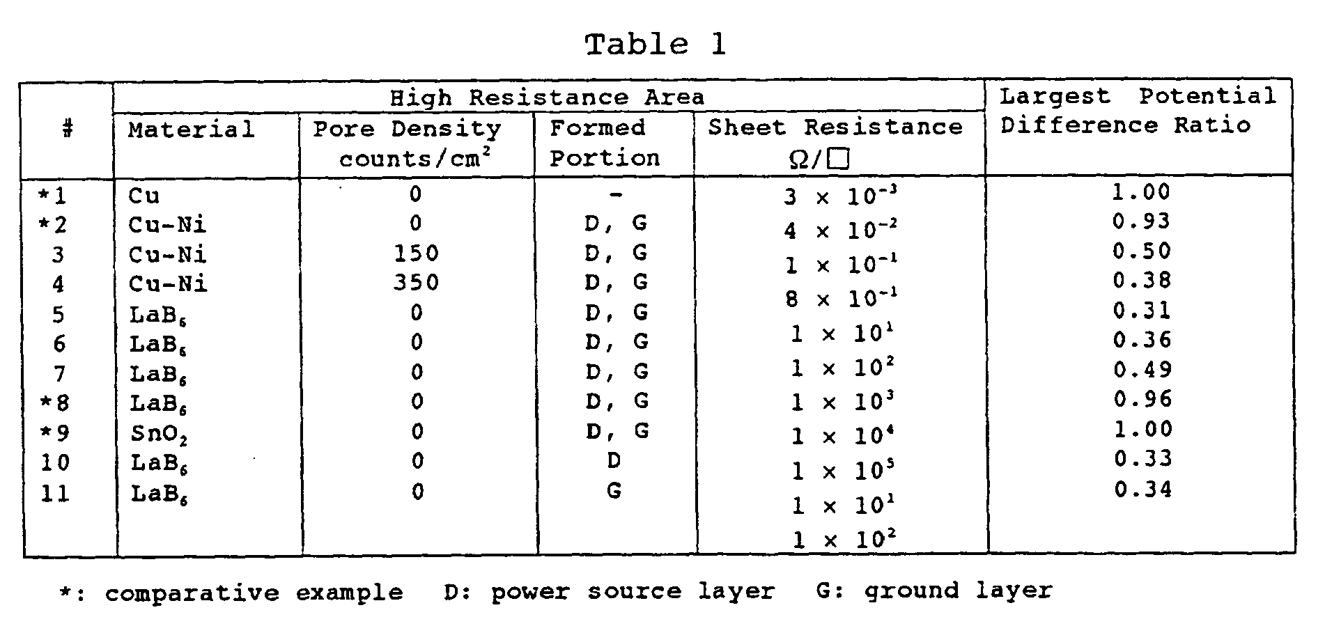
- Table 1 reveals that a ratio of the largest potential difference was maintained as low as 0.5 or below in the wiring boards of
Samples # 3 through #7 andSamples # 10 and #11, in which the high resistance area was formed, whereas a ratio of the largest potential difference was equal to or nearly equal to 1 inSamples # 1, #2, #8, and #9 having a sheet resistance value beyond the range set in the present invention, indicating that considerable variance of voltage had occurred. - In the first example above, the high resistance area having a high resistance with a sheet resistance ranging from 0.1 Ω/□ to 1000 Ω/□ was provided at the peripheral portion of the power source layer and/or ground layer as the method of controlling variance of voltage and a resident wave developed across the power source layer and ground layer within the dielectric substrate.
- The above sheet resistance control is applicable when removing noises at frequencies lower than 1 GHz. However, in a frequency band for frequencies as high as 1 GHz or over, particularly in the microwave frequency band or millimeter frequency band, a current flows near the interface between the conductor and dielectric substrate (skin effect), and the effective resistance becomes higher than a volume resistivity. This makes the effect of the sheet resistance control unsatisfactory in some cases.
- Therefore, in a second example, the
low resistance area 5a of thepower source layer 5, thelow resistance area 6a of theground layer 6, thehigh resistance area 5b of thepower source layer 5, and thehigh resistance area 6b of theground layer 6 are evaluated not by the sheet resistance but by conductivity (unit Ω-1·m-1=S/m). - The following description will describe the second example with reference to Figs. 1 through 5.
- In the arrangement shown in Figs. 1 and 2, the periphery of interior
high conductivity areas power source layer 5 andground layer 6 are surrounded respectively bylow conductivity areas - The high conductivity area a of the
power source layer 5 andground layer 6 is made of conductors, such as Cu, W, and Mo, which have been typically used as conductor materials for the wiring board. In order to lessen a voltage drop due to a conductor loss, a higher conductivity is more preferable, and a desirable conductivity is 1.0 × 10⁷ Ω-1·m-1 or greater. Also, a roughness on the interface between the conductor layer (high conductivity area a) anddielectric substrate 2 is preferably 0 .5 µm or smaller, and most preferably 0.1 µm or smaller, because a too rough surface increases a resistance to high frequencies. - On the other hand, the conductivity in the low conductivity area b is preferably in a range from 70 Ω-1·m-1 to 5 × 10⁶ Ω-1·m-1. This is because when the conductivity in the low conductivity area b is 5 × 10⁶ Ω-1·m-1 or greater, high frequency current absorbing performance becomes too poor, whereas when the conductivity in the low conductivity area b is 70 Ω-1·m-1 or smaller, a high frequency current is not absorbed but reflected. The high frequency current absorbing effect is great when the conductivity is in a range from 100 Ω-1·m-1 to 1 × 10⁴ Ω-1.m-1, in particular.
- Generally, the skin resistance in the high frequency range of 1 GHz or over varies with the surface roughness of the conductor. This is because a current flows near the surface of the conductor when the frequency is high, and the path a high frequency signal travels is extended with an increasing surface roughness of the conductor, thereby increasing a resistance. For example, when the surface roughness is three times as great as the skin depth, the skin resistance is increased by approximately two times. In case of copper, the skin depth is approximately 0.7 µm for a signal of 10 GHz, and if the surface roughness is set to 2 µm or greater, the skin resistance is increased by approximately two times.
- Thus, the high frequency noises can be attenuated by increasing the roughness on the interface between the low conductivity area b and
dielectric substrate 2 by two or more times, in particular, by three or more times as great as the skin depth at the highest frequency of a signal transmitted to the wiring board. - The skin depth referred to herein means a parameter that represents a depth at which the intensity of the magnetic field within the conductor reaches 0.368 (1/e) of a value on the interface of the conductor, and is generally expressed by Equation (1):

- where δ: skin depth
- ω: angular frequency (ω=2πf)
- f: frequency
- µ: magnetic permeability
- σ: conductivity.
- When arranged in the above manner, a high frequency current produced in the
semiconductor device 4 propagates from thecurrent terminal 4a andground terminal 4b to thehigh conductivity area 5a of thepower source layer 5 and thehigh conductivity area 6a of theground layer 6, and is absorbed in the low conductivity area b of thepower source layer 5 andground layer 6. Therefore, neither resonance occurs nor a resident wave is generated in thepower source layer 5 andground layer 6, and as a consequence, it is possible to maintain variance of voltage small while reducing irradiation noises. - A method of adding inorganic powder to the conductor layer forming the low conductivity area b is suitable in forming the low conductivity area b. A quantity of the inorganic powder is preferably 10 percent by weight or more based on the total weight. Inorganic powder composed of constituents similar to or identical with those forming the dielectric substrate is suitable in terms of adhesion or the like.
- A concrete method of forming the low conductivity area is as follows.
- In case that the dielectric substrate is made of ceramic, such as alumina and glass ceramic, powder of raw materials of the foregoing is made into a green sheet by a known sheet forming technique, such as the doctor blade technique.
- Then, the interface between the conductor layer and dielectric substrate is made rough by pressing a panel with rough surface finishing against the green sheet at portions that will be made into the peripheral portions of the ground layer and power source layer, or by scattering coarse ceramic powder composed of the same constituents as those of the dielectric substrate at the peripheral portions of the green sheet, and then applying conductor paste on the area processed by either of the foregoing by means of print coating.
- Also, coarse ceramic powder composed of the major constituent of the dielectric substrate or the constituents same as those of the dielectric substrate is added to the conductor paste, and the resulting conductor paste is applied to the portion forming the low conductivity area b by means of print coating. A quantity of added ceramic powder is preferably 10 percent by weight or more based on the total weight of the conductor paste.
- Alternatively, the conductivity in the low conductivity area b can be adjusted by selecting the conducting materials besides the above-described ceramic powder adding method. Examples of a conductor material having a low conductivity include: a low conductivity material principally composed of at least one of SnO2 and LaB6; and conductor material composed of at least one kind of conductor selected from Cu, W, and Mo with a content of Re, Ru, or a dielectric material. Consequently, it is possible to lower the conductivity in the low conductivity area b.
- Further, modifying the arrangement of the low conductivity area b can lower the conductivity therein.
- For example, an apparent conductivity in the low conductivity area b can be lowered by providing a plurality of
pores 8 as shown in Fig. 3A, providing a plurality ofgrooves 9 as show in Fig. 3B, or scatteringresistors 10 as shown in Fig. 3C. The conductivity can be adjusted depending on the size or number of thepores 8,grooves 9, andresistors 10. - Also, the width of the peripheral portion of the low conductivity area b is preferably 0.1 mm or greater. This is because when the width of the low conductivity area b is too small, not only the manufacturing becomes difficult, but also the effect of absorbing a high frequency current is lessened. The upper limit of the width of the low conductivity area b is not especially imposed as long as a sufficient area can be secured for the high conductivity area a. It should be noted, however, that the effect is substantially the same from the point the width exceeds 30 mm.
- As to an arrangement of a connected portion of the high conductivity area a and low conductivity area b, in case that these areas are made of totally different conductor materials, an arrangement as shown in Fig. 4B or 4C such that places a conductor material al forming the high conductivity area a and a conductor material bl forming the low conductivity area b to overlap is preferable compared with an arrangement as shown in Fig. 4A such that places the high conductivity area a and low conductivity area b not to overlap at all. Also, in case that the
power source layer 5 andground layer 6 are formed on the surface layer of the wiring board, the conductor material bl forming the low conductivity area b may cover the conductor material al forming the high conductivity area a entirely as shown in Fig. 4D. In the arrangement shown in Fig. 4D, a current flows through the high conductivity area a at the side touching thedielectric substrate 2, which prevents the conductivity from dropping. - Further, as shown in Fig. 4E, in case that the
power source layer 5 andground layer 6 are formed within the substrate, it may be arranged such that the high conductivity area a is formed on the respective opposing surfaces of thepower source layer 5 andground layer 6, and the low conductivity area b is formed to cover the area a entirely. In this case, the viaconductor 7 must be provided so as to be connected to the high conductivity area a. - Figs. 5A through 5C are views showing other concrete examples of the power source layer and ground layer in the wiring board.
- As shown in Fig. 5A, it may be arranged such that the
power source layer 5 andground layer 6 are separated into a plurality of areas, and the low conductivity area b is formed at the periphery of each high conductivity area a. As shown in Fig. 5B, the low conductivity area b may be formed at the periphery of the high conductivity area a at regular intervals x. In this case, a noise absorption quantity is reduced with an increasing ratio of the interval x with respect to the length of the periphery, and for this reason, a sum of the intervals x is preferably 1/3 or less of the overall length of the periphery. - In addition, as shown in Fig. 5C, the low conductivity area b may be composed of areas bl through b3 each having a different conductivity. In this case, given σa as the conductivity in the high conductivity area a, and σb1, σb2, and σb3 as the conductivities in the areas b1, b2, and b3, respectively, then it is preferable to arrange such that the conductivities from inside to outside satisfy the following inequality relation: σa>σb1>σb2>σb3. Also, each of the areas b1, b2, and b3 can be arranged in such a manner that the conductivity varies continuously from inside to outside.
- Further, the surface of the
dielectric substrate 2 in the low conductivity area b can be of a repeating shape, such as a rectangle as shown in Fig. 7A, a triangle as shown in Fig. 7B, and a rounded shape as shown in Fig. 7C, or an irregular concave and convex pattern as shown in Fig. 7D when the inorganic power is added to the conductor layer. - A material of the
dielectric substrate 2, and materials of thewiring circuit layer 3 and viaconductors 7 can be the same as those used in the first embodiment. - The following description will describe in detail an example of a wiring board with reference to Figs. 8A and 8B. In the wiring board of the present example, an alumina sintered body was used as a
dielectric substrate 11. Initially, slurry was prepared by adding with blending an organic binder, a plasticizer, and a solvent to mixed power of Al2O3) having an average particle size of 0.2 µm added with 7 percent by weight of a sintering assistant including SiO2, MgO, and CaO based on the total weight. Then, the known doctor blade technique was applied to the slurry, whereby a ceramic green sheet of approximately 250 µm thick was formed. Subsequently, a via 13 was made at a position used as an excitation position by providing a through hole in the ceramic green sheet by the perforating technique. - Adequate organic binder, plasticizer, solvent, etc. were added to a powder raw material principally composed of tungsten (W) with blending, whereby metal paste was obtained. The metal paste thus obtained was filled in a through hole portion in the ceramic green sheet by means of printing, and applied as well on the surface of a through hole forming portion to be shaped into a
power source terminal 14 by means of print coating. - Then, the green sheet that had undergone print coating was calcined in a reducing atmosphere of a mixed gas of hydrogen (H2) and nitrogen (N2) at 1600°C, whereby an alumina substrate having the length of 56 mm, width of 80 mm, and thickness of 250 µm was obtained.
- Subsequently, a
ground layer 15 was formed on the main surface of the alumina substrate and apower source layer 12 was formed on the back surface of the same by the following methods. A constant width of 4 mm was given when the low conductivity area b was formed. Then,Samples # 1 through #10 were obtained in the following manner. - In
Sample # 1, both theground layer 15 andpower source layer 12 were formed out of Cu paste by means of print coating without forming the low conductivity area, and baked at 900°C. - In
Samples # 2 through #10, ahigh conductivity area 15a of theground layer 15 and ahigh conductivity area 12a of thepower source layer 12 were formed out of Cu paste by means of print coating, and baked at 900°C. Here, as shown in Fig. 8B, the print coating was omitted at and around thepower source terminal 14 pre-formed out of tungsten in thehigh conductivity area 15a of theground layer 15. Subsequently, metal paste prepared by adding an alumina constituent to Cu, Cu-W, Cu-Ni, or LaB6 as necessary in a ratio set forth in Table 2 below was printed at the periphery of thehigh conductivity areas ground layer 15 andpower source layer 12, respectively in such a manner so as to overlap thehigh conductivity areas low conductivity areas - Also, in
Samples # 4 through #10, the surface of the dielectric substrate was made rough mechanically by pressing a panel with rough surface finishing against the dielectric substrate at portions to be made into thelow conductivity areas - Further, in
Sample # 8, the low conductivity area was formed in the power source layer (D) alone, and inSample # 9, the low conductivity area was formed in the ground layer (G) alone. - The tip of a
wafer probe 18 was brought into contact with thepower source terminal 14 andground terminal 16 provided at excitation positions in the evaluation alumina wiring boards ofSamples # 1 through #10 obtained in the above manner, and a return loss (S11) was measured by a network analyzer in a frequency range from 1 GHz to 40 GHz. Here, Sample having -5 dB or lower in a frequency range from 20 GHz to 30 GHz as the largest value of S11 was judged as effective in controlling variance of voltage. - The roughness (Ra: surface roughness) on the interface between the dielectric substrate and the conductor layer in the low conductivity area was measured by using a BEM (reflection electron image) of a scanning electron microscope. The skin depth was set to 3.4 µm, which was the value of Cu at a frequency of 500 MHz (the highest frequency of a signal transmitted to the wiring board). In Table 2 below, a ratio of the surface roughness and skin depth is set forth in the column of "surface roughness/skin depth".
- The conductivity of the conductor forming the low conductivity area was measured by manufacturing a substrate having a line path with a width of 2 mm and a length of 30 mm on one surface of a 0.2-mm-thick dielectric layer, and measuring a resistance value of the line path by a 4-terminal measuring method. The thickness of the line path was measured by observing the cross section with a metallurgical microscope.
Table 2 # Low Conductivity Area Material Surface Roughness/ Skin Depth Surface Finishing Press Inorganic Materials Added to Conductor Layer wt% Formed Portion Conductivity Ω-1m-1 S11 dB *1 Cu 0.95 X 3 - 3.0×10⁷ -1.21 *2 Cu 1.64 X 8 D, G 1.7×10⁷ -3.28 *3 Cu-W 0.68 X 3 D, G 4.7×10⁶ -4.71 4 Cu-W 2.73 O 8 D, G 4.7×10⁶ -5.02 5 Cu-W 2.23 O 20 D, G 4.4×10⁶ -6.42 6 Cu-Ni 2.11 O 20 D, G 8.8×10⁵ -8.02 7 LaB6 2.58 O 20 D, G 4.8×10³ -13.56 8 LaB6 2.74 O 20 D 5.3×10³ -12.39 9 LaB6 2.71 O 20 G 5.1×10² -8.39 *10 LaB6 2.41 O 20 D, G 5.1×101 -4.62 *: comparative example D: power source layer G: ground layer - Table 2 reveals that the return loss S11 was attenuated by 5 dB or more in
Samples # 4 through #9, in which the low conductivity area was formed, indicating that the effect of the present invention was achieved. - On the contrarily, the return loss was less than 5 dB in
Sample # 1, in which the low conductivity area was not formed. - Also, even when the conductivity in the low conductivity area was in an adequate range, a satisfactory effect was not achieved if the "surface roughness/skin depth" is smaller than two times like in
Samples # 2 and #3, and if the conductivity in the low conductivity area was too low like inSample # 10. In view of the foregoing, it is understood that it is necessary to set the above ratio to two or more times in a high frequency range from 1 to 40 GHz. - The following description will describe a concrete arrangement according to an embodiment of the present invention with reference to the accompanying drawings.
- Fig. 9 is a cross section of a wiring board, and Fig. 10 is a view showing a pattern of a power source layer in the wiring board of Fig. 9.
- In a
wiring board 1 shown in Fig. 9, awiring circuit layer 3 for signal transmission is formed on the surface of adielectric substrate 2, and asemiconductor device 4 serving as a digitally operating electronic component, such as a C-MOS integrated circuit, is mounted on the surface of thewiring board 1 and connected to thewiring circuit layer 3 provided on the surface (this connection state is not illustrated).Numeral 21 denotes an input/output terminal. - In addition, a
power source layer 5 and aground layer 6 are formed within thedielectric substrate 2. Apower source terminal 4a and aground terminal 4b of thesemiconductor device 4 are electrically connected to thepower source layer 5 andground layer 6, respectively through viaconductors 7 provided through thedielectric substrate 2. - According to the present invention, as shown in Fig. 10, major characteristics are that the
power source layer 5 and/orground layer 6 are separated into an area A including at least aconnection 7a to the viaconductor 7 serving as a connecting body and an area B of the rest by a high impedance strip C. In the drawing, a first area A (hereinafter, referred to simply as the "area A") connected to a digitally operating electronic component is formed near the center of thewiring board 1, and a second area B (hereinafter, referred to simply as the "area B") is formed at both sides of the area A in such a manner that the input/output terminal 21 is connected to or provided in the vicinity of the area B. A high impedance strip C is provided between these areas A and B. - According to the above arrangement, when attention is focused on the
power source layer 5, for example, a high frequency current produced in thesemiconductor device 4 propagates to the area A of thepower source layer 5 through thepower source terminal 4a and viaconductor 7 and is absorbed and attenuated in the high impedance strip C provided to surround the area A. This makes it possible to control variance of potential of thepower source layer 5 andground layer 6 in the area B connected to the input/output terminal 21, thereby reducing irradiation noises from the input/output terminal 21, a cable, or the like. - As shown in Fig. 10, the high impedance strip C is composed of a high resistance strip C1 and a low resistance strip C2. It is preferable to shape the high resistance strip C1 comb-wise or in spirals in order to effectively absorb and attenuate high frequency noises in a hard-to-absorb mode. Also, it is preferable to shape the low resistance strip C2 in meanders (fanfolds, zigzags) or spirals.
- In addition, the high resistance strip C1 is provided at the entire peripheral portion of the
power source layer 5. - By shaping the high resistance strip C1 comb-wise or in spirals, the low resistance strip C2 formed between the high resistance strips C1 is shaped in meanders or spirals. This gives rise to a large inductance component and makes it difficult for high frequency noises to propagate from the area A to the area B. As a consequence, it is possible to control variance of voltage in the area B markedly.
- Although the areas A and B are separated by the high impedance strip C in terms of high frequencies, a connection is established therebetween by the low resistance strip C2 forming the high impedance strip C to allow a direct current or low frequency current to pass through.
- The
power source layer 5,ground layer 6, and the low resistance strip C2 forming the high impedance strip C are preferably made of conductor materials principally composed of at least one kind of element selected from Cu, W, and Mo, for example, which are generally used as conductor materials. - On the other hand, the high resistance strip C1 in the high impedance strip C has a relatively high sheet resistance in comparison with the conductor materials forming the low resistance strip C2 and the other components including the
power source layer 5 andground layer 6. Given R1 as the sheet resistance of the conductor material forming the areas A and B, and R2 as the sheet resistance in the high resistance strip C1, then it is preferable that a sheet resistance difference R2-R1 is 0.08 Ω/□ or greater, and in particular, 0.48 Ω/□ or greater. - In particular, it is preferable that the sheet resistance value of the high resistance strip C1 is in a range from 0.01 Ω/□ to 10000 Ω/□. This is because when the sheet resistance in the high resistance strip C1 is lower than 0.01 Ω/□, noise absorbing and attenuating performance becomes too poor to form the high impedance strip C, whereas when the sheet resistance in the high resistance strip C1 exceeds 10000 Ω/□, noises are not absorbed but reflected. Particularly, the most suitable range of the sheet resistance value of the high resistance strip C1 is from 0.5 Ω/□ to 100 Ω/□.
- In the present invention, forming the high resistance strip C1 out of a conductor material having a higher resistance than that of the low resistance strip C2 is preferable as a concrete method of forming the high resistance strip C1. Examples of such a conductor material having a higher resistance include a resistor material principally composed of at least one of SnO2 and LaB6, and a conductor material made of at least one kind of conductor selected from Cu, W, and Mo with a content of at least one element selected from the group consisting of Re, Ru, and a dielectric material.
- Also, the strip width of the high resistance strip C1 forming the high impedance strip C is preferably 0.1 mm or greater. This is because when the width of the high resistance strip C1 is too small, not only the manufacturing becomes difficult, but also the effect of reducing noises is lessened. The upper limit of the strip width of the high resistance strip C1 is not especially imposed as long as the areas A and B can be secured. It should be noted, however, that the effect is substantially the same from the point the strip width exceeds 30 mm.
- The high resistance strip C1 in the high impedance strip C is formed continuously with the low resistance strip C2 and the areas A and B of the
power source layer 5 andground layer 6 so as to be electrically connected. - Figs. 11 through 15 are views showing other concrete embodiments of the
power source player 5. - Fig. 11 shows a pattern where the high impedance strip that is provided at the entire peripheral portion of the
power source layer 5 in the pattern shown in Figs. 9 and 10 is omitted. - Fig. 12 is a view showing a pattern where the areas A and B are separated by forming the area A having the
connection 7a to the digital operating electronic component at the left side of the board, the area B connected to the input/output terminal at the right side, and the high impedance strip C at the center. The high resistance strip C1 in the high impedance strip C is shaped comb-wise, and the areas A and B are connected to each other by the low resistance strip C2 shaped in meanders and provided between the comb-wise high resistance strips C1. - Fig. 13 is a view showing a pattern where the areas A and B are separated by forming the area A having the
connection 7a to the digitally operating electronic component at the center of the board, the area B connected to the input/output terminal above and below the area A, and the high impedance strip C at the top and bottom of the area A. The high resistance strip C1 in the high impedance strip C is shaped comb-wise, and the areas A and B are connected to each other by the low resistance strip C2 shaped in meanders and provided between the comb-wise high resistance strips C1. - Fig. 14 is a view showing a pattern where the areas A and B are separated by forming the area A having the
connection 7a to the digitally operating electronic component at the lower right corner of the board, the area B connected to the input/output terminal at the rest of the board, and the high impedance strip C to encircle the lower right corner area. The high resistance strip C1 in the high impedance strip C is shaped comb-wise, and the areas A and B are connected to each other by the low resistance strip C2 shaped in meanders and provided between the comb-wise high resistance strips C1. - Fig. 15 is a view showing a pattern where the
connection 7a to the digitally operating electronic component is provided to the board at two positions, 7a1 and 7a2, and an area A1 having the connection 7a1, an area A2 having the connection 7a2, and an area B connected to the input/output terminal are placed. Here, the two areas A1 and A2 are separated from the area B by forming the high impedance strip C to surround the two connections 7a1 and 7a2. - In the area A1, the high resistance strip C1 in the high impedance strip C is shaped comb-wise, and the areas A1 and B are connected to each other by the low resistance strip C2 shaped in meanders and provided between the comb-wise high resistance strips C1. In the area A2, the high resistance strip C1 in the high impedance strip C is shaped in spirals, and the areas A2 and B are connected to each other by the low resistance strip C2 shaped in spirals.
- Examples of materials forming the
dielectric substrate 2 include dielectric materials containing a dielectric substrate principally composed of alumina (Al2O3), ceramic principally composed of aluminum nitride (AlN), silicon nitride (Si3N4),silicon carbide (SiC), mullite (3Al2O3·2SiO2), glass ceramic, etc., and organic resin, such as epoxy resin and glass-epoxy composite, imide resin, amide-imide resin and resin-ceramic composite. - Also, the
wiring circuit layer 3 and viaconductors 7 can be made of materials, such as Cu, W, and Mo, or alloy including the foregoing. - The following description will describe in detail an example of the wiring board of the present invention with reference to Figs. 16A and 16B.
- In the wiring board of the present example, an alumina sintered body was used as a
dielectric substrate 11. Initially, slurry was prepared by adding with blending an organic binder, a plasticizer, and a solvent to mixed power of Al2O3 powder added with 7 percent by weight of a sintering assistant including SiO2, MgO, and CaO based on the total weight. The known doctor blade technique was applied to the slurry, whereby a ceramic green sheet of approximately 300 µm thick was formed. Then, a via 13 was made at a position used as an excitation position by providing a through hole in the ceramic green sheet by a micro-drill. - Adequate organic binder, plasticizer, solvent, etc. were added to a powder raw material principally composed of tungsten (W) with blending, whereby metal paste was obtained. The metal paste thus obtained was filled in a through hole portion in the ceramic green sheet and applied as well by means of print coating.
- Then, the green sheet was calcined in a reducing atmosphere of a mixed gas of hydrogen (H2) and nitrogen (N2) at approximately 1600°C, whereby an alumina wiring board having the length of 56 mm, width of 80 mm, and thickness of 250 µm was obtained.
- A
ground layer 15 was formed on the main surface of the alumina wiring board and apower source layer 12 was formed on the back surface of the same. Here, on the assumption that an area A connected to a digitally operating electronic component was formed at the center of the board and an area B connected to an input/output terminal was formed above and below the area A, a high impedance strip C was formed at the top and bottom of the area A. In the high impedance strip C, the high resistance strip C1 was formed in spirals. A constant width of 3 mm was given as the strip width of the high resistance strip C1 in the high impedance stripC. Samples # 1 through #11 were obtained in the above manner. - In
Sample # 1, both theground layer 15 andpower source layer 12 were formed out of Cu paste by means of print coating without forming the high impedance strip, and baked at 900°C. - In
Samples # 2 through #11, the areas A and B, and the low resistance strip C2 in the high impedance strip C were formed out of Cu paste by means of print coating in accordance with the pattern shown in Fig. 16C, and baked at 900°C. Here, in theground layer 15, the print coating was omitted at and around thepower source terminal 14 connected to the viaconductor 13 as shown in Fig. 16A, and theground layer 15 was baked at 900°C. Subsequently, resistor paste containing Cu-Ni, LaB6, or SnO2 was printed on thepower source layer 12 in such a manner that the pattern of the high resistance strip C1 shown in Fig. 16C overlaps the low resistance strip C2, and the layer was baked at 900°C, whereby the high resistance strip C1 was formed. - In
Sample # 10, the high impedance strip was formed in the same pattern in both the power source layer (D) and ground layer (G), and inSample # 11, the high impedance strip was formed in the ground layer (G) alone and the power source layer was provided with the conductor (Cu) pattern alone. - Then, the
central axis 17a of acoaxial cable 17 was fixedly connected to thepower source terminal 14 bysolder 19, which was provided at the excitation point in each wiring board obtained in the above manner. Also, aground tube 17b of the coaxial cable was fixedly connected to aground terminal 16 provided inside theground layer 15 by thesolder 19. - A sine wave of 30 MHz to 1000 MHz was inputted from the coaxial cable to each wiring board thus manufactured, and a largest potential difference in a frequency range from 30 MHz to 1000 MHz was measured by bringing a high impedance measuring probe into contact with the area B of the
ground layer 15 at a position where variance of voltage reached its maximum. Then, a ratio of the largest potential difference in each wiring board on a base of 1 with reference to the largest potential difference inSample # 1 having no high impedance strip was measured and the result is set forth in Table 3 below.
- In comparison with
Sample # 1, in which the high impedance strip was not formed, a ratio of the largest potential difference was lessened inSamples # 2 through #11, in which the high impedance strip was formed. In particular, a ratio of the largest potential difference was maintained as low as 0.5 or less with the wiring boards ofSamples # 3 through #7, andSamples # 10 and #11, in which the high resistance strip in the high impedance strip had a sheet resistance ranging from 0.1 Ω/□ to 1000 Ω/□.
Claims (7)
- A wiring board (1), on which an electronic component (4) is mounted, comprising:a dielectric substrate (2; 11);a wiring circuit layer (3) formed on a main surface and/or a back surface of said dielectric substrate (2);a power source layer (5; 12) formed on a main surface and/or a back surface of said dielectric substrate (2; 11), and/or within said dielectric substrate (2; 11);a ground layer (6; 15) formed on the main surface and/or back surface of said dielectric substrate (2; 11), and/or within said dielectric substrate (2; 11); anda connector (7; 13, 14) for electrically connecting said electronic component (4) and power source layer (5; 12), and said electronic component (4) and ground layer (6; 15),said wiring board (1) being characterized in that:either or both of said power source layer (5; 12) and ground layer (6; 15) are separated into a first area (A) and a second area (B) by a high impedance strip (C); andsaid first area (A) includes a connection (7a) to said connector (7),said high impedance strip (C) is composed of a high resistance strip (C1) and a low resistance strip (C2),the sheet resistance value R2 of said high resistance strip (C1) is in a range from 0.01 Ω/□ to 10000 Ω/□,a sheet resistance difference R2-R1 between the sheet resistance R1 of the conductor material forming the first area (A) and the second area (B), and the sheet resistance R2 in the high resistance strip (C1) is 0.08 Ω/□ or greater.
- The wiring board of claim 1, characterized in that said high resistance strip (C1) is shaped comb-wise or in spirals.
- The wiring board of claim 1, characterized in that said low resistance strip (C2) is shaped in meanders or spirals.
- The wiring board of any of claims 1-3, characterized in that said power source layer (5; 12) and/or ground layer (6; 15) are made of a conductor material principally composed of at least one kind of element selected from Cu, W, and Mo.
- The wiring board of any of claims 1-4, characterized in that said high resistance strip (C1) is made of a resistor material principally composed of at least one of SnO2 and LaB6, or a conductor material composed of at least one kind of conductor selected from Cu, W, and Mo with a content of at least one kind of element selected from Re, Ru, and a dielectric material.
- The wiring board of any of claims 1-5, characterized in that a high frequency circuit is connected to either of said first area (A) and second area (B), and a low frequency circuit is connected to the other.
- The wiring board of claim 1, characterized in that said two areas (A, B) separated by said high impedance strip (C) are connected to each other through said low resistance strip (C2) to allow a direct current or low frequency current to pass through.
Applications Claiming Priority (4)
| Application Number | Priority Date | Filing Date | Title |
|---|---|---|---|
| JP2000053997A JP3652203B2 (en) | 2000-02-29 | 2000-02-29 | Wiring board |
| JP2000053997 | 2000-02-29 | ||
| JP2000130989 | 2000-04-28 | ||
| JP2000130989A JP3615688B2 (en) | 2000-04-28 | 2000-04-28 | Wiring board |
Publications (3)
| Publication Number | Publication Date |
|---|---|
| EP1130950A2 EP1130950A2 (en) | 2001-09-05 |
| EP1130950A3 EP1130950A3 (en) | 2003-12-17 |
| EP1130950B1 true EP1130950B1 (en) | 2007-11-21 |
Family
ID=26586394
Family Applications (1)
| Application Number | Title | Priority Date | Filing Date |
|---|---|---|---|
| EP01104820A Expired - Lifetime EP1130950B1 (en) | 2000-02-29 | 2001-02-27 | Wiring board |
Country Status (3)
| Country | Link |
|---|---|
| US (1) | US6469259B2 (en) |
| EP (1) | EP1130950B1 (en) |
| DE (1) | DE60131485T2 (en) |
Families Citing this family (20)
| Publication number | Priority date | Publication date | Assignee | Title |
|---|---|---|---|---|
| DE19907542C2 (en) * | 1999-02-22 | 2003-07-31 | Vacuumschmelze Gmbh | Flat magnetic core |
| AU2002308354A1 (en) * | 2001-03-08 | 2002-09-24 | Ilfa Industrieelektronik Und Leiterplattenfertigung Aller Art Gmbh | Multilayer printed circuit board |
| JP3531621B2 (en) * | 2001-04-12 | 2004-05-31 | 日本電気株式会社 | Portable wireless devices |
| US20030042044A1 (en) * | 2001-08-30 | 2003-03-06 | Micron Technology, Inc. | Circuit board plane interleave apparatus and method |
| JP2003283086A (en) * | 2002-01-21 | 2003-10-03 | Hitachi Cable Ltd | Wiring board, method of manufacturing wiring board, and electronic component using wiring board |
| WO2004077906A1 (en) * | 2003-02-28 | 2004-09-10 | Wireless Lan Systems Oy | A circuit board and arrangement for minimizing thermal and electromagnetic effects |
| JP4101156B2 (en) * | 2003-11-05 | 2008-06-18 | シャープ株式会社 | Circuit board |
| US7508062B2 (en) * | 2005-03-11 | 2009-03-24 | Lsi Corporation | Package configuration and manufacturing method enabling the addition of decoupling capacitors to standard package designs |
| WO2006130632A2 (en) * | 2005-05-31 | 2006-12-07 | Invitrogen Corporation | Separation and purification of nucleic acid from paraffin-containing samples |
| US8134084B2 (en) | 2006-06-30 | 2012-03-13 | Shin-Etsu Polymer Co., Ltd. | Noise-suppressing wiring-member and printed wiring board |
| WO2008018870A1 (en) * | 2006-08-09 | 2008-02-14 | Geomat Insights, Llc | Integral charge storage basement and wideband embedded decoupling structure for integrated circuit |
| JP5165912B2 (en) * | 2007-03-15 | 2013-03-21 | 株式会社日立製作所 | Low noise semiconductor device |
| WO2011114944A1 (en) * | 2010-03-15 | 2011-09-22 | 日本電気株式会社 | Noise suppression structure |
| JP5088427B2 (en) * | 2011-03-02 | 2012-12-05 | 第一精工株式会社 | Electrical connector and electrical connector assembly |
| TW201316895A (en) * | 2011-10-14 | 2013-04-16 | Hon Hai Prec Ind Co Ltd | Printed circuit board capable of preventing electromagnetic interface |
| CN107318215A (en) * | 2016-04-26 | 2017-11-03 | 鸿富锦精密电子(天津)有限公司 | The electronic installation of printed circuit board (PCB) and the application printed circuit board (PCB) |
| JP6735185B2 (en) * | 2016-08-25 | 2020-08-05 | 京セラ株式会社 | Multilayer wiring board and electronic device |
| JP6519630B1 (en) * | 2017-10-30 | 2019-05-29 | ダイキン工業株式会社 | Current detection device |
| US11259403B1 (en) * | 2020-10-30 | 2022-02-22 | SK Hynix Inc. | Printed circuit board structure for solid state drives |
| CN113194599B (en) * | 2021-04-23 | 2022-05-03 | 四川九洲电器集团有限责任公司 | Integrated integration method based on multifunctional composite substrate |
Citations (1)
| Publication number | Priority date | Publication date | Assignee | Title |
|---|---|---|---|---|
| US5898576A (en) * | 1996-11-12 | 1999-04-27 | Bay Networks Inc. | Printed circuit board including a terminated power plane and method of manufacturing the same |
Family Cites Families (8)
| Publication number | Priority date | Publication date | Assignee | Title |
|---|---|---|---|---|
| JP3090453B2 (en) * | 1989-07-10 | 2000-09-18 | 株式会社日立製作所 | Thick film thin film laminated substrate and electronic circuit device using the same |
| JPH09205290A (en) * | 1996-01-24 | 1997-08-05 | Hitachi Ltd | Circuit board having low EMI structure |
| JPH09266361A (en) * | 1996-03-28 | 1997-10-07 | Oki Electric Ind Co Ltd | Voltage variation accommodating structure of circuit board |
| JPH10126014A (en) * | 1996-10-23 | 1998-05-15 | Sony Corp | Circuit board |
| JP3926880B2 (en) * | 1997-03-31 | 2007-06-06 | 富士通株式会社 | Multilayer printed board |
| US6181571B1 (en) * | 1998-03-06 | 2001-01-30 | Canon Kabushiki Kaisha | Printed-wiring board and electronic device having the same wiring board |
| JP4260243B2 (en) * | 1998-05-25 | 2009-04-30 | 三菱電機株式会社 | Laminated printed wiring board |
| US6137064A (en) * | 1999-06-11 | 2000-10-24 | Teradyne, Inc. | Split via surface mount connector and related techniques |
-
2001
- 2001-02-27 EP EP01104820A patent/EP1130950B1/en not_active Expired - Lifetime
- 2001-02-27 DE DE60131485T patent/DE60131485T2/en not_active Expired - Lifetime
- 2001-02-27 US US09/795,765 patent/US6469259B2/en not_active Expired - Fee Related
Patent Citations (1)
| Publication number | Priority date | Publication date | Assignee | Title |
|---|---|---|---|---|
| US5898576A (en) * | 1996-11-12 | 1999-04-27 | Bay Networks Inc. | Printed circuit board including a terminated power plane and method of manufacturing the same |
Also Published As
| Publication number | Publication date |
|---|---|
| EP1130950A2 (en) | 2001-09-05 |
| DE60131485T2 (en) | 2008-10-09 |
| US20010050182A1 (en) | 2001-12-13 |
| DE60131485D1 (en) | 2008-01-03 |
| US6469259B2 (en) | 2002-10-22 |
| EP1130950A3 (en) | 2003-12-17 |
Similar Documents
| Publication | Publication Date | Title |
|---|---|---|
| US6469259B2 (en) | Wiring board | |
| JP2003283073A (en) | Wiring board | |
| US6936921B2 (en) | High-frequency package | |
| JP3652203B2 (en) | Wiring board | |
| JP4462782B2 (en) | High frequency wiring board | |
| JP3987664B2 (en) | Wiring board | |
| JP2001016007A (en) | Wiring board with transmission line | |
| JP2003283148A (en) | Wiring board | |
| JPH08228105A (en) | Microstrip substrate | |
| JP2000077852A (en) | Wiring board | |
| JP3825350B2 (en) | Ceramic wiring board | |
| JP3615688B2 (en) | Wiring board | |
| JPH0878912A (en) | Multilayer circuit board with stripline | |
| JP3784185B2 (en) | Wiring board for mounting electronic components | |
| JP2003031956A (en) | Ceramic wiring board and method of manufacturing the same | |
| JP3784188B2 (en) | Wiring board for mounting electronic components | |
| JP4518664B2 (en) | Wiring board mounting structure and semiconductor device | |
| Tagami et al. | Glass ceramics functional substrate development | |
| JP2003198213A (en) | High frequency wiring board | |
| JPH06291521A (en) | High frequency multi-layer integrated circuit | |
| JP2003046238A (en) | Ceramic wiring board and method of manufacturing the same | |
| JP2001068852A (en) | Multilayer wiring board and method of manufacturing the same | |
| JP3921078B2 (en) | Wiring board | |
| JP3535005B2 (en) | High frequency semiconductor package | |
| JP3638528B2 (en) | Package for storing semiconductor elements |
Legal Events
| Date | Code | Title | Description |
|---|---|---|---|
| PUAI | Public reference made under article 153(3) epc to a published international application that has entered the european phase |
Free format text: ORIGINAL CODE: 0009012 |
|
| AK | Designated contracting states |
Kind code of ref document: A2 Designated state(s): AT BE CH CY DE DK ES FI FR GB GR IE IT LI LU MC NL PT SE TR |
|
| AX | Request for extension of the european patent |
Free format text: AL;LT;LV;MK;RO;SI |
|
| PUAL | Search report despatched |
Free format text: ORIGINAL CODE: 0009013 |
|
| AK | Designated contracting states |
Kind code of ref document: A3 Designated state(s): AT BE CH CY DE DK ES FI FR GB GR IE IT LI LU MC NL PT SE TR |
|
| AX | Request for extension of the european patent |
Extension state: AL LT LV MK RO SI |
|
| 17P | Request for examination filed |
Effective date: 20040518 |
|
| 17Q | First examination report despatched |
Effective date: 20040618 |
|
| AKX | Designation fees paid |
Designated state(s): DE FR IT |
|
| GRAP | Despatch of communication of intention to grant a patent |
Free format text: ORIGINAL CODE: EPIDOSNIGR1 |
|
| RIN1 | Information on inventor provided before grant (corrected) |
Inventor name: KAJI, MASAKIC/O KYOCERA CORPORATION Inventor name: TERAO SHINYAC/O KYOCERA CORPORATION Inventor name: KOGA, RYUJI Inventor name: TAKESHITA YOSHIHIROC/O KYOCERA CORPORATION Inventor name: TAKENOUCHI SATORUC/O KYOCERA CORPORATION |
|
| GRAS | Grant fee paid |
Free format text: ORIGINAL CODE: EPIDOSNIGR3 |
|
| GRAA | (expected) grant |
Free format text: ORIGINAL CODE: 0009210 |
|
| AK | Designated contracting states |
Kind code of ref document: B1 Designated state(s): DE FR IT |
|
| REF | Corresponds to: |
Ref document number: 60131485 Country of ref document: DE Date of ref document: 20080103 Kind code of ref document: P |
|
| ET | Fr: translation filed | ||
| PLBE | No opposition filed within time limit |
Free format text: ORIGINAL CODE: 0009261 |
|
| STAA | Information on the status of an ep patent application or granted ep patent |
Free format text: STATUS: NO OPPOSITION FILED WITHIN TIME LIMIT |
|
| 26N | No opposition filed |
Effective date: 20080822 |
|
| PGFP | Annual fee paid to national office [announced via postgrant information from national office to epo] |
Ref country code: FR Payment date: 20110302 Year of fee payment: 11 Ref country code: DE Payment date: 20110323 Year of fee payment: 11 Ref country code: IT Payment date: 20110221 Year of fee payment: 11 |
|
| REG | Reference to a national code |
Ref country code: FR Ref legal event code: ST Effective date: 20121031 |
|
| PG25 | Lapsed in a contracting state [announced via postgrant information from national office to epo] |
Ref country code: IT Free format text: LAPSE BECAUSE OF NON-PAYMENT OF DUE FEES Effective date: 20120227 |
|
| REG | Reference to a national code |
Ref country code: DE Ref legal event code: R119 Ref document number: 60131485 Country of ref document: DE Effective date: 20120901 |
|
| PG25 | Lapsed in a contracting state [announced via postgrant information from national office to epo] |
Ref country code: FR Free format text: LAPSE BECAUSE OF NON-PAYMENT OF DUE FEES Effective date: 20120229 |
|
| PG25 | Lapsed in a contracting state [announced via postgrant information from national office to epo] |
Ref country code: DE Free format text: LAPSE BECAUSE OF NON-PAYMENT OF DUE FEES Effective date: 20120901 |