EP1126475A2 - Verfahren und Vorrichtung zum Testen eines als Arbeitsspeicher im Personal Computer eingesetzten SDRAM-Speichers - Google Patents
Verfahren und Vorrichtung zum Testen eines als Arbeitsspeicher im Personal Computer eingesetzten SDRAM-Speichers Download PDFInfo
- Publication number
- EP1126475A2 EP1126475A2 EP01103000A EP01103000A EP1126475A2 EP 1126475 A2 EP1126475 A2 EP 1126475A2 EP 01103000 A EP01103000 A EP 01103000A EP 01103000 A EP01103000 A EP 01103000A EP 1126475 A2 EP1126475 A2 EP 1126475A2
- Authority
- EP
- European Patent Office
- Prior art keywords
- memory
- sdram
- test mode
- test
- activating
- Prior art date
- Legal status (The legal status is an assumption and is not a legal conclusion. Google has not performed a legal analysis and makes no representation as to the accuracy of the status listed.)
- Withdrawn
Links
Images


Classifications
-
- G—PHYSICS
- G11—INFORMATION STORAGE
- G11C—STATIC STORES
- G11C29/00—Checking stores for correct operation ; Subsequent repair; Testing stores during standby or offline operation
- G11C29/56—External testing equipment for static stores, e.g. automatic test equipment [ATE]; Interfaces therefor
-
- G—PHYSICS
- G11—INFORMATION STORAGE
- G11C—STATIC STORES
- G11C11/00—Digital stores characterised by the use of particular electric or magnetic storage elements; Storage elements therefor
- G11C11/21—Digital stores characterised by the use of particular electric or magnetic storage elements; Storage elements therefor using electric elements
- G11C11/34—Digital stores characterised by the use of particular electric or magnetic storage elements; Storage elements therefor using electric elements using semiconductor devices
- G11C11/40—Digital stores characterised by the use of particular electric or magnetic storage elements; Storage elements therefor using electric elements using semiconductor devices using transistors
- G11C11/401—Digital stores characterised by the use of particular electric or magnetic storage elements; Storage elements therefor using electric elements using semiconductor devices using transistors forming cells needing refreshing or charge regeneration, i.e. dynamic cells
Definitions
- the present invention relates to a method and a Device for testing as a working memory in the staff Computer used SDRAM memory and deals in particular with the activation and execution of in SDRAM memory manufacturer-defined and predetermined chip-internal Test modes in normal use of the SDRAM memory as working memory in the PC.
- test modes that make a more efficient Enable testing of the SDRAM. So far, these test modes have failed only activated on special test devices, but not under the typical operating conditions of the SDRAMs in a computer be carried out.
- the method according to the invention makes it possible to all in the SDRAM implemented test modes in the standard PC under standard operating systems perform. This will make the test options greatly expanded from SDRAMs to standard PCs. About that In addition, the various implemented in the SDRAM Test modes for the first time the possibility of different block internal To vary parameters such as tensions, timings, while the SDRAM is working in the PC to be in this normal The real cause of the SDRAM environment in the standard computer to analyze the error.
- step D) After executing the previously activated test mode and logging the test results are those made in step D) PC chip set settings undone, the data segmentation of the working memory by moving the CPU is restored to REAL-MODE, the CACHE memory switched on again and there is a return into the calling program, whereby the SDRAM memory in the selected Test mode remains, so its impact the SDRAM memory preserved. With a through this impact in SDRAM memory modified parameters can then either normal memory operation or any implemented in the PC Testing software can be initiated.
- the method according to the invention thus not only enables one improved analysis or test of SDRAM blocks in their normal environment in the PC but it SDRAM chips can also be improved in their design. For example, it is possible to use different timings Test test modes in the system to find the optimal setting for to use a final design of the chip. So can by changing the internal parameters of the chip be optimized that optimal functioning of the chip is guaranteed in the standard computer, and then this setting is used for a final chip design.
- the method according to the invention is also used in it, the failure rate of an SDRAM chip in the computer systematically to increase or decrease.
- the behavior of the chip provides information on how the test programs in the test device must be modified so that the failures in the test device can be traced.
- By further varying internal parameters of the SDRAM module can be the actual Fault cause further narrowed down and fully analyzed become.
- a test mode that can be activated with the method according to the invention is a test mode called SET-V-REF, which enables the internal reference voltage V ref of an SDRAM chip to be changed.
- Test mode for an SDRAM chip used in the PC consists of an internal time between activation in SDRAM the word line and the activation of the associated sense amplifier to change.
- the device is characterized in that the additional memory provided with coding logic on a plug-in card is.
- This plug-in card can e.g. B. in a slot of the ISA bus in the PC. Instead, it can with the plug-in card z. B. can also be a PCI plug-in card. With this circuit arrangement, the sequence for activation of the test modes in the machine code.
- this plug-in card Using the command sequence stored on this plug-in card this can be done specifically in a module bank in the working memory SDRAM in the running PC in one of move several selectable test modes.
- This is the machine code to activate the test mode of a high-level language program accordingly on a user interface predefined user commands modified, in the additional memory copied and then from the high-level language program under MS DOS called. After activating the selected test mode a defined return occurs again through the machine code in the calling program.
- FIG. 1 Before explaining the method and two application examples of the same and the one for implementation The device set up by the method are shown below first with reference to FIG. 1 for understanding the invention serving functional blocks of a common personal computer explained.
- the essentials for the method according to the invention Function blocks are dashed in FIG. 1 Outlined lines.
- a processor block 1 with associated CACHE 3 runs over a HOST bus 4 and a HOST bridge 5 on the one hand with one Main memory 8, which contains SDRAMs to be tested and via a PCI bus 9 with pluggable in PCI slots (not PCI components shown.
- test mode of an SDRAM is not using activate an activation code from the SDRAM leaves.
- the additional memory on the ISA plug-in card becomes the code sequence used to activate the test mode cached.
- the system BIOS block is also on the ISA bus 11 13 connected.
- an SDRAM of a module bank can be running Put the personal computer in a desired test mode.
- the machine code for activating the test mode from a high-level language program according to user requirements modified and copied into the additional memory and then called by the high-level language program under MS DOS.
- the machine code there is a defined return to the calling end Program.
- step S 1 there is a jump to the machine code (step S 1 ).
- step S 2 the CACHE memory 3 is switched off.
- step S 3 a control tone indicating the activation of a test mode is output on an acoustic output device (loudspeaker).
- step S 4 the memory organization form of the PC is temporarily set to the "UNREAL mode" which is unusual in normal PC operation, in order to be able to directly access the entire address space of the then unsegmented main memory.
- step S 5 different settings of the chipset in the PC are changed appropriately.
- step S 6 After activating the test mode and carrying out the SDRAM test, the settings of the chipset are canceled in step S 6 .
- step S 7 the data segmentation of the PC memory is restored: This means REAL mode of the main memory.
- step S 8 the CACHE memory 3 is switched on again and there is a control tone S 9 on the loudspeaker.
- step S 10 there is a return to the calling program, the SDRAM remaining in the selected test mode.
- the SET-V-REF test mode internally changes the voltage V ref of the SDRAM chip.
- This voltage V ref is the reference voltage from which all other voltages of the chip are derived internally.
- a 64 M SDRAM module was used as the measurement object, which indicated a series of errors at room temperature through the test with a memory test program. This SDRAM module was then analyzed in the PC by varying the internal voltage V ref at a constant room temperature of 27 ° C.
- the voltage was activated by activating the test mode SET-V-REF increased or decreased compared to the standard value. After every Voltage change was a memory test program on this SDRAM module executed and the number of occurred Documented errors.
- a binary information is stored in the form of a charge in a capacitor, which defines a memory cell. Should the content of such Memory cell are queried by activating a selection transistor opened in a so-called word line, the the memory cell with a so-called bit line connects. The charge flows out of the memory cell the bit line and effects there - depending on the information content the cell - a positive or negative voltage change. However, this voltage change is on the bit line too low to be processed directly with logic gates to allow. Therefore, a so-called sense amplifier amplify the signal on the bit line and to logic level bring.
- “Signal Development Time” is the length of time between activating the word line and activating of the associated sense amplifier. This period of time is critical for the function of the SDRAM: you select it long, the so-called access time of the SDRAMs, which limits the maximum working speed.
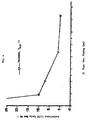
- the measurement results shown graphically in FIG. 4 show one actual memory failure in the PC as the cause with the aid of the activation of the corresponding high-impedance signal development time test mode Bit line contact could be determined.
- the curve representing the measurement results in FIG. 4 clearly shows that from about 0.5 ns above 0.0
- the default value is the failure rate determined in the memory test program is almost zero and also at higher values the Signal Development Time had no failures were.
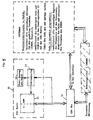
- FIG. 5 summarizes those for activating Test modes in the working memory 8 of a PC during its normal Operating proposed combination of one on one Plug-in card 21 provided circuit arrangement, for example can be plugged into an ISA bus slot 12 (FIG. 1) is, together with special system-related software.
- the circuit arrangement given as an example on the ISA card 21 has the additional memory 22, the z. B. from two 8-bit SRAM chips with a total of 16 bits of data access there is an address and I / O output encoding logic 23 and one Display coding logic 24 on.
- designated blocks are those related to the user interface Programs programmed in the high-level language PASCAL. This program code calculates all necessary addresses for the selected test mode, for SDRAM, chipset, modified the required code and copies it into the additional memory 22, executes the code and jumps back to the calling program. The test mode is therefore called in the high-level language program under MS DOS.
- test mode is programmed in assembler. In this Assembler program will have all the necessary registers of the Chipset and processor modified, the CACHE memory deactivated and the test mode of the SDRAM addressed.
- the invention enables the use of all in SDRAM chips implemented test modes in standard personal computers and with standard operating systems. They also offer Test modes for the first time, by varying different internal parameters, such as B. internal voltages and timings, used in the usual personal computer SDRAM analyze the real cause of an error. With the error analysis, additional optimizations can be made perform on the SDRAM chip and also a determined Variation of internal parameters for a final design of a Use SDRAM chips.
Landscapes
- Tests Of Electronic Circuits (AREA)
- For Increasing The Reliability Of Semiconductor Memories (AREA)
- Techniques For Improving Reliability Of Storages (AREA)
Abstract
Description
- Fig. 1
- in Form eines Blockschaltbilds Funktionsblöcke eines handelsüblichen Personal Computers, in dem sich das erfindungsgemäße Verfahren mit einer zur Durchführung des Verfahrens eingerichteten Vorrichtung durchführen lässt;
- Fig. 2
- ein Ablaufdiagramm zur Erläuterung der für die Aktivierung aller Testmodi wesentlichen Schritte des erfindungsgemäßen Verfahrens;
- Fig. 3
- graphisch Ausfallraten von SDRAM-Modulen, die sich beim ersten Testmodus bei der Veränderung der internen Spannung ergaben;
- Fig. 4
- graphisch Ausfallraten, die sich bei der Durchführung eines zweiten Testmodus, bei dem mittels des erfindungsgemäßen Verfahrens ein internes Timing des SDRAM-Chips verändert wird, einstellten; und
- Fig. 5
- ein Funktionsblockschaltbild mit einer eine zur Durchführung des erfindungsgemäßen Verfahrens eingerichtete Schaltungsanordnung aufweisenden ISA-Steckkarte.
- die Berechnung von 32-Bit-Adressen in Zeilen-, Spalten- und Bankadressen (Adressenmultiplex);
- die Steuerung der SDRAMs mit Steuersignalen CS, RAS, CAS, usw.;
- die Betriebsart des SDRAMs; sowie
- eine Entscheidung, welche Modulbank für einen momentanen Task zu verwenden ist.
Claims (7)
- Verfahren zum Testen eines als Arbeitsspeicher im Personal Computer (PC) eingesetzten SDRAM-Speichers, in dem wenigstens ein vorbestimmter herstellerdefinierter interner Testmodus implementiert ist,
gekennzeichnet durch
folgende Schritte:A) Speichern wenigstens einer zur Aktivierung und Durchführung wenigstens eines der internen Testmodi geeigneten Befehlsfolge im Maschinencode in einem vom Arbeitsspeicher separaten Zusatzspeicher;B) im PC wird der Maschinencode aktiviert und der CACHE-Speicher abgeschaltet;C) die CPU wird in den UNREAL-MODE versetzt, wobei die Datensegmentierung des Arbeitsspeichers aufgehoben wird;D) im PC werden für eine Aktivierungssequenz des Testmodus im SDRAM vorbestimmte Einstellungen des PC-Chipsatzes durchgeführt;E) benutzerdefiniert wird ein gewünschter Testmodus von den im SDRAM-Speicher implementierten Testmodi ausgewählt und daraufhin ein Lese-Zugriff auf den separaten Zusatzspeicher zur Ausführung der Befehlsfolge für die Aktivierung des Testmodus ausgeführt, wobei ;F) der Testmodus durch eine bestimmte Sequenz von Kommandos und Adressen vom Speichercontroller an den SDRAM-Speicher aktiviert wird, die durch die Befehlsfolge im Zusatzspeicher gesteuert wird, undH) Testergebnisse werden protokolliert. - Verfahren nach Anspruch 1,
dadurch gekennzeichnet,
dass in Schritt A) eine Befehlsfolge zur Aktivierung eines ersten chip-internen Testmodus zur Veränderung einer internen Spannung (Vref) des SDRAM-Speicherchips gespeichert und in den Schritten B) bis G) dieser erste Testmodus aktiviert und ausgeführt wird. - Verfahren nach Anspruch 2,
dadurch gekennzeichnet,
dass der erste Testmodus von einem Standardwert der Referenzspannung (Vref) ausgeführt wird. - Verfahren nach Anspruch 1,
dadurch gekennzeichnet,
dass im Schritt A) eine Befehlsfolge zur Aktivierung eines zweiten internen Testmodus zur Veränderung einer chip-internen Zeitdauer ("Signal Development Timing"), die die Zeitdauer zwischen dem Aktivieren der Wortleitung und dem Aktivieren des zugehörigen Sense-Verstärkers angibt, gespeichert und in den Schritten B) bis G) dieser zweite Testmodus aktiviert und ausgeführt wird. - Verfahren nach einem der Ansprüche 1 bis 4,
dadurch gekennzeichnet,
dass das Verfahren folgende weitere Schritte aufweist:H) nach Ausführung des Testmodus in Schritt F) und Protokollierung der Testergebnisse in Schritt G) werden die im Schritt D) vorgenommenen Einstellungen des PC-Chipsatzes rückgängig gemacht;I) die Datensegmentierung des Arbeitsspeichers wird durch Versetzen der CPU in den REAL-MODE wiederhergestellt;K) der CACHE-Speicher wird wieder eingeschaltet, undL) es erfolgt ein Rücksprung ins aufrufende Programm, wobei der SDRAM-Speicher im gewählten Testmodus bleibt, so dass dessen Auswirkung dem SDRAM-Speicher erhalten bleibt. - Vorrichtung zur Durchführung des Verfahrens nach einem der Ansprüche 1 bis 5,
dadurch gekennzeichnet,
dass der Zusatzspeicher (22) auf einer steckbaren Schaltungsplatte (21) vorgesehen ist. - Vorrichtung nach Anspruch 6,
dadurch gekennzeichnet,
dass die Schaltungsplatte (21) eine 16-Bit-ISA-Karte ist und als Zusatzspeicher zwei 8-Bit-SRAM-Bausteine mit einem insgesamt 16 Bit breiten Datenzugriff aufweist.
Applications Claiming Priority (2)
| Application Number | Priority Date | Filing Date | Title |
|---|---|---|---|
| DE10007177 | 2000-02-17 | ||
| DE10007177A DE10007177C2 (de) | 2000-02-17 | 2000-02-17 | Verfahren zum Testen eines als Arbeitsspeicher im Personal Computer eingesetzten SDRAM-Speichers |
Publications (2)
| Publication Number | Publication Date |
|---|---|
| EP1126475A2 true EP1126475A2 (de) | 2001-08-22 |
| EP1126475A3 EP1126475A3 (de) | 2006-03-08 |
Family
ID=7631260
Family Applications (1)
| Application Number | Title | Priority Date | Filing Date |
|---|---|---|---|
| EP01103000A Withdrawn EP1126475A3 (de) | 2000-02-17 | 2001-02-08 | Verfahren und Vorrichtung zum Testen eines als Arbeitsspeicher im Personal Computer eingesetzten SDRAM-Speichers |
Country Status (4)
| Country | Link |
|---|---|
| US (1) | US6775795B2 (de) |
| EP (1) | EP1126475A3 (de) |
| DE (1) | DE10007177C2 (de) |
| TW (1) | TW559819B (de) |
Families Citing this family (6)
| Publication number | Priority date | Publication date | Assignee | Title |
|---|---|---|---|---|
| DE10213009A1 (de) | 2002-03-22 | 2003-10-09 | Infineon Technologies Ag | Verfahren zum elektronischen Testen von Speichermodulen |
| DE10330037B3 (de) | 2003-07-03 | 2005-01-20 | Infineon Technologies Ag | Adapterkarte zum Anschließen an einen Datenbus in einer Datenverarbeitungseinheit und Verfahren zum Betreiben eines DDR-Speichermoduls |
| DE10335132B3 (de) * | 2003-07-31 | 2004-12-09 | Infineon Technologies Ag | Speicheranordnung eines Computersystems |
| DE10344877B3 (de) * | 2003-09-26 | 2004-12-30 | Infineon Technologies Ag | Vorrichtung zum Testen eines Speichermoduls |
| US20050289287A1 (en) * | 2004-06-11 | 2005-12-29 | Seung-Man Shin | Method and apparatus for interfacing between test system and embedded memory on test mode setting operation |
| DE102006045906A1 (de) * | 2006-09-28 | 2008-04-17 | Infineon Technologies Ag | Modul mit einem Controller für eine Chipkarte |
Family Cites Families (9)
| Publication number | Priority date | Publication date | Assignee | Title |
|---|---|---|---|---|
| US4528636A (en) * | 1981-10-19 | 1985-07-09 | Intermark Industries, Inc. | Display memory with write inhibit signal for transparent foreground pixel codes |
| JPH0969300A (ja) * | 1995-06-23 | 1997-03-11 | Mitsubishi Electric Corp | 半導体記憶装置 |
| US5862320A (en) * | 1995-12-22 | 1999-01-19 | Cirrus Logic, Inc. | SDRAM DIMM presence detect interface |
| US5995424A (en) * | 1997-07-16 | 1999-11-30 | Tanisys Technology, Inc. | Synchronous memory test system |
| US6112276A (en) * | 1997-10-10 | 2000-08-29 | Signatec, Inc. | Modular disk memory apparatus with high transfer rate |
| US5889714A (en) * | 1997-11-03 | 1999-03-30 | Digital Equipment Corporation | Adaptive precharge management for synchronous DRAM |
| US6119252A (en) * | 1998-02-10 | 2000-09-12 | Micron Technology | Integrated circuit test mode with externally forced reference voltage |
| JP2000021193A (ja) * | 1998-07-01 | 2000-01-21 | Fujitsu Ltd | メモリ試験方法及び装置並びに記憶媒体 |
| US5999468A (en) * | 1998-11-17 | 1999-12-07 | Tanisys Technology, Inc. | Method and system for identifying a memory module configuration |
-
2000
- 2000-02-17 DE DE10007177A patent/DE10007177C2/de not_active Expired - Fee Related
-
2001
- 2001-02-08 EP EP01103000A patent/EP1126475A3/de not_active Withdrawn
- 2001-02-20 US US09/789,991 patent/US6775795B2/en not_active Expired - Fee Related
- 2001-03-09 TW TW090103371A patent/TW559819B/zh not_active IP Right Cessation
Also Published As
| Publication number | Publication date |
|---|---|
| US20010025354A1 (en) | 2001-09-27 |
| DE10007177C2 (de) | 2002-03-14 |
| TW559819B (en) | 2003-11-01 |
| EP1126475A3 (de) | 2006-03-08 |
| DE10007177A1 (de) | 2001-09-06 |
| US6775795B2 (en) | 2004-08-10 |
Similar Documents
| Publication | Publication Date | Title |
|---|---|---|
| DE102004021267B4 (de) | Verfahren zum Testen eines Speicherbausteins und Prüfanordnung | |
| DE3412676C2 (de) | ||
| DE102006038033A1 (de) | Speicherarray-Architektur und Verfahren zum schnellen Messen von einer Verteilung | |
| EP2100308B1 (de) | Verfahren und halbleiterspeicher mit einer einrichtung zur erkennung von adressierungsfehlern | |
| EP0104635A2 (de) | Verfahren und Anordnung zum Prüfen eines digitalen Rechners | |
| DE19963689A1 (de) | Schaltungsanordnung eines integrierten Halbleiterspeichers zum Speichern von Adressen fehlerhafter Speicherzellen | |
| DE10007177C2 (de) | Verfahren zum Testen eines als Arbeitsspeicher im Personal Computer eingesetzten SDRAM-Speichers | |
| DE19721516C2 (de) | Mikroprozessor | |
| DE2549392B2 (de) | Verfahren zur erhoehung der zuverlaessigkeit von integrierten speicherbausteinen und zur verbesserung der ausbeute von nach aussen hin fehlerfrei erscheinenden speicherbausteinen bei ihrer herstellung | |
| DE3916811C2 (de) | ||
| DE10323237B4 (de) | Verfahren und Vorrichtung zur Optimierung der Funktionsweise von DRAM-Speicherelementen | |
| DE60128596T2 (de) | Interrupt-steuerung für einen mikroprozessor | |
| DE102006019426B4 (de) | Speichermodulsteuerung, Speichersteuerung und entsprechende Speicheranordnung sowie Verfahren zur Fehlerkorrektur | |
| DE102004040507A1 (de) | Referenzspannungsdetektor für eine Leistungseinschaltsequenz in einem Speicher | |
| DE102005060901A1 (de) | Verfahren zur Erkennung einer Versorgungsunterbrechung in einem Datenspeicher und zur Wiederherstellung des Datenspeichers | |
| DE102016104336A1 (de) | Verfahren zur Überwachung des Betriebs einer Speichervorrichtung vom Typ EEPROM und entsprechende Vorrichtung | |
| DE102017115056B3 (de) | Verfahren zur Überprüfung sicherheitsrelevanter Register- oder Speicherzellen auf Stuck-At-Fehler im Betrieb | |
| DE102017115058B4 (de) | Verfahren zur Überprüfung sicherheitsrelevanter Register- oder Speicherzellen auf Stuck-At-Fehler im Betrieb und Herbeiführung der Ausfallsicherheit | |
| EP1594063B1 (de) | Verfahren zum Überprüfen von Steuerungsprogrammen | |
| DE102017115057B4 (de) | Verfahren zur Überprüfung sicherheitsrelevanter Register- oder Speicherzellen auf Stuck-At-Fehler im Betrieb durch Vergleich zweier Schreibvorgänge mit unterschiedlichem Inversionsstatus | |
| DE10311428A1 (de) | Vorrichtung zur Erkennung und/oder Korrektur von Fehlern in aus einer Speichereinrichtung ausgelesenen Daten | |
| DE102006049205A1 (de) | Chipspezifische Ausführung eines Testmodus an einem Speichermodul | |
| DE3817857C2 (de) | ||
| DE102014203963A1 (de) | Verfahren und Vorrichtung zum Kontrollieren eines Speichers | |
| DE102004051158A1 (de) | Integrierter Halbleiterspeicher |
Legal Events
| Date | Code | Title | Description |
|---|---|---|---|
| PUAI | Public reference made under article 153(3) epc to a published international application that has entered the european phase |
Free format text: ORIGINAL CODE: 0009012 |
|
| AK | Designated contracting states |
Kind code of ref document: A2 Designated state(s): AT BE CH CY DE DK ES FI FR GB GR IE IT LI LU MC NL PT SE TR |
|
| AX | Request for extension of the european patent |
Free format text: AL;LT;LV;MK;RO;SI |
|
| PUAL | Search report despatched |
Free format text: ORIGINAL CODE: 0009013 |
|
| AK | Designated contracting states |
Kind code of ref document: A3 Designated state(s): AT BE CH CY DE DK ES FI FR GB GR IE IT LI LU MC NL PT SE TR |
|
| AX | Request for extension of the european patent |
Extension state: AL LT LV MK RO SI |
|
| 17P | Request for examination filed |
Effective date: 20060809 |
|
| 17Q | First examination report despatched |
Effective date: 20061006 |
|
| AKX | Designation fees paid |
Designated state(s): DE GB IE |
|
| STAA | Information on the status of an ep patent application or granted ep patent |
Free format text: STATUS: THE APPLICATION IS DEEMED TO BE WITHDRAWN |
|
| 18D | Application deemed to be withdrawn |
Effective date: 20070217 |