EP1122796B1 - Vertikales Halbleiterbauelement mit Source-Down-Design und entsprechendes Herstellungsverfahren - Google Patents
Vertikales Halbleiterbauelement mit Source-Down-Design und entsprechendes Herstellungsverfahren Download PDFInfo
- Publication number
- EP1122796B1 EP1122796B1 EP01102123A EP01102123A EP1122796B1 EP 1122796 B1 EP1122796 B1 EP 1122796B1 EP 01102123 A EP01102123 A EP 01102123A EP 01102123 A EP01102123 A EP 01102123A EP 1122796 B1 EP1122796 B1 EP 1122796B1
- Authority
- EP
- European Patent Office
- Prior art keywords
- layer
- trench
- region
- conduction type
- substrate
- Prior art date
- Legal status (The legal status is an assumption and is not a legal conclusion. Google has not performed a legal analysis and makes no representation as to the accuracy of the status listed.)
- Expired - Lifetime
Links
- 239000004065 semiconductor Substances 0.000 title claims description 31
- 238000000034 method Methods 0.000 title claims description 12
- 238000004519 manufacturing process Methods 0.000 title description 7
- 239000000758 substrate Substances 0.000 claims description 26
- 238000002513 implantation Methods 0.000 claims description 10
- 210000000746 body region Anatomy 0.000 claims description 9
- 229910021332 silicide Inorganic materials 0.000 claims description 8
- FVBUAEGBCNSCDD-UHFFFAOYSA-N silicide(4-) Chemical compound [Si-4] FVBUAEGBCNSCDD-UHFFFAOYSA-N 0.000 claims description 8
- 238000000151 deposition Methods 0.000 claims description 6
- 229910052751 metal Inorganic materials 0.000 claims description 5
- 239000002184 metal Substances 0.000 claims description 5
- WFKWXMTUELFFGS-UHFFFAOYSA-N tungsten Chemical compound [W] WFKWXMTUELFFGS-UHFFFAOYSA-N 0.000 claims description 3
- 229910052721 tungsten Inorganic materials 0.000 claims description 3
- 239000010937 tungsten Substances 0.000 claims description 3
- 238000002955 isolation Methods 0.000 description 8
- 238000005530 etching Methods 0.000 description 6
- 230000008021 deposition Effects 0.000 description 4
- 229910021420 polycrystalline silicon Inorganic materials 0.000 description 4
- 229920005591 polysilicon Polymers 0.000 description 4
- XUIMIQQOPSSXEZ-UHFFFAOYSA-N Silicon Chemical compound [Si] XUIMIQQOPSSXEZ-UHFFFAOYSA-N 0.000 description 2
- 238000009413 insulation Methods 0.000 description 2
- 229910052710 silicon Inorganic materials 0.000 description 2
- 239000010703 silicon Substances 0.000 description 2
- 230000015572 biosynthetic process Effects 0.000 description 1
- 239000005380 borophosphosilicate glass Substances 0.000 description 1
- 238000010586 diagram Methods 0.000 description 1
- 238000009792 diffusion process Methods 0.000 description 1
- 230000005669 field effect Effects 0.000 description 1
- 230000003071 parasitic effect Effects 0.000 description 1
- 239000005368 silicate glass Substances 0.000 description 1
Images


Classifications
-
- H—ELECTRICITY
- H01—ELECTRIC ELEMENTS
- H01L—SEMICONDUCTOR DEVICES NOT COVERED BY CLASS H10
- H01L29/00—Semiconductor devices adapted for rectifying, amplifying, oscillating or switching, or capacitors or resistors with at least one potential-jump barrier or surface barrier, e.g. PN junction depletion layer or carrier concentration layer; Details of semiconductor bodies or of electrodes thereof ; Multistep manufacturing processes therefor
- H01L29/66—Types of semiconductor device ; Multistep manufacturing processes therefor
- H01L29/68—Types of semiconductor device ; Multistep manufacturing processes therefor controllable by only the electric current supplied, or only the electric potential applied, to an electrode which does not carry the current to be rectified, amplified or switched
- H01L29/76—Unipolar devices, e.g. field effect transistors
- H01L29/772—Field effect transistors
- H01L29/78—Field effect transistors with field effect produced by an insulated gate
- H01L29/7801—DMOS transistors, i.e. MISFETs with a channel accommodating body or base region adjoining a drain drift region
- H01L29/7802—Vertical DMOS transistors, i.e. VDMOS transistors
- H01L29/7813—Vertical DMOS transistors, i.e. VDMOS transistors with trench gate electrode, e.g. UMOS transistors
-
- H—ELECTRICITY
- H01—ELECTRIC ELEMENTS
- H01L—SEMICONDUCTOR DEVICES NOT COVERED BY CLASS H10
- H01L29/00—Semiconductor devices adapted for rectifying, amplifying, oscillating or switching, or capacitors or resistors with at least one potential-jump barrier or surface barrier, e.g. PN junction depletion layer or carrier concentration layer; Details of semiconductor bodies or of electrodes thereof ; Multistep manufacturing processes therefor
- H01L29/66—Types of semiconductor device ; Multistep manufacturing processes therefor
- H01L29/68—Types of semiconductor device ; Multistep manufacturing processes therefor controllable by only the electric current supplied, or only the electric potential applied, to an electrode which does not carry the current to be rectified, amplified or switched
- H01L29/76—Unipolar devices, e.g. field effect transistors
- H01L29/772—Field effect transistors
- H01L29/78—Field effect transistors with field effect produced by an insulated gate
- H01L29/7801—DMOS transistors, i.e. MISFETs with a channel accommodating body or base region adjoining a drain drift region
- H01L29/7802—Vertical DMOS transistors, i.e. VDMOS transistors
- H01L29/781—Inverted VDMOS transistors, i.e. Source-Down VDMOS transistors
-
- H—ELECTRICITY
- H01—ELECTRIC ELEMENTS
- H01L—SEMICONDUCTOR DEVICES NOT COVERED BY CLASS H10
- H01L29/00—Semiconductor devices adapted for rectifying, amplifying, oscillating or switching, or capacitors or resistors with at least one potential-jump barrier or surface barrier, e.g. PN junction depletion layer or carrier concentration layer; Details of semiconductor bodies or of electrodes thereof ; Multistep manufacturing processes therefor
- H01L29/40—Electrodes ; Multistep manufacturing processes therefor
- H01L29/41—Electrodes ; Multistep manufacturing processes therefor characterised by their shape, relative sizes or dispositions
- H01L29/423—Electrodes ; Multistep manufacturing processes therefor characterised by their shape, relative sizes or dispositions not carrying the current to be rectified, amplified or switched
- H01L29/42312—Gate electrodes for field effect devices
- H01L29/42316—Gate electrodes for field effect devices for field-effect transistors
- H01L29/4232—Gate electrodes for field effect devices for field-effect transistors with insulated gate
- H01L29/42364—Gate electrodes for field effect devices for field-effect transistors with insulated gate characterised by the insulating layer, e.g. thickness or uniformity
- H01L29/42368—Gate electrodes for field effect devices for field-effect transistors with insulated gate characterised by the insulating layer, e.g. thickness or uniformity the thickness being non-uniform
Definitions
- the present invention relates to a vertical semiconductor device with source-down design and a corresponding manufacturing method.
- DE 196 38 439 A1 discloses a field effect controllable vertical semiconductor device comprising a semiconductor body having at least one drain region of the first conductivity type, at least one source region of the first conductivity type, at least one body region of the second conductivity type between the drain and source regions and at least one gate electrode, which is insulated from the entire semiconductor body by a gate oxide, the gate terminal and drain terminal being on the disc front side and the source terminal being on the Scheieben reverse side.
- EP-A-0 440 394 discloses a vertical MOSFET transistor comprising a semiconductor substrate having a first and a second surface, a drain region at the first surface, a channel forming region below the drain region, a source region below the channel forming region, a gate dielectric having one A gate electrode formed on a portion of the channel forming region between the source and the drain to affect the conductivity therebetween, and a buried ohmic contact shorting a part of the channel forming region to the underlying source region.
- WO-A-99/36964 discloses a FET having a source-substrate terminal and a buried gate, wherein a drain region of a first conductivity type is provided on a surface of a semiconductor layer of the first conductivity type disposed on a semiconductor substrate of the first conductivity type, a trench gate substantially Semiconductor layer interspersed, at the end of the trench on the other surface of the semiconductor layer, a source region of the first conductivity type is provided in the region next to the trench on the other surface of the semiconductor layer, a semiconductor zone of a second conductivity type is provided, whose surface together with the surface of the source region the other Surface of the semiconductor layer is formed, and a buried high-conductivity layer between the other surface of the semiconductor layer and the semiconductor substrate is provided.
- Source-down power transistors offer both circuit-breaker and integrated circuit breaker (with common source) advantages of circuit and thermal nature.
- a problem in their manufacture is that the source region and the body region, which are buried in the silicon, must be short-circuited so that the parasitic biopolar transistor does not turn on.
- this object is achieved by the semiconductor device specified in claim 1 or by the manufacturing method specified in claim 7.
- the short circuit between body region and source region is realized in the lower region of the trench, wherein not the substrate but an additional, preferably implanted region serves as the source region, which is short-circuited with the substrate and the body region, for example via a silicide.
- An advantage of the embodiment according to the invention is that the short circuit between body region and source region is realized in a space-saving manner in the lower region of the trench.
- At least one of the first, second and third layer is an epitaxial layer.
- the source region is an implantation region.
- the conductive layer is a silicide layer.
- the silicide layer is created by depositing a metal, preferably tungsten, in the trench and thermal siliciding.
- the first conductivity type is the n-conductivity type.
- the second layer is formed by an implantation in the trench bottom and an outdiffusion before the source implantation.
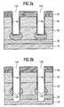
- Fig. 1 is a schematic diagram of a semiconductor device embodying the present invention.
- 10 designates an n + substrate, 20 a p + epitaxial layer (body lead), 30 a p epitaxial layer (body), 40 an n epitaxial layer (drain), 50 a drain, 60 an isolation region, 70 a Drain contact, 80 a first isolation layer, 90 a gate, 100 a gate oxide, 110 a second isolation layer, 120 a silicide region, 130 a source region and 140 a trench.
- This embodiment is a power-down power transistor having a n + -line type substrate.
- a first, second and third Epitaxiechicht 20, 30, 40 substrate 10 are provided on the n +, namely the first layer 20 of the p + conduction type on the substrate 10 as body connection region, the second layer 30 of p-conductivity type first on the Layer 20 as a body region and the third layer 40 of the n-type conductivity n on the second layer 30 as a drain region.
- the trench 140 which extends down to the substrate 10, includes a gate structure 90, 100 having a gate 90 and a gate oxide 100, the gate 100 being isolated from its surroundings by the isolation layers 90 and 110 and the isolation region 60.
- the source region 130 of the n + -line type is an implantation region.
- the source region 130 is characterized by a conductive layer 120 provided in the lower trench region in the form of a silicide layer is short-circuited with the first layer 20 and the substrate 10.
- Fig. 1 two such transistors are shown, wherein the right-hand transistor has a gate 90 connected to the right or connected to the outside and the left transistor has a gate 90 connected or interconnected to the rear (third dimension) by a transverse trench (not shown) ,
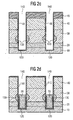
- FIGS. 2 a - f are schematic illustrations of the essential method steps for producing the semiconductor component according to FIG. 1.
- the n.sup. + Substrate 10 is provided and then the first p + type first layer 20 is epitaxially formed on the substrate 10, the second conductivity type second layer 30 on the first layer 20, and the third conductivity type third layer 40 n on the second layer 30.
- An oxide 45 is deposited thereon and a trench 140, which extends down to the second layer 20, is formed. The latter is done by forming a photomask on the oxide 45 and an anisotropic etching of the oxide 45 (hardmask) and the trench. Subsequently, a stray oxide 48 is formed in the trench 140. Thereafter, the implantation and diffusion of the source region 130 of the conduction type n + is performed in the lower part of the second layer 30 in the periphery of the trench 140.
- the trench 140 is then deepened down to the substrate 10, as illustrated in FIG. 2b.
- shorting of the source region 130 is accomplished by forming the conductive layer 120 in the lower trench region with the first layer 20 and the substrate 10.
- a metal e.g. Tungsten
- Subsequent etching removes the residual oxide metal.
- the deposition of oxide 110, the application of an auxiliary layer 55 and the etching back of the auxiliary layer 55 are then carried out.
- the oxide 110 is etched in the region above the remaining auxiliary layer 55 and a gate oxide 100 is formed. Then, the auxiliary layer 55 is removed and gate polysilicon is deposited over the resulting structure. The gate polysilicon is optionally doped and then etched back.
- a thicker oxide 80 is formed analogously to the oxide 110 in the upper region of the trench thermally or by deposition.
- anisotropic etching of the oxide 80 is then carried out in order to remove it from the top side of the gate polysilicon 90 and then a new deposition, doping and etching back of further gate polysilicon 90.
- Silicate glass (BPSG) is finally the isolation region 60 formed on the top of the trench.
- Contact holes for the drain connection are formed by means of a mask and the drain contact 70 is self-aligning implanted. Finally, the formation of the metal level takes place for the drain 50 to complete the transistor.
- the body is not realized by an epitaxial layer but by a p-implantation in the trench bottom and an outdiffusion before the source implantation.
- the present invention is not limited to the described transistor but may be applied to any more complicated structure, e.g. a thyristor structure can be applied.
- the body connection area is not absolutely necessary, but it is also possible to connect the body area directly.
Description
- Die vorliegende Erfindung betrifft ein vertikales Halbleiterbauelement mit Source-Down-Design sowie ein entsprechendes Herstellungsverfahren.
- Die DE 196 38 439 A1 offenbart ein durch Feldeffekt steuerbares, vertikales Halbleiterbauelement, bestehend aus einem Halbleiterkörper mit mindestens einem Draingebiet vom ersten Leitungstyp, mindestens einem Sourcegebiet vom ersten Leitungstyp, mindestens einem Bodygebiet vom zweiten Leitungstyp zwischen Drain- und Sourcegebiet und mindestens einer Gateelektrode, die gegenüber dem gesamten Halbleiterkörper durch ein Gateoxid isoliert ist, wobei sich der Gateanschluß und Drainanschluß auf der Scheibenvorderseite und der Sourceanschluß auf der Scheiebenrückseite befindet.
- Die EP-A-0 440 394 offenbart einen vertikalen MOSFET-Transistor mit einem Halbleitersubstrat mit einer ersten und einer zweiten Oberfläche, einem Drainbereich an der ersten Oberfläche, einem kanalbildenden Bereich unter dem Drainbereich, einem Sourcebereich unter dem kanalbildenden Bereich, einem Gatedielektrikum mit einer Gateelektrode, die auf einem Teilbereich des kanalbildenden Bereichs zwischen Source und Drain ausgebildet sind um die Leitfähigkeit dazwischen zu beeinflussen, und einem vergrabenen ohmschen Kontakt, der einen Teil des kanalbildenden Bereichs mit dem darunter liegenden Sourcebereich kurzschließt.
- Die WO-A-99/36964 offenbart einen FET mit Source-Substratanschluss und vergrabenem Gate, wobei eine Drainzone eines ersten Leitungstyps an einer Oberfläche einer auf einem Halbleitersubstrat des ersten Leitungstyps angeordneten Halbleiterschicht des ersten Leitungstyps vorgesehen ist, ein Graben-Gate im wesentlichen die Halbleiterschicht durchsetzt, am Ende des Grabens an der anderen Oberfläche der Halbleiterschicht eine Sourcezone des ersten Leitungstyps vorgesehen ist, im Gebiet neben dem Graben an der anderen Oberfläche der Halbleiterschicht eine Halbleiterzone eines zweiten Leitungstyps vorgesehen ist, deren Oberfläche zusammen mit der Oberfläche der Sourcezone die andere Oberfläche der Halbleiterschicht bildet, und eine vergrabene hochleitende Schicht zwischen der anderen Oberfläche der Halbleiterschicht und dem Halbleitersubstrat vorgesehen ist.
- Obwohl auf beliebige Halbleiterbauelemente anwendbar, werden die vorliegende Erfindung sowie die ihr zu Grunde liegende Problematik in Bezug auf vertikale Source-Down-Leistungstransistoren erläutert.
- Source-Down-Leistungstransistoren bieten als Einzelschalter sowie als integrierte Merhfachschalter (mit Common Source = gemeinsamer Sourceanschluss) Vorteile schaltungstechnischer und thermischer Art.
- Ein Problem bei ihrer Herstellung besteht darin, dass das Sourcegebiet und das Bodygebiet, welche im Silizium vergraben sind, kurzgeschlossen sein müssen, damit der parasitäre Biopolartransistor nicht einschaltet.
- Daher ist es Aufgabe der vorliegenden Erfindung, ein Halbleiterbauelement der eingangs genannten Art bereitzustellen, bei dem der Kurzschluß zwischen Sourcegebiet und Bodygebiet prozeßtechnisch günstig herstellbar ist. Eine weitere Aufgabe besteht in der Bereitstellung eines entsprechenden Herstellungsverfahrens.
- Erfindungsgemäß wird diese Aufgabe durch das in Anspruch 1 angegebene Halbleiterbauelement bzw. durch das in Anspruch 7 angegebene Herstellungsverfahren gelöst.
- Die der vorliegenden Erfindung zugrundeliegende Idee besteht darin, daß das Halbleiterbauelement als Trenchbauelement (Trench = Graben) realisiert wird, wobei der Trench die Gateelektrode enthält. Der Kurzschluß zwischen Bodygebiet und Sourcegebiet ist im unteren Bereich des Trenchs realisiert, wobei nicht das Substrat, sondern ein zusätzlicher, vorzugsweise implantierter Bereich als Sourcebereich dient, welcher mit dem Substrat und dem Bodybereich beispielsweise über ein Silizid kurzgeschlossen ist.
- Dabei ist es zweckmäßig, eine Prozeßfolge vorzusehen, die eine Isolation des Gates vom Kurzschluß zwischen Bodygebiet und Sourcegebiet sowie eine dickere Isolation im oberen Teil des Trenches zur Isolation zwischen Drain und Gate schafft.
- Ein Vorteil der erfindungsgemäßen Ausgestaltung besteht darin, daß der Kurzschluß zwischen Bodygebiet und Sourcegebiet platzsparend im unteren Bereich des Trenchs realisiert ist.
- In den Unteransprüchen finden sich vorteilhafte Weiterbildungen und Verbesserungen des in Anspruch 1 angegebenen Halbleiterbauelements bzw. des in Anspruch 7 angegebenen Herstellungsverfahrens.
- Gemäß einer bevorzugten Weiterbildung ist mindestens eine der ersten, zweiten und dritten Schicht eine Epitaxieschicht.
- Gemäß einer weiteren bevorzugten Weiterbildung ist der Sourcebereich ein Implantationsbereich.
- Gemäß einer weiteren bevorzugten Weiterbildung ist die leitende Schicht eine Silizidschicht.
- Gemäß einer weiteren bevorzugten Weiterbildung wird die Silizidschicht durch Abscheiden von einem Metall, vorzugsweise Wolfram, in dem Graben und thermisches Silizidieren geschaffen.
- Gemäß einer weiteren bevorzugten Weiterbildung ist der erste Leitungstyp der n-Leitungstyp.
- Gemäß einer weiteren bevorzugten Weiterbildung wird die zweite Schicht durch eine Implantation in den Trenchboden und eine Ausdiffusion vor der Sourceimplantation gebildet.
- Ausführungsbeispiele der Erfindung sind in den Zeichnungen dargestellt und in der nachfolgenden Beschreibung näher erläutert.
- Es zeigen:
- Fig. 1
- eine schematische Darstellung eines Halbleiterbauelements als Ausführungsform der vorliegenden Erfindung; und
- Fig. 2a-e
- eine schematische Darstellung der wesentlichen Verfahrensschritte zur Herstellung des Halbleiterbauelements nach Fig. 1.
- In den Figuren bezeichnen gleiche Bezugszeichen gleiche oder funktionsgleiche Elemente.
- Fig. 1 ist eine schematische Darstellung eines Halbleiterbauelements als Ausführungsform der vorliegenden Erfindung.
- In Fig. 1 bezeichnen 10 ein n+-Substrat, 20 eine p+-Epitaxieschicht (Bodyanschluß), 30 eine p-Epitaxieschicht (Body), 40 eine n-Epitaxieschicht (Drain), 50 einen Drainanschluß, 60 einen Isolationsbereich, 70 einen Drainkontakt, 80 eine erste Isolationsschicht, 90 ein Gate, 100 ein Gateoxid, 110 eine zweite Isolationsschicht, 120 einen Silizidbereich, 130 einen Sourcebereich und 140 einen Graben.
- Bei dieser Ausführungsform handelt es sich um einen Soürce-Down-Leistungstransistor mit einem Substrat des n+-Leitungstyps.
- Eine erste, zweite und dritte Epitaxiechicht 20, 30, 40 sind auf dem n+-Substrat 10 vorgesehen, nämlich die erste Schicht 20 des p+-Leitungstyps auf dem Substrat 10 als Bodyanschlußbereich, die zweite Schicht 30 des p-Leitungstyps auf der ersten Schicht 20 als Bodybereich und die dritte Schicht 40 des n-Leitungstyps n auf der zweiten Schicht 30 als Drainbereich.
- Der Graben 140, welcher bis zum Substrat 10 hinunter reicht, enthält eine Gatestruktur 90, 100 mit einem Gate 90 und einem Gateoxid 100, wobei das Gate 100 durch die Isolationsschichten 90 und 110 sowie den Isolationsbereich 60 von seiner Umgebung isoliert ist.
- In der zweiten Schicht 30 in der Peripherie des Grabens 140 vorgesehen ist der Sourcebereich 130 des n+-Leitungstyps, der ein Implantationsbereich ist. Der Sourcebereich 130 ist durch eine im unteren Grabenbereich vorgesehene leitende Schicht 120 in Form einer Silizidschicht mit der ersten Schicht 20 und dem Substrat 10 kurzgeschlossen.
- In Fig. 1 sind zwei solche Transistoren gezeigt, wobei der rechte Transistor ein nach rechts außen hin angeschlossenes bzw. verschaltetes Gate 90 aufweist und der linke Transistor ein durch einen nicht dargestellten Quertrench nach hinten (dritte Dimension) hin angeschlossenes bzw. verschaltetes Gate 90 aufweist.
- Fig. 2a-f sind schematische Darstellungen der wesentlichen Verfahrensschritte zur Herstellung des Halbleiterbauelements nach Fig. 1.
- Gemäß Fig. 2a erfolgt ein Bereitstellen des n+-Substrats 10 und danach ein epitaktisches Bilden der ersten Schicht 20 des Leitungstyps p+ auf dem Substrat 10, der zweiten Schicht 30 des Leitungstyps p auf der ersten Schicht 20 und der dritten Schicht 40 des Leitungstyps n auf der zweiten Schicht 30.
- Darauf wird ein Oxid 45 abgeschieden und ein Graben 140, welcher bis zur zweiten Schicht 20 hinunter reicht, gebildet. Letzteres erfolgt durch Bilden einer Photomaske auf dem Oxid 45 und eine anisotrope Ätzung des Oxids 45 (Hartmaske) und des Trenchs. Anschließend wird im Graben 140 ein Streuoxid 48 gebildet. Danach erfolgt das Implantieren und Diffundieren des Sourcebereichs 130 des Leitungstyps n+ im unteren Teil der zweiten Schicht 30 in der Peripherie des Grabens 140.
- Durch eine weitere anisotrope Ätzung erfolgt dann ein Vertiefen des Grabens 140 bis hinunter zum Substrat 10, wie in Fig. 2b illustriert.
- Als nächstes erfolgt gemäß Fig. 2c ein Kurzschließen des Sourcebereichs 130 durch Ausbilden der leitenden Schicht 120 im unteren Grabenbereich mit der ersten Schicht 20 und dem Substrat 10. Hierzu wird ein Metall, z.B. Wolfram, durch eine konforme Abscheidung im Graben gebildet und im unteren Bereich, wo es auf dem Silizium liegt (also unterhalb des verbleibenden Streuoxids 48) durch eine thermische Reaktion in die leitende Schicht 120 aus Silizid umgewandelt. Durch eine anschließende Ätzung wird das restliche, auf Oxid befindliche Metall entfernt.
- Gemäß Fig. 2d erfolgt dann das Abscheiden von Oxid 110, das Aufbringen von einer Hilfsschicht 55 und das Rückätzen der Hilfsschicht 55.
- Wie in Fig. 2e gezeigt, wird das Oxid 110 im Bereich oberhalb der verbleibenden Hilfsschicht 55 geätzt und ein Gate- oxid 100 gebildet. Dann wird die Hilfsschicht 55 entfernt und Gate-Polysilizium über der resultierenden Struktur abgeschieden. Das Gate-Polysilizium wird ggfs. dotiert und dann zurückgeätzt.
- Dann wird, falls zur Isolation notwendig, ein dickeres Oxid 80 analog zum Oxid 110 im oberen Bereich des Grabens thermisch oder durch Abscheidung gebildet.
- Um zur Struktur von Fig. 1 zu gelangen erfolgen danach eine anisotrope Ätzung des Oxids 80, um es von der Oberseite des Gate-Polysiliziums 90 zu entfernen und anschließend eine erneute Abscheidung, Dotierung und Rückätzung weiteren Gate-Polysiliziums 90. Mittels Bor-Phosphor-Silikatglas (BPSG) wird schließlich der Isolationsbereich 60 an der Trenchoberseite gebildet. Mittels einer Maske werden Kontaktlöcher für den Drainanschluß gebildet und der Drainkontakt 70 selbstjustierend implantiert. Schließlich erfolgt die Bildung der Metallebene für den Drainanschluß 50 zur Vervollständigung des Transistors.
- Obwohl die vorliegende Erfindung vorstehend anhand bevorzugter Ausführungsbeispiele beschrieben wurde, ist sie darauf nicht beschränkt, sondern auf vielfältige Art und Weise modifizierbar im Rahmen des beanspruchten Gegenstandes.
- Insbesondere wird in einer weiteren bevorzugten Ausführungsform der Body nicht durch eine Epitaxieschicht realisiert, sondern durch eine p-Implantation in den Trenchboden und eine Ausdiffusion vor der Sourceimplantation.
- Auch ist die vorliegende Erfindung nicht auf dem geschilderten Transistor beschränkt, sondern kann auf eine beliebige kompliziertere Struktur, z.B. eine Thyristorstruktur angewendet werden.
- Weiterhin ist der Bodyanschlußbereich nicht zwingend erforderlich, sondern es ist auch möglich, den Bodybereich direkt anzuschließen.
Claims (13)
- Halbleiterbauelement mit:einem Substrat (10) eines ersten Leitungstyps (n+);einer oberhalb des Substrats (10) vorgesehenen zweiten Schicht (30) des Leitungstyps (p) als Bodybereich;einer auf der zweiten Schicht (30) vorgesehenen dritten Schicht(40) des ersten Leitungstyps (n) als Drainbereich; einem Graben (140), welcher bis zum Substrat (10) hinunter reicht;einer in dem Graben (140) vorgesehenen Gatestruktur (90, 100); undeinem in der zweiten Schicht (30) in der Peripherie des Grabens (140) vorgesehenen Sourcebereich (130) des ersten Leitungstyps (n+);wobei der Sourcebereich (130) durch eine im unteren Grabenbereich vorgesehene leitende Schicht (120) mit der zweiten Schiht (30) und dem Substrat (10) kurzgeschlossen ist.
- Halbleiterbauelement nach Anspruch 1,
dadurch gekennzeichnet,
dass auf dem Substrat (10) eine erste Schicht (20) des zweiten Leitungstyps (p+) als Bodyanschlussbereich vorgesehen ist, auf welcher die zweite Schicht vorgesehen ist. - Halbleiterbauelement nach Anspruch 2,
dadurch gekennzeichnet,
dass mindestens eine der ersten, zweiten und dritten Schicht (20, 30, 40) eine Epitaxieschicht ist. - Halbleiterbauelement nach einem der vorhergehenden Ansprüche,
dadurch gekennzeichnet,
dass der Sourcebereich (130) ein Implantationsbereich ist. - Halbleiterbauelement nach einem der vorhergehenden Ansprüche,
dadurch gekennzeichnet,
dass die leitende Schicht (120) eine Silizidschicht ist. - Halbleiterbauelement nach einem der vorhergehenden Ansprüche,
dadurch gekennzeichnet,
dass der erste Leitungstyp der n-Leitungstyp ist. - Verfahren zur Herstellung eines Halbleiterbauelements mit den Schritten:Bereitstellen von einem Substrat (10) eines ersten Leitungstyps (n+);Vorsehen einer zweiten Schicht (30) des zweiten Leitungstyps (p) oberhalb des Substrats (10);Vorsehen einer dritten Schicht (40) des ersten Leitungstyps (n) auf der zweiten Schicht (30);Bilden eines Grabens (140), welcher bis zur zweiten Schicht (20) hinunter reicht;Bilden eines Sourcebereichs (130) des ersten Leitungstyps (n+) im unteren Teil der zweiten Schicht (30) in der Peripherie des Grabens (140);Vertiefen des Grabens (140) bis hinunter zum Substrat (10); Kurzschließen des Sourcebereichs (130) mit der zweiten Schicht (30) und dem Substrat (10) durch Ausbilden einer leitenden Schicht (120) im unterem Grabenbereich; undBilden einer Gatestruktur (90, 100) in dem Graben (140).
- Verfahren nach Anspruch 8,
dadurch gekennzeichnet,
dass auf dem Substrat (10) eine erste Schicht (20) des zweiten Leitungstyps (p+) vorgesehen wird, auf welcher die zweite Schicht vorgesehen wird. - Verfahren nach Anspruch 8,
dadurch gekennzeichnet,
dass mindestens eine der ersten, zweiten und dritten Schicht (20, 30, 40) epitaktisch abgeschieden wird. - Verfahren nach einem der vorhergehenden Ansprüche 7 bis 9,
dadurch gekennzeichnet,
dass der Sourcebereich (130) implantiert wird. - Verfahren nach einem der vorhergehenden Ansprüche 7 bis 10,
dadurch gekennzeichnet,
dass die leitende Schicht (120) eine Silizidschicht ist, welche durch Abscheiden von einem Metall, vorzugsweise Wolfram, in dem Graben (140) und thermisches Silizidieren geschaffen wird. - Verfahren nach einem der vorhergehenden Ansprüche 7 bis 11,
dadurch gekennzeichnet,
dass der erste Leitungstyp der n-Leitungstyp ist. - Verfahren nach einem der vorhergehenden Ansprüche 7 bis 11,
dadurch gekennzeichnet,
dass die zweite Schicht (30) durch eine Implantation in den Trenchboden und eine Ausdiffusion vor der Sourceimplantation gebildet wird.
Applications Claiming Priority (2)
| Application Number | Priority Date | Filing Date | Title |
|---|---|---|---|
| DE10004984A DE10004984A1 (de) | 2000-02-04 | 2000-02-04 | Vertikales Halbleiterbauelement mit Source-Down-Design und entsprechendes Herstellungsverfahren |
| DE10004984 | 2000-02-04 |
Publications (3)
| Publication Number | Publication Date |
|---|---|
| EP1122796A2 EP1122796A2 (de) | 2001-08-08 |
| EP1122796A3 EP1122796A3 (de) | 2002-03-20 |
| EP1122796B1 true EP1122796B1 (de) | 2006-04-05 |
Family
ID=7629859
Family Applications (1)
| Application Number | Title | Priority Date | Filing Date |
|---|---|---|---|
| EP01102123A Expired - Lifetime EP1122796B1 (de) | 2000-02-04 | 2001-01-31 | Vertikales Halbleiterbauelement mit Source-Down-Design und entsprechendes Herstellungsverfahren |
Country Status (3)
| Country | Link |
|---|---|
| US (1) | US6576953B2 (de) |
| EP (1) | EP1122796B1 (de) |
| DE (2) | DE10004984A1 (de) |
Families Citing this family (10)
| Publication number | Priority date | Publication date | Assignee | Title |
|---|---|---|---|---|
| JP4932088B2 (ja) | 2001-02-19 | 2012-05-16 | ルネサスエレクトロニクス株式会社 | 絶縁ゲート型半導体装置の製造方法 |
| GB0129450D0 (en) | 2001-12-08 | 2002-01-30 | Koninkl Philips Electronics Nv | Trenched semiconductor devices and their manufacture |
| DE10239310B4 (de) * | 2002-08-27 | 2005-11-03 | Infineon Technologies Ag | Verfahren zur Herstellung einer elektrisch leitenden Verbindung zwischen einer ersten und einer zweiten vergrabenen Halbleiterschicht |
| US6790713B1 (en) * | 2002-09-09 | 2004-09-14 | T-Ram, Inc. | Method for making an inlayed thyristor-based device |
| US6605838B1 (en) * | 2002-09-30 | 2003-08-12 | International Business Machines Corporation | Process flow for thick isolation collar with reduced length |
| KR100574317B1 (ko) * | 2004-02-19 | 2006-04-26 | 삼성전자주식회사 | 게이트 구조물, 이를 갖는 반도체 장치 및 그 형성 방법 |
| US7456470B2 (en) * | 2004-10-01 | 2008-11-25 | International Rectifier Corporation | Top drain fet with integrated body short |
| US20090053869A1 (en) * | 2007-08-22 | 2009-02-26 | Infineon Technologies Austria Ag | Method for producing an integrated circuit including a trench transistor and integrated circuit |
| US8471331B2 (en) | 2011-08-15 | 2013-06-25 | Semiconductor Components Industries, Llc | Method of making an insulated gate semiconductor device with source-substrate connection and structure |
| KR102232766B1 (ko) * | 2015-01-05 | 2021-03-26 | 삼성전자주식회사 | 반도체 소자 및 이의 제조방법 |
Family Cites Families (6)
| Publication number | Priority date | Publication date | Assignee | Title |
|---|---|---|---|---|
| US5023196A (en) | 1990-01-29 | 1991-06-11 | Motorola Inc. | Method for forming a MOSFET with substrate source contact |
| JP3415326B2 (ja) * | 1995-04-28 | 2003-06-09 | 株式会社デンソー | 車両用発電機の出力制御装置 |
| DE19638438A1 (de) * | 1996-09-19 | 1998-04-02 | Siemens Ag | Durch Feldeffekt steuerbares, vertikales Halbleiterbauelement |
| DE19638439C2 (de) * | 1996-09-19 | 2000-06-15 | Siemens Ag | Durch Feldeffekt steuerbares, vertikales Halbleiterbauelement und Herstellungsverfahren |
| DE19801313C2 (de) | 1998-01-15 | 2001-01-18 | Siemens Ag | FET mit Source-Substratanschluß |
| US6124612A (en) * | 1998-01-15 | 2000-09-26 | Siemens Aktiengesellschaft | FET with source-substrate connection and method for producing the FET |
-
2000
- 2000-02-04 DE DE10004984A patent/DE10004984A1/de not_active Withdrawn
-
2001
- 2001-01-23 US US09/768,015 patent/US6576953B2/en not_active Expired - Lifetime
- 2001-01-31 DE DE50109408T patent/DE50109408D1/de not_active Expired - Lifetime
- 2001-01-31 EP EP01102123A patent/EP1122796B1/de not_active Expired - Lifetime
Also Published As
| Publication number | Publication date |
|---|---|
| US20020135008A1 (en) | 2002-09-26 |
| EP1122796A3 (de) | 2002-03-20 |
| EP1122796A2 (de) | 2001-08-08 |
| DE10004984A1 (de) | 2001-08-16 |
| US6576953B2 (en) | 2003-06-10 |
| DE50109408D1 (de) | 2006-05-18 |
Similar Documents
| Publication | Publication Date | Title |
|---|---|---|
| DE19845003C1 (de) | Vertikaler Feldeffekttransistor mit innenliegendem ringförmigen Gate und Herstellverfahren | |
| DE4011276C2 (de) | Feldeffekttransistor mit isoliertem Gate (IGFET) und Verfahren zu seiner Herstellung | |
| DE102007063728B4 (de) | Halbleiterbauelementanordnung mit einem Trench-Transistor | |
| DE69634764T2 (de) | Halbleiteranordnung und Verfahren zu ihrer Herstellung | |
| DE4445345C2 (de) | Verfahren zur Herstellung eines Bipolartransistors | |
| DE102004055640B4 (de) | LDMOS-Transistorvorrichtung, Integrierter Schaltkreis und Herstellungsverfahren hiervon | |
| DE102006029701B4 (de) | Halbleiterbauteil sowie Verfahren zur Herstellung eines Halbleiterbauteils | |
| DE102014108966B4 (de) | Halbleitervorrichtung mit thermisch gewachsener Oxidschicht zwischen Feld- und Gateelektrode und Herstellungsverfahren | |
| EP1122796B1 (de) | Vertikales Halbleiterbauelement mit Source-Down-Design und entsprechendes Herstellungsverfahren | |
| EP0764982B1 (de) | Verfahren zur Herstellung einer integrierten CMOS-Schaltung | |
| DE3931127C2 (de) | Verfahren zum Herstellen einer Halbleitereinrichtung | |
| DE102006001922B3 (de) | Lateraler Leistungstransistor und Verfahren zu dessen Herstellung | |
| EP0687013A1 (de) | Bipolartransistor und Herstellungsverfahren | |
| DE4314906A1 (de) | Halbleiterbauelement mit Stromanschlüssen für hohe Integrationsdichte | |
| DE4130890A1 (de) | Verfahren zur herstellung eines kondensators unter verwendung des feldeffekttransistor-prozesses und mit hilfe des verfahrens hergestellte struktur | |
| DE10063443B4 (de) | Verfahren zur Herstellung einer Elektrode eines mittels Feldeffekt steuerbaren Halbleiterbauelements und mittels Feldeffekt steuerbares Halbleiterbauelement | |
| EP0716453B1 (de) | MOSFET auf SOI-Substrat | |
| DE4122712A1 (de) | Halbleitervorrichtung | |
| DE10224201A1 (de) | Halbleiterbauelement mit Durchbruchstrompfad | |
| DE10261600A1 (de) | Halbleiterbauteil und Verfahren zu seiner Herstellung | |
| EP0651433B1 (de) | Verfahren zur Herstellung eines Kontaktlochs zu einem dotierten Bereich | |
| EP0755072B1 (de) | Verfahren zur Herstellung von isolierten, aktiven Bereichen einer CMOS-Schaltung | |
| DE102021134457A1 (de) | Verfahren und strukturen zum kontaktieren des abschirmleiters in einer halbleitervorrichtung | |
| DE10219361B4 (de) | Ein Halbleiterelement mit einer verbesserten lokalen Verbindungsstruktur und ein Verfahren zur Herstellung eines derartigen Elements | |
| DE69826551T2 (de) | Vertikaler Feldeffekttransistor mit isolierter Steuerelektrode, Verfahren zu dessen Herstellung und entsprechende integrierte Schaltung |
Legal Events
| Date | Code | Title | Description |
|---|---|---|---|
| PUAI | Public reference made under article 153(3) epc to a published international application that has entered the european phase |
Free format text: ORIGINAL CODE: 0009012 |
|
| AK | Designated contracting states |
Kind code of ref document: A2 Designated state(s): AT BE CH CY DE DK ES FI FR GB GR IE IT LI LU MC NL PT SE TR Kind code of ref document: A2 Designated state(s): DE FR IT |
|
| AX | Request for extension of the european patent |
Free format text: AL;LT;LV;MK;RO;SI |
|
| PUAL | Search report despatched |
Free format text: ORIGINAL CODE: 0009013 |
|
| AK | Designated contracting states |
Kind code of ref document: A3 Designated state(s): AT BE CH CY DE DK ES FI FR GB GR IE IT LI LU MC NL PT SE TR |
|
| AX | Request for extension of the european patent |
Free format text: AL;LT;LV;MK;RO;SI |
|
| 17P | Request for examination filed |
Effective date: 20020918 |
|
| AKX | Designation fees paid |
Free format text: DE FR IT |
|
| 17Q | First examination report despatched |
Effective date: 20050426 |
|
| GRAP | Despatch of communication of intention to grant a patent |
Free format text: ORIGINAL CODE: EPIDOSNIGR1 |
|
| GRAS | Grant fee paid |
Free format text: ORIGINAL CODE: EPIDOSNIGR3 |
|
| GRAA | (expected) grant |
Free format text: ORIGINAL CODE: 0009210 |
|
| AK | Designated contracting states |
Kind code of ref document: B1 Designated state(s): DE FR IT |
|
| PG25 | Lapsed in a contracting state [announced via postgrant information from national office to epo] |
Ref country code: IT Free format text: LAPSE BECAUSE OF FAILURE TO SUBMIT A TRANSLATION OF THE DESCRIPTION OR TO PAY THE FEE WITHIN THE PRESCRIBED TIME-LIMIT;WARNING: LAPSES OF ITALIAN PATENTS WITH EFFECTIVE DATE BEFORE 2007 MAY HAVE OCCURRED AT ANY TIME BEFORE 2007. THE CORRECT EFFECTIVE DATE MAY BE DIFFERENT FROM THE ONE RECORDED. Effective date: 20060405 |
|
| REF | Corresponds to: |
Ref document number: 50109408 Country of ref document: DE Date of ref document: 20060518 Kind code of ref document: P |
|
| PLBE | No opposition filed within time limit |
Free format text: ORIGINAL CODE: 0009261 |
|
| STAA | Information on the status of an ep patent application or granted ep patent |
Free format text: STATUS: NO OPPOSITION FILED WITHIN TIME LIMIT |
|
| 26N | No opposition filed |
Effective date: 20070108 |
|
| EN | Fr: translation not filed | ||
| PG25 | Lapsed in a contracting state [announced via postgrant information from national office to epo] |
Ref country code: FR Free format text: LAPSE BECAUSE OF FAILURE TO SUBMIT A TRANSLATION OF THE DESCRIPTION OR TO PAY THE FEE WITHIN THE PRESCRIBED TIME-LIMIT Effective date: 20070309 |
|
| PG25 | Lapsed in a contracting state [announced via postgrant information from national office to epo] |
Ref country code: FR Free format text: LAPSE BECAUSE OF FAILURE TO SUBMIT A TRANSLATION OF THE DESCRIPTION OR TO PAY THE FEE WITHIN THE PRESCRIBED TIME-LIMIT Effective date: 20060405 |
|
| PGFP | Annual fee paid to national office [announced via postgrant information from national office to epo] |
Ref country code: DE Payment date: 20170316 Year of fee payment: 17 |
|
| REG | Reference to a national code |
Ref country code: DE Ref legal event code: R119 Ref document number: 50109408 Country of ref document: DE |
|
| PG25 | Lapsed in a contracting state [announced via postgrant information from national office to epo] |
Ref country code: DE Free format text: LAPSE BECAUSE OF NON-PAYMENT OF DUE FEES Effective date: 20180801 |