EP1120872B1 - Laser à semiconducteur - Google Patents
Laser à semiconducteur Download PDFInfo
- Publication number
- EP1120872B1 EP1120872B1 EP99943254A EP99943254A EP1120872B1 EP 1120872 B1 EP1120872 B1 EP 1120872B1 EP 99943254 A EP99943254 A EP 99943254A EP 99943254 A EP99943254 A EP 99943254A EP 1120872 B1 EP1120872 B1 EP 1120872B1
- Authority
- EP
- European Patent Office
- Prior art keywords
- layer
- type
- current
- constricting
- laser device
- Prior art date
- Legal status (The legal status is an assumption and is not a legal conclusion. Google has not performed a legal analysis and makes no representation as to the accuracy of the status listed.)
- Expired - Lifetime
Links
Images


Classifications
-
- H—ELECTRICITY
- H01—ELECTRIC ELEMENTS
- H01S—DEVICES USING THE PROCESS OF LIGHT AMPLIFICATION BY STIMULATED EMISSION OF RADIATION [LASER] TO AMPLIFY OR GENERATE LIGHT; DEVICES USING STIMULATED EMISSION OF ELECTROMAGNETIC RADIATION IN WAVE RANGES OTHER THAN OPTICAL
- H01S5/00—Semiconductor lasers
- H01S5/30—Structure or shape of the active region; Materials used for the active region
- H01S5/32—Structure or shape of the active region; Materials used for the active region comprising PN junctions, e.g. hetero- or double- heterostructures
- H01S5/323—Structure or shape of the active region; Materials used for the active region comprising PN junctions, e.g. hetero- or double- heterostructures in AIIIBV compounds, e.g. AlGaAs-laser, InP-based laser
- H01S5/32308—Structure or shape of the active region; Materials used for the active region comprising PN junctions, e.g. hetero- or double- heterostructures in AIIIBV compounds, e.g. AlGaAs-laser, InP-based laser emitting light at a wavelength less than 900 nm
- H01S5/32341—Structure or shape of the active region; Materials used for the active region comprising PN junctions, e.g. hetero- or double- heterostructures in AIIIBV compounds, e.g. AlGaAs-laser, InP-based laser emitting light at a wavelength less than 900 nm blue laser based on GaN or GaP
-
- B—PERFORMING OPERATIONS; TRANSPORTING
- B82—NANOTECHNOLOGY
- B82Y—SPECIFIC USES OR APPLICATIONS OF NANOSTRUCTURES; MEASUREMENT OR ANALYSIS OF NANOSTRUCTURES; MANUFACTURE OR TREATMENT OF NANOSTRUCTURES
- B82Y20/00—Nanooptics, e.g. quantum optics or photonic crystals
-
- H—ELECTRICITY
- H01—ELECTRIC ELEMENTS
- H01S—DEVICES USING THE PROCESS OF LIGHT AMPLIFICATION BY STIMULATED EMISSION OF RADIATION [LASER] TO AMPLIFY OR GENERATE LIGHT; DEVICES USING STIMULATED EMISSION OF ELECTROMAGNETIC RADIATION IN WAVE RANGES OTHER THAN OPTICAL
- H01S5/00—Semiconductor lasers
- H01S5/20—Structure or shape of the semiconductor body to guide the optical wave ; Confining structures perpendicular to the optical axis, e.g. index or gain guiding, stripe geometry, broad area lasers, gain tailoring, transverse or lateral reflectors, special cladding structures, MQW barrier reflection layers
- H01S5/22—Structure or shape of the semiconductor body to guide the optical wave ; Confining structures perpendicular to the optical axis, e.g. index or gain guiding, stripe geometry, broad area lasers, gain tailoring, transverse or lateral reflectors, special cladding structures, MQW barrier reflection layers having a ridge or stripe structure
- H01S5/223—Buried stripe structure
- H01S5/2231—Buried stripe structure with inner confining structure only between the active layer and the upper electrode
-
- H—ELECTRICITY
- H01—ELECTRIC ELEMENTS
- H01S—DEVICES USING THE PROCESS OF LIGHT AMPLIFICATION BY STIMULATED EMISSION OF RADIATION [LASER] TO AMPLIFY OR GENERATE LIGHT; DEVICES USING STIMULATED EMISSION OF ELECTROMAGNETIC RADIATION IN WAVE RANGES OTHER THAN OPTICAL
- H01S5/00—Semiconductor lasers
- H01S5/0014—Measuring characteristics or properties thereof
- H01S5/0021—Degradation or life time measurements
-
- H—ELECTRICITY
- H01—ELECTRIC ELEMENTS
- H01S—DEVICES USING THE PROCESS OF LIGHT AMPLIFICATION BY STIMULATED EMISSION OF RADIATION [LASER] TO AMPLIFY OR GENERATE LIGHT; DEVICES USING STIMULATED EMISSION OF ELECTROMAGNETIC RADIATION IN WAVE RANGES OTHER THAN OPTICAL
- H01S5/00—Semiconductor lasers
- H01S5/20—Structure or shape of the semiconductor body to guide the optical wave ; Confining structures perpendicular to the optical axis, e.g. index or gain guiding, stripe geometry, broad area lasers, gain tailoring, transverse or lateral reflectors, special cladding structures, MQW barrier reflection layers
- H01S5/2004—Confining in the direction perpendicular to the layer structure
-
- H—ELECTRICITY
- H01—ELECTRIC ELEMENTS
- H01S—DEVICES USING THE PROCESS OF LIGHT AMPLIFICATION BY STIMULATED EMISSION OF RADIATION [LASER] TO AMPLIFY OR GENERATE LIGHT; DEVICES USING STIMULATED EMISSION OF ELECTROMAGNETIC RADIATION IN WAVE RANGES OTHER THAN OPTICAL
- H01S5/00—Semiconductor lasers
- H01S5/20—Structure or shape of the semiconductor body to guide the optical wave ; Confining structures perpendicular to the optical axis, e.g. index or gain guiding, stripe geometry, broad area lasers, gain tailoring, transverse or lateral reflectors, special cladding structures, MQW barrier reflection layers
- H01S5/2054—Methods of obtaining the confinement
- H01S5/2081—Methods of obtaining the confinement using special etching techniques
- H01S5/2086—Methods of obtaining the confinement using special etching techniques lateral etch control, e.g. mask induced
-
- H—ELECTRICITY
- H01—ELECTRIC ELEMENTS
- H01S—DEVICES USING THE PROCESS OF LIGHT AMPLIFICATION BY STIMULATED EMISSION OF RADIATION [LASER] TO AMPLIFY OR GENERATE LIGHT; DEVICES USING STIMULATED EMISSION OF ELECTROMAGNETIC RADIATION IN WAVE RANGES OTHER THAN OPTICAL
- H01S5/00—Semiconductor lasers
- H01S5/20—Structure or shape of the semiconductor body to guide the optical wave ; Confining structures perpendicular to the optical axis, e.g. index or gain guiding, stripe geometry, broad area lasers, gain tailoring, transverse or lateral reflectors, special cladding structures, MQW barrier reflection layers
- H01S5/22—Structure or shape of the semiconductor body to guide the optical wave ; Confining structures perpendicular to the optical axis, e.g. index or gain guiding, stripe geometry, broad area lasers, gain tailoring, transverse or lateral reflectors, special cladding structures, MQW barrier reflection layers having a ridge or stripe structure
- H01S5/2205—Structure or shape of the semiconductor body to guide the optical wave ; Confining structures perpendicular to the optical axis, e.g. index or gain guiding, stripe geometry, broad area lasers, gain tailoring, transverse or lateral reflectors, special cladding structures, MQW barrier reflection layers having a ridge or stripe structure comprising special burying or current confinement layers
- H01S5/2206—Structure or shape of the semiconductor body to guide the optical wave ; Confining structures perpendicular to the optical axis, e.g. index or gain guiding, stripe geometry, broad area lasers, gain tailoring, transverse or lateral reflectors, special cladding structures, MQW barrier reflection layers having a ridge or stripe structure comprising special burying or current confinement layers based on III-V materials
- H01S5/221—Structure or shape of the semiconductor body to guide the optical wave ; Confining structures perpendicular to the optical axis, e.g. index or gain guiding, stripe geometry, broad area lasers, gain tailoring, transverse or lateral reflectors, special cladding structures, MQW barrier reflection layers having a ridge or stripe structure comprising special burying or current confinement layers based on III-V materials containing aluminium
-
- H—ELECTRICITY
- H01—ELECTRIC ELEMENTS
- H01S—DEVICES USING THE PROCESS OF LIGHT AMPLIFICATION BY STIMULATED EMISSION OF RADIATION [LASER] TO AMPLIFY OR GENERATE LIGHT; DEVICES USING STIMULATED EMISSION OF ELECTROMAGNETIC RADIATION IN WAVE RANGES OTHER THAN OPTICAL
- H01S5/00—Semiconductor lasers
- H01S5/20—Structure or shape of the semiconductor body to guide the optical wave ; Confining structures perpendicular to the optical axis, e.g. index or gain guiding, stripe geometry, broad area lasers, gain tailoring, transverse or lateral reflectors, special cladding structures, MQW barrier reflection layers
- H01S5/22—Structure or shape of the semiconductor body to guide the optical wave ; Confining structures perpendicular to the optical axis, e.g. index or gain guiding, stripe geometry, broad area lasers, gain tailoring, transverse or lateral reflectors, special cladding structures, MQW barrier reflection layers having a ridge or stripe structure
- H01S5/2205—Structure or shape of the semiconductor body to guide the optical wave ; Confining structures perpendicular to the optical axis, e.g. index or gain guiding, stripe geometry, broad area lasers, gain tailoring, transverse or lateral reflectors, special cladding structures, MQW barrier reflection layers having a ridge or stripe structure comprising special burying or current confinement layers
- H01S5/2218—Structure or shape of the semiconductor body to guide the optical wave ; Confining structures perpendicular to the optical axis, e.g. index or gain guiding, stripe geometry, broad area lasers, gain tailoring, transverse or lateral reflectors, special cladding structures, MQW barrier reflection layers having a ridge or stripe structure comprising special burying or current confinement layers having special optical properties
- H01S5/222—Structure or shape of the semiconductor body to guide the optical wave ; Confining structures perpendicular to the optical axis, e.g. index or gain guiding, stripe geometry, broad area lasers, gain tailoring, transverse or lateral reflectors, special cladding structures, MQW barrier reflection layers having a ridge or stripe structure comprising special burying or current confinement layers having special optical properties having a refractive index lower than that of the cladding layers or outer guiding layers
-
- H—ELECTRICITY
- H01—ELECTRIC ELEMENTS
- H01S—DEVICES USING THE PROCESS OF LIGHT AMPLIFICATION BY STIMULATED EMISSION OF RADIATION [LASER] TO AMPLIFY OR GENERATE LIGHT; DEVICES USING STIMULATED EMISSION OF ELECTROMAGNETIC RADIATION IN WAVE RANGES OTHER THAN OPTICAL
- H01S5/00—Semiconductor lasers
- H01S5/30—Structure or shape of the active region; Materials used for the active region
- H01S5/32—Structure or shape of the active region; Materials used for the active region comprising PN junctions, e.g. hetero- or double- heterostructures
- H01S5/3211—Structure or shape of the active region; Materials used for the active region comprising PN junctions, e.g. hetero- or double- heterostructures characterised by special cladding layers, e.g. details on band-discontinuities
- H01S5/3213—Structure or shape of the active region; Materials used for the active region comprising PN junctions, e.g. hetero- or double- heterostructures characterised by special cladding layers, e.g. details on band-discontinuities asymmetric clading layers
-
- H—ELECTRICITY
- H01—ELECTRIC ELEMENTS
- H01S—DEVICES USING THE PROCESS OF LIGHT AMPLIFICATION BY STIMULATED EMISSION OF RADIATION [LASER] TO AMPLIFY OR GENERATE LIGHT; DEVICES USING STIMULATED EMISSION OF ELECTROMAGNETIC RADIATION IN WAVE RANGES OTHER THAN OPTICAL
- H01S5/00—Semiconductor lasers
- H01S5/30—Structure or shape of the active region; Materials used for the active region
- H01S5/32—Structure or shape of the active region; Materials used for the active region comprising PN junctions, e.g. hetero- or double- heterostructures
- H01S5/3211—Structure or shape of the active region; Materials used for the active region comprising PN junctions, e.g. hetero- or double- heterostructures characterised by special cladding layers, e.g. details on band-discontinuities
- H01S5/3216—Structure or shape of the active region; Materials used for the active region comprising PN junctions, e.g. hetero- or double- heterostructures characterised by special cladding layers, e.g. details on band-discontinuities quantum well or superlattice cladding layers
-
- H—ELECTRICITY
- H01—ELECTRIC ELEMENTS
- H01S—DEVICES USING THE PROCESS OF LIGHT AMPLIFICATION BY STIMULATED EMISSION OF RADIATION [LASER] TO AMPLIFY OR GENERATE LIGHT; DEVICES USING STIMULATED EMISSION OF ELECTROMAGNETIC RADIATION IN WAVE RANGES OTHER THAN OPTICAL
- H01S5/00—Semiconductor lasers
- H01S5/30—Structure or shape of the active region; Materials used for the active region
- H01S5/32—Structure or shape of the active region; Materials used for the active region comprising PN junctions, e.g. hetero- or double- heterostructures
- H01S5/323—Structure or shape of the active region; Materials used for the active region comprising PN junctions, e.g. hetero- or double- heterostructures in AIIIBV compounds, e.g. AlGaAs-laser, InP-based laser
- H01S5/32308—Structure or shape of the active region; Materials used for the active region comprising PN junctions, e.g. hetero- or double- heterostructures in AIIIBV compounds, e.g. AlGaAs-laser, InP-based laser emitting light at a wavelength less than 900 nm
- H01S5/32325—Structure or shape of the active region; Materials used for the active region comprising PN junctions, e.g. hetero- or double- heterostructures in AIIIBV compounds, e.g. AlGaAs-laser, InP-based laser emitting light at a wavelength less than 900 nm red laser based on InGaP
-
- H—ELECTRICITY
- H01—ELECTRIC ELEMENTS
- H01S—DEVICES USING THE PROCESS OF LIGHT AMPLIFICATION BY STIMULATED EMISSION OF RADIATION [LASER] TO AMPLIFY OR GENERATE LIGHT; DEVICES USING STIMULATED EMISSION OF ELECTROMAGNETIC RADIATION IN WAVE RANGES OTHER THAN OPTICAL
- H01S5/00—Semiconductor lasers
- H01S5/30—Structure or shape of the active region; Materials used for the active region
- H01S5/34—Structure or shape of the active region; Materials used for the active region comprising quantum well or superlattice structures, e.g. single quantum well [SQW] lasers, multiple quantum well [MQW] lasers or graded index separate confinement heterostructure [GRINSCH] lasers
- H01S5/343—Structure or shape of the active region; Materials used for the active region comprising quantum well or superlattice structures, e.g. single quantum well [SQW] lasers, multiple quantum well [MQW] lasers or graded index separate confinement heterostructure [GRINSCH] lasers in AIIIBV compounds, e.g. AlGaAs-laser, InP-based laser
- H01S5/34333—Structure or shape of the active region; Materials used for the active region comprising quantum well or superlattice structures, e.g. single quantum well [SQW] lasers, multiple quantum well [MQW] lasers or graded index separate confinement heterostructure [GRINSCH] lasers in AIIIBV compounds, e.g. AlGaAs-laser, InP-based laser with a well layer based on Ga(In)N or Ga(In)P, e.g. blue laser
Definitions
- the present invention relates to a semiconductor laser device, and in particular to a semiconductor laser device formed of InGaAlN-based materials.
- InGaAlN-based materials are used for emitting blue to green light.
- a refractive index waveguide-type InGaAlN-based semiconductor laser device for an optical disk pickup since this type of semiconductor laser device emits light which is close to a plane wave and thus can reduce an astigmatic difference.
- EP 0 851 542 A2 relates to a gallium nitride based compound semiconductor laser and method of forming the same.
- a method of forming a current block layer structure comprising the steps of providing dielectric masks defining at least a stripe-shaped opening on a surface of a compound semiconductor region having a hexagonal crystal structure and selectively growing at least a current block layer of a compound semiconductor having the hexagonal crystal structure on the surface of the compound semiconductor region by use of the dielectric stripe masks.
- JP 2180084 relates to a semiconductor laser element having a 2-layer structure outside a stripe region and a light absorption layer near an active layer of a 2-layer structure, and making the Al mixed crystal ratio of the layer farther from the active layer larger than that of the light absorption layer.
- Figure 4 shows a structure of a conventional refractive index waveguide-type blue semiconductor laser device 450 .
- the conventional device 450 includes a sapphire substrate 400 and the following layers sequentially formed on the sapphire substrate 400: an n-type GaN contact layer 401, an n-type Al 0.1 Ga 0.9 N cladding layer 402 having a thickness of 0.5 ⁇ m, an n-type GaN optical guide layer 403 having a thickness of 100 nm, a multi-layer quantum well active layer 404 which includes three In 0.2 Ga 0.8 N quantum well layers each having a thickness of 2.5 nm and four In 0.05 Ga 0.95 N barrier layers each having a thickness of 3 nm, an Al 0.1 Ga 0.9 N protective layer 405 having a thickness of 25 nm, a p-type GaN optical guide layer 406 having a thickness of 50 nm, a p-type Al 0.1 Ga 0.9 N cladding layer 407 having a total thickness of 0.6 ⁇ m which includes a
- the p-type GaN contact layer 408 is formed on the ridge stripe portion 411 of the p-type cladding layer 407 .
- An SiO 2 insulating layer 409 having a thickness of 0.3 ⁇ m and a smaller refractive index than that of the ridge stripe portion 411 is formed so as to cover a top surface of the lower flat region 410 of the p-type cladding layer 407 and side surfaces of the ridge stripe portion 411 .
- An n-type electrode 413 is formed on an exposed surface of the n-type GaN contact layer 401
- a p-type electrode 414 is formed on a surface of the p-type contact layer 408 on the ridge stripe portion 411 .
- reference numeral 412 represents ridge corners.
- the refractive index of the SiO 2 insulating layer 409 is smaller than the refractive index of the InGaAlN materials, and therefore the effective refractive index of the outside of the ridge is reduced, so that laser light is guided to the ridge region and the vicinity thereof.
- the conventional InGaAlN-based semiconductor laser device 450 was subjected to a reliability test under the conditions of 60°C and a constant output of 5 mW.
- the value of the operating current increased to 1.2 times or more the initial value, and the device 450 malfunctioned within 100 hours. Accordingly, the conventional semiconductor laser device is considered to have a life of about 100 hours. It was found that a life of 5000 hours or more, which is necessary for a semiconductor laser device used for an optical disk apparatus, cannot be realized.
- the laser device before the reliability test and the laser device which malfunctioned during the reliability test were compared and analyzed.
- the post-malfunction laser device was observed to have crystal defects increased in the ridge corner areas 412 (both ends of the base of the ridge stripe portion 411 and the vicinity thereof).
- the present inventors found that in accordance with the increase in the crystal defects, the emission efficiency drastically declines in areas of the multi-layer quantum well active layer 404 which are contained in the ridge corner areas 412 , and this is the main cause of reduction in the life of the conventional device 450 .
- the crystal defect density of the post-malfunction ridge corner areas 412 was 6 ⁇ 10 11 to 8 ⁇ 10 11 cm -2 , which was higher than that of the defect density of the remaining area (3 to 7 ⁇ 10 10 cm -2 ) by one order of magnitude.
- the decline in the reliability due to the increase in the crystal defects is considered to be caused by the strong inter-atom bond of the InGaAlN-based crystal itself and by a large difference between the thermal expansion coefficient of the material forming the ridge stripe portion 411 (p-type Al 0.1 Ga 0.9 N cladding layer 407; 5.6 ⁇ 10 -6 /°C) and the thermal expansion coefficient of the. material surrounding the bottom portion of the ridge stripe portion 411 (SiO 2 insulating layer 409 ; 0.5 ⁇ 10 -6 /°C), the difference being as large as +5.1 ⁇ 10 -6 /°C.
- the present invention provides an luGaAIN-based semiconductor laser device according to independent claim 1.
- a semiconductor laser device is an InGaAlN-based semiconductor laser device including a first layer of a first conductivity type, an active layer having a smaller forbidden band than that of the first layer, and a second layer of a second conductivity type having a larger forbidden band than that of the active layer, wherein the second layer includes a flat region and a stripe-shaped projecting structure; a stripe-shaped optical waveguide forming layer of the second conductivity type having a larger refractive index than that of the second layer is formed on the stripe-shaped projecting structure; a current-constricting layer of the first conductivity type or of a high resistance is formed for covering a top surface of the flat region of the second layer, a side surface of the projecting structure of the second layer, and a side surface of the optical waveguide forming layer; and a difference between a thermal expansion coefficient of the current-constricting layer and a thermal expansion coefficient of the second layer is in the range of -4 ⁇ 10 -9 /°C to +4 ⁇
- the second layer and the current-constricting layer are formed of an InGaAlN-based semiconductor material of the same composition.
- the second layer may be formed of Al x Ga 1-x N
- the current-constricting layer may be formed of Al y Ga 1-y N, (-0.08 ⁇ x - y ⁇ 0.08).
- the optical waveguide forming layer is formed of In u Ga 1-u N, and u is 0.02 or more and is 90% or less of an In-mix crystal ratio of a well layer included in the active layer.
- the thermal expansion coefficient which varies depending on the Al-mix crystal ratio, can be less different between the current-constricting layer and the second layer, and thus the thermal distortion of the device can be reduced.
- the refractive index of the optical waveguide forming layer can be higher than that of the flat region of the second layer on which the current-constricting layer is formed. This way, a laser device, stably oscillating in a single transverse mode up to a high output can be obtained.
- the wavefront of the output laser beam is substantially plane and the astigmatic difference can be reduced.
- the second layer or the current-constricting layer is formed of a super-lattice structure, and the second layer and the current-constricting layer have the same average mix crystal ratio.
- an InGaAlN layer included in the super-lattice structure has a thickness of 50 nm or less.
- the thermal expansion coefficients of the second conductive layer and the current-constricting layer are substantially the same, and thus the crystal deterioration at the ridge corners is suppressed. Therefore, the life of the laser device can be extended.
- the layer having the super-lattice structure By forming the layer having the super-lattice structure to have a thickness of 50 nm or less, the influence of the super-lattice layer on the ridge corner areas 112 can be considered based on the average composition of the super-lattice structure
- a laser device 150 in this example includes an n-type GaN substrate 100 and the following layers sequentially formed on the n-type GaN substrate 100: an n-type Al 0.1 Ga 0.9 N cladding layer 101 having a thickness of 0.5 ⁇ m, an n-type GaN optical guide layer 102 having a thickness of 50 nm, a multi-layer quantum well active layer 103 which includes three In 0.2 Ga 0.8 N quantum well layers each having a thickness of 2 nm and four In 0.05 Ga 0.95 N barrier layers each having a thickness of 3 nm, an Al 0.1 Ga 0.9 N protective layer (not shown) having a thickness of 25 nm, a p-type GaN optical guide layer 104 having a thickness of 50 nm, a p-type Al 0.1 Ga 0.9 N lower cladding layer 105 which includes a lower flat region 111 having a thickness of 0.1 ⁇ m to 0.3 ⁇ m and a
- a method for producing the laser device 150 in this example will be described.
- the n-type GaN substrate 100 On the n-type GaN substrate 100, the n-type Al 0.1 Ga 0.9 N cladding layer 101, the n-type GaN optical guide layer 102 , the multi-layer quantum well active layer 103, the Al 0.1 Ga 0.9 N protective layer (not shown), the p-type GaN optical guide layer 104, the p-type lower cladding layer 105 having a thickness of 0.4 ⁇ m, the p-type optical waveguide forming layer 106 , the p-type upper cladding layer 107 , and the p-type GaN contact layer 108 were continuously grown by an MOCVD technique.
- RIE reactive ion etching
- the etching depth was slightly dispersed depending on the position of each device in the wafer.
- the etching depth was in the range of 0.95 ⁇ m to 1.15 ⁇ m.
- the height of a portion of the p-type lower cladding layer 105 which was processed to have a ridge shape was in the range of 0.1 ⁇ m to 0.3 ⁇ m.
- the thickness of a portion of the p-type lower cladding layer in the lower flat region 111 which was not etched was 0.3 ⁇ m to 0.1 ⁇ m.
- the n-type current-constricting layer 109 was formed to a thickness of 0.8 ⁇ m by, again, the MOCVD technique while the ridge stripe portion 110 of the wafer was still covered with the SiO 2 mask (not shown).
- the SiO 2 mask not shown.
- single crystal growth of AlGaN was suppressed on the SiO 2 layer covering the ridge stripe portion 110 .
- the n-type current-constricting layer 109 was formed selectively only on the lower flat region 111 .
- the SiO 2 layer was removed.
- Polycrystalline AlGaN may have slightly adhered to the surface of the SiO 2 layer, but the polycrystalline AlGaN was completely removed together with the SiO 2 layer by the removal step.
- the bottom surface of the n-type GaN substrate 100 was ground and polished until the thickness of the wafer became 50 ⁇ m.
- the n-type electrode 113 was formed on the bottom surface of the n-type GaN substrate, and the p-type electrode 114 was formed on the p-type GaN contact layer 108 of the ridge stripe portion 110 .
- a laser cavity was formed by cleaving, and individual chips were cut out from the wafer by scribing. Thus, laser devices 150 were produced.
- the laser devices 150 were subjected to a reliability test under the conditions of 60°C and 30 mW.
- the driving current value after 1000 hours passed was about 1.04 times the driving current value immediately after the reliability test was started.
- the time period until the driving current value reached 1.2 times the initial value, i.e., the estimated life, was 8900 hours. As compared to the conventional device, the reliability was significantly improved.
- the ridge corners 112 which are the borders between the ridge stripe portion 110 and the lower flat region 111 are surrounded by a material having the same thermal expansion coefficient as that of the material forming the ridge corners 112 (Al 0.1 Ga 0.9 N), i.e., Al 0.1 Ga 0.9 N having only the conductive types being inverted to the material of the ridge corners 112 . Therefore, even in an operation of the laser device which requires several tens of milliamperes of current to be injected, thermal distortion is not generated in the ridge corners 112 despite some heat generation in the device, and thus proliferation of crystal defects from the ridge corners 112 to the multi-layer quantum well active layer 103 can be suppressed.
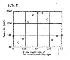
- 10 types of laser devices (11 types including the laser device in the above-described example) were produced by a method similar to the method for producing the laser device 150 in the above-described example, with only the A1 composition in the n-type current-constricting layer 109 being changed by 0.02 from 0 to 0.08 and 0.12 to 0.2. These laser devices were subjected to a similar reliability test.
- Figure 2 shows the life of the laser device with respect to the Al-mix crystal ratio of the n-type current-constricting layer 109 under the conditions of the atmospheric temperature of 60°C and the optical output of 30 mW.
- the thermal expansion coefficient of the AlGaN materials tends to increase as the Al-mix crystal ratio increases. Where the Al-mix crystal ratio is x , the thermal expansion coefficient is generally about 5 ⁇ 10 -8 ⁇ (x)/°C.
- the difference in the thermal expansion coefficient between the material forming the ridge corners 112 (p-type lower cladding layer 105 ) and the material covering and embedding the ridge corners 112 (n-type current-constricting layer 109 ) is preferably in the range of ⁇ 2 ⁇ 10 -9 /°C.
- Al 0.1 Ga 0.9 N was used for the p-type lower cladding layer 105 .
- the Al-mix crystal ratio can be appropriately set in the range of 0.05 or more and 0.3 or less.
- the refractive index of the p-type lower cladding layer 105 and the refractive index of the p-type upper cladding layer 107 are substantially equal to the refractive index of the n-type current-constricting layer 109 .
- an In 0.1 Ga 0.9 N layer was used as the p-type optical waveguide forming layer 106 .
- the In 0.1 Ga 0.9 N layer is transmissive with respect to light emitted by the multi-layer quantum well active layer 103 and has a larger refractive index than that of the n-type current-constricting layer 109 .
- the laser device in this example is stable in a single transverse mode and can oscillate light at a high output up to 30 mW.
- the wavefront of the laser beam can be substantially plane, and the astigmatic difference can be suppressed to 3 ⁇ m or less, which causes no problem in practical use.
- the method for producing the laser device 150 in this example when a physical reaction by ion irradiation such as RIE or the like is used as at least a part of the etching function for forming the ridge stripe portion 110 , it is very difficult to leave the unetched portion of the p-type lower cladding layer 105 (flat region) to have a uniform thickness with a satisfactory controllability to realize a dispersion in the order of 0.01 ⁇ m. There is an undesirable possibility that the characteristics of the laser optical waveguide are significantly varied by the non-uniformity in the thickness.
- the Al-mix crystal ratio of the p-type lower cladding layer 105 is made substantially equal to the Al-mix crystal ratio of the n-type current-constricting layer 109 .
- the etching depth i.e., the thickness of the flat region 111
- laser devices having substantially equal characteristics can be produced.
- the composition of the p-type lower cladding layer 105 and the composition of the n-type current-constricting layer 109 are different, and therefore a dispersion in the thickness of the flat region 111 of the p-type lower cladding layer 105 significantly influences the characteristics of the optical waveguide.
- the characteristics of the laser optical waveguide in this example are substantially determined by the distance between the multi-layer quantum well active layer 103 and the p-type optical waveguide forming layer 106 , the thickness or composition of these two layers, or the composition(s) of the layer(s) provided between the two layers. These parameters are all precisely controllable in the first step of crystal growth. This also provides the following effects.
- the reliability of the laser device can be improved by the reduction in the thermal distortion at the ridge corners 112 , and the yield of the InGaAlN-based semiconductor laser devices using RIE as a main etching means is greatly improved.
- the yield of devices having satisfactory initial characteristics is 24%.
- the yield is improved to 67%.
- the thickness of the p-type optical waveguide forming layer 106 in this example is 0.15 ⁇ m.
- the thickness is changed in the range from 0.03 ⁇ m to 1.5 ⁇ m, laser devices which are satisfactory both in the life and the astigmatic difference are obtained.
- the thickness of the p-type optical waveguide forming layer 106 is less than 0.03 ⁇ m, the effective refractive index of the ridge stripe portion 110 is substantially equal to that of the lower flat region 111 (the difference in the effective refractive index between the ridge stripe portion 110 and the lower flat region 111 is 1 ⁇ 10 -3 or less, 0 or less).
- the waveguide mechanism is mainly like gain guide.
- the astigmatic difference is as large as 10 ⁇ m or more, which causes the problems that the beam cannot be focused to a diffraction limit and that the oscillation in a stable fundamental transverse mode is not realized at a high output.
- the thickness of the p-type optical waveguide forming layer 106 is more than 1.5 ⁇ m, the waveguided laser light is concentrated on the p-type optical waveguide forming layer 106 . Therefore, the laser light intensity in the multi-layer quantum well active layer 103 is relatively reduced, thereby raising the threshold current value; and the total height of the ridge stripe portion 110 , which is a current path having a width of as narrow as 2 ⁇ m, becomes 2 ⁇ m or more, thereby raising the device resistance to 20 ⁇ or more. Due to these two phenomena, the life of the device is reduced to less than 100 hours.
- the distance between the p-type optical waveguide forming layer 106 and the multi-layer quantum well active layer 103 is 0.475 ⁇ m.
- the distance can be in any range to which light generated by the multi-layer quantum well active layer 103 expands. Specifically, the distance can be in the range of 0.2 ⁇ m to 1 ⁇ m.
- the p-type optical waveguide forming layer 106 can have any composition which does not absorb light generated by the multi-layer quantum well active layer 103 and which has a refractive index larger than that of the current-constricting layer 109 .
- the In-mix crystal ratio thereof is not limited to 0.1 as described in this example.
- In 0.2 Ga 0.8 N is used as the well layers of the multi-layer quantum well active layer 103 .
- the In-mix crystal ratio of the p-type optical waveguide forming layer 106 can be anything in the range of 0.02 or more and 0.18 or less.
- the p-type optical waveguide forming layer 106 absorbs the light generated in the multi-layer quantum well active layer 103 and the effective refractive index in the ridge stripe portion 110 is smaller than that of the lower flat region 111 . Therefore, the threshold current value of the laser device is increased, which causes an inconvenience that, for example, the wavefront of the output laser light is curved.
- the In-mix crystal ratio of the well layers of the multi-layer quantum well active layer 103 is changed, a similar effect is provided as long as the p-type optical waveguide forming layer 106 is formed so as to have an In-mix crystal ratio which is 90% or less with respect to that of the well layer.
- the crystal breakage occurring in the crystal growth step of the p-type upper cladding layer 107 can be reduced. This is a result of the crystal distortion between the p-type lower cladding layer 105 and the p-type upper cladding layer being alleviated by the p-type optical waveguide forming layer 106 formed of InGaN.
- the p-type optical waveguide forming layer 106 can be formed of AlGaN having a smaller Al-mix crystal ratio than that of the n-type current-constricting layer 109 , instead of InGaN. In this case, however, the effect of suppressing the crystal breakage in the p-type upper cladding layer 107 cannot be observed.
- a gallium nitride-based semiconductor laser having a long life and outputting light having a plane wavefront can be realized.
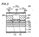
- Figure 3 shows a structure of a laser device in this example.
- the structure is the same as that of the first example until the n-type Al 0.1 Ga 0.9 N cladding layer 101 was formed.
- an n-type In 0.05 Ga 0.95 N optical guide layer 202 having a thickness of 0.05 ⁇ m
- a multi-layer quantum well active layer 203 including two Ino.2,Gag.nN well layers and one In 0.03 Ga 0.97 N barrier layer
- a p-type In 0.09 Ga 0.95 N optical waveguide layer 204 having a thickness of 0.1 ⁇ m
- a p-type Al 0.13 Ga 0.87 N cladding layer 205 having a thickness of 0.35 ⁇ m
- a p-type GaN contact layer 208 having a thickness of 1.0 ⁇ m were formed by an MOCVD technique.
- etching was performed in a manner similar to that of the first example, thereby forming a ridge structure having a width of 1.6 ⁇ m and a height of 1.2 ⁇ m. At this point, the dispersion in the etching depth was ⁇ 0.1 ⁇ m. Then, an i-type super-lattice current-constricting layer 209 including 35 pairs of an Al 0.2 Ga 0.8 N layer having a thickness of 20 nm and containing no impurity and a GaN layer having a thickness of 10 nm was selectively formed on the lower flat region 111 of the p-type cladding layer 205 by a similar method to that in the first example.
- the Al 0.2 Ga 0.5 N layers and the GaN layers were formed alternately, and the i-type super-lattice current-constricting layer 209 was formed to have a total thickness of 1.1 ⁇ m. Finally, the mask for selective growing was removed, and then a p-type GaN surface layer 2081 having a thickness of 0.3 ⁇ m was formed on the entirety of the laminate.
- n-type GaN substrate 100 was ground so that the n-type GaN substrate 100 has a thickness of 30 ⁇ m, and then polished so as to remove grinding scratches.
- an n-type electrode 113 (similar to that in the first example) was formed on the entire bottom surface of the n-type GaN substrate.
- a p-type electrode 214 was formed on a top surface of the p-type GaN surface layer 2081 .
- the resultant laminate was cleaved to have a resonator length of 450 ⁇ m, thereby producing a laser device 250.
- the i-type super-lattice current-constricting layer 209 has a super-lattice structure.
- the average Al-mix crystal ratio thereof was controlled to be substantially the same as that of the p-type cladding layer 205 formed of Al 0.19 Ga 0.87 N.
- the p-type GaN contact layer 208 is provided 0.4 ⁇ m away from the multi-layer quantum well active layer 203 and is formed of GaN which has a refractive index higher than the average refractive index of the i-type super-lattice current-constricting layer 209 . Accordingly, the laser light expands into the p-type contact layer.
- the laser light waveguide is realized in the ridge stripe portion 110 in a similar manner to that of the p-type light waveguide forming layer 106 in the first example.
- the semiconductor laser device 250 in this example was subjected to a reliability test under the conditions of 60°C and 30 mW.
- the life of the device was 10200 hours, which was a significant improvement as compared to the conventional example.
- the wavefront of the laser light is substantially plane, and the astigmatism is within 3 ⁇ m, which is sufficiently small to be free of problems in practical use.
- the Al-mix crystal ratio of the p-type cladding layer 205 and the average Al-mix crystal ratio of the i-type super-lattice current-constricting layer 209 are substantially the same as each other. Accordingly, even though the etching depth for forming the ridge stripe portion 110 is dispersed ( ⁇ 0.1 ⁇ m in this example), the difference in the effective refractive index between an area of the optical waveguide corresponding to the ridge stripe portion 110 and an area of the optical waveguide corresponding to the lower flat region 111 does not change. Accordingly, the dispersion in far-field images is reduced, and the device oscillates at a stable fundamental transverse mode up to a high output. Thus, the production yield of the device is improved. The production yield of satisfactory devices is 69% in this case.
- the p-type GaN contact layer 208 corresponding to the optical waveguide forming layer 106 in the first example is formed of GaN, which has a refractive index smaller than that of the p-type optical waveguide layer 204 .
- the device can oscillate at a threshold current value which is about 5 to 10 mA lower than that of the case where these layers have the same refractive index. As a result, a higher reliability can be realized.
- the super-lattice structured AlGaN layer for forming the i-type super-lattice current-constricting layer 209 and the GaN layer each preferably have a thickness of 50 nm or less in any case.
- the reason is that when the thickness of the super-lattice structure is 50 nm or less, the influence of the super-lattice layer on the ridge corners 112 can be considered based on the average composition of the super-lattice structure.
- the layer having the super-lattice structure has a thickness of more than 50 nm, the life is only less than 100 hours, which is similar to that of the conventional example.
- the n-type cladding layer 101 and the p-type cladding layer 205 in the second example were each replaced with a super-lattice cladding layer having a thickness of 0.45 ⁇ m.
- the super-lattice cladding layer includes 30 pairs of an Al 0.2 Ga 0.6 N layer having a thickness of 10 nm and a GaN layer having a thickness of 5 nm.
- the average Al-mix crystal ratio of the p-type cladding layer 205 and the average Al-mix crystal ratio of the i-type super-lattice current-constricting layer 209 are the same.
- the entire thermal expansion coefficients of the two layers can be considered to be about the same.
- the n-type cladding layer 101 in the first example was replaced with a super-lattice layer having a total thickness of 1.0 ⁇ m.
- the super-lattice layer includes 50 pairs of an Al 0.2 Ga 0.6 N layer having a thickness of 10 nm and containing Si, and a GaN layer having a thickness of 10 nm.
- the p-type lower cladding layer 105 in the first example was replaced with a super-lattice layer having a thickness of 0.4 ⁇ m.
- the super-lattice layer includes 20 pairs of an Al 0.2 Ga 0.8 N layer having a thickness of 10 nm and containing Mg, and a GaN layer having a thickness of 10 nm.
- the p-type optical waveguide forming layer 106 in the first example was replaced with a GaN layer having a thickness of 0.2 ⁇ m and containing Mg.
- the p-type upper cladding layer 107 in the first example was replaced with a super-lattice layer having a total thickness of 0.4 ⁇ m.
- the super-lattice layer includes 20 pairs of an Al 0.2 Ga 0.8 N layer having a thickness of 10 nm and a GaN layer having a thickness of 10 nm.
- the n-type current-constricting layer 109 in the first example was replaced with a super-lattice layer having a total thickness of 1.0 ⁇ m.
- the super-lattice cladding layer includes 50 pairs of an Al 0.2 Ga 0.8 N layer having a thickness of 10 nm and containing Si, and a GaN layer having a thickness of 10 nm.
- the p-type lower cladding layer 105 forming the ridge corners 112 and the n-type current-constricting layer 109 formed so as to cover the ridge corners 112 have the same super-lattice structure. Since the average Al-mix crystal ratios of these layers are substantially the same as each other, the thermal expansion characteristics of these layers are substantially the same as each other from a macroscopic point of view. As a result, a life of 9500 hours is obtained.
- the p-type lower cladding layer 105 and the n-type super-lattice current-constricting layer 109 do not need to have the same super-lattice structure.
- the reliability of the laser device is the same as above even when only the p-type lower cladding layer 105 is replaced with a super-lattice structure including 40 pairs of an Al 0.2 Ga 0.8 N layer having a thickness of 5 nm and containing Mg and a GaN layer having a thickness of 5, nm.
- the reliability is significantly improved as compared to the conventional example by making the Al-mix crystal ratio of the layer forming the ridge corners 112 (p-type lower cladding layer 105 in this example) equal to the average Al-mix crystal ratio of the layer forming the ridge corners 112 (n-type lower current-constricting layer 109 in this example).
- Figure 5 shows a cross-sectional structure of a different example.
- This example is similar to the first example except that an angle of ridge corners 512 made between side surfaces of the ridge and the surface of the lower flat region 111 is 90 degrees or more. Accordingly, the structures and materials which are the same as those of the first example bear the same reference numerals.
- the range of the Al-mix crystal ratio of the current-constricting layer 109 at which the reliability of 1000 hours is realized can be broader than ⁇ 0.04, which is obtained in the case where the material forming the ridge corners 512 is the same as in the first example. Specifically, it was found that a life of 1000 hours or more is realized where the Al-mix crystal ratio of the current-constricting layer is in the range of ⁇ 0.08 when the ridge corners 512 is formed of Al 0.1 Ga 0.9 N and the angle of the ridge corners 512 is in the range of 100 degrees or more and 130 degrees or less.
- the reason is considered to be the following.
- the crystal defect caused by the thermal distortion generated at the ridge corners 512 is alleviated by making the angle of the ridge corners 512 100 degrees or more.
- the propagation of the defect in the direction toward the active layer 103 located below the ridge portion 110 is suppressed.
- An angle of the ridge corners 512 exceeding 130 degrees is inappropriate for the following reason. Since the inclining surface of the ridge is too gentle to set a steep refractive index difference with respect to the transverse oscillation mode, resulting in an unstable oscillation mode.
- the Al-mix crystal ratio of the current-constricting layer 109 needs to be ⁇ 0.04 as in the first example, in order to provide the laser device with a life of 1000 hours. From the above, it was found that when the angle of the ridge corners 512 is 90 degrees or more and less than 100 degrees, the difference in the thermal expansion coefficient between the lower cladding layer 105 and the current-constricting layer 109 can be ⁇ 2 ⁇ 10 -9 /°C.
- the difference in the thermal expansion coefficient between the lower cladding layer 105 and the current-constricting layer 109 can be ⁇ 4 ⁇ 10 -9 /°C.
- GaN was used for the substrate.
- the present invention is not limited to using a GaN substrate.
- a sapphire substrate used in the conventional example, an SiC substrate or the like can be used.
- the present invention encompasses a structure in which the conductivity types in the above examples are all inverted.
- a semiconductor laser having a stable oscillation mode and a small threshold current value and thus having a superior reliability can be produced at a high yield.
- the semiconductor laser device of the present invention even when the temperature of the device is locally increased in the stripe-shaped projecting structure and the vicinity thereof in which the current is injected in a concentrated manner, the thermal distortion of the device is suppressed owing to the small difference in the thermal expansion coefficient between the current-constricting layer and the second conductive layer. Therefore, a local crystal defect or crystal breakage is avoided, thus extending the life of the laser device.
- the thermal expansion coefficient which varies depending on the Al-mix crystal ratio, can be less different between the current-constricting layer and the second layer, and thus the thermal distortion of the device can be reduced.
- the refractive index of the optical waveguide forming layer can be higher than that of the flat region of the second layer on which the current-constricting layer is formed. This way, a laser device stably oscillating in a single transverse mode up to a high output can be obtained.
- the wavefront of the output laser beam is substantially plane and the astigmatic difference can be reduced
- the thermal expansion coefficients of the second conductive layer and the current-constricting layer are substantially the same, and thus the crystal deterioration at the ridge corners is suppressed. Therefore, the life of the laser device can be extended.
- the layer having the super-lattice structure By forming the layer having the super-lattice structure to have a thickness of 50 nm or less, the influence of the super-lattice layer on the ridge corners 112 can be considered based on the average composition of the super-lattice structure.
Landscapes
- Physics & Mathematics (AREA)
- Optics & Photonics (AREA)
- Engineering & Computer Science (AREA)
- Electromagnetism (AREA)
- General Physics & Mathematics (AREA)
- Chemical & Material Sciences (AREA)
- Condensed Matter Physics & Semiconductors (AREA)
- Nanotechnology (AREA)
- Geometry (AREA)
- Life Sciences & Earth Sciences (AREA)
- Biophysics (AREA)
- Crystallography & Structural Chemistry (AREA)
- Semiconductor Lasers (AREA)
Abstract
Claims (8)
- Dispositif laser à semi-conducteur (150, 250) à base de InGaAlN, comportant une première couche plane (102, 202) présentant un premier type de conductivité, une couche active plane (103, 203) disposée sur ladite première couche et ayant une bande interdite plus petite que celle de la première couche plane, et une seconde couche (105, 205) présentant un second type de conductivité, disposée sur ladite couche active (103, 203) et ayant une bande interdite plus grande que celle de la couche active (103, 203), dans lequel la seconde couche (105, 205) comprend une zone plane (111) et une structure (110) faisant saillie sous la forme d'une bande ; une couche formant guide d'onde optique (106) sous la forme d'une bande, présentant le second type de conductivité et ayant un indice de réfraction plus grand que celui de la seconde couche (105, 205) est formée uniquement sur la structure (110) faisant saillie sous la forme d'une bande ; une couche de limitation de courant (109, 209) présentant le premier type de conductivité ou ayant une résistance élevée est formée pour recouvrir une surface supérieure de la zone plane (111) de la seconde couche, une surface latérale de la structure saillante (110) de la seconde couche et une surface latérale de la couche formant guide d'onde optique (106) ; et une différence entre un coefficient de dilatation thermique de la couche de limitation de courant (109, 209) et un coefficient de dilatation thermique de la seconde couche (105, 205) est située dans la plage de -4 × 10⁻⁹/°C à +4 × 10⁻⁹/°C.
- Dispositif laser à semi-conducteur (150, 250) selon la revendication 1, dans lequel la seconde couche (105, 205) et la couche de limitation de courant (109, 209) sont constituées d'un matériau semi-conducteur à base de InGaAlN de même composition.
- Dispositif laser à semi-conducteur (150, 250) selon la revendication 2, dans lequel la seconde couche (105, 205) est constituée de AlxGa1-xN, la couche de limitation de courant (109, 209) est formée de AlyGa1-yN, et -0,08 ≤ x - y ≤ 0,08.
- Dispositif laser à semi-conducteur (150, 250) selon la revendication 3, dans lequel un angle (112, 412, 512) formé entre la zone plane (111) et un bord de la structure (110) faisant saillie sous la forme d'une bande est d'au moins 100 degrés et d'au plus 130 degrés.
- Dispositif laser à semi-conducteur (150, 250) selon la revendication 3, dans lequel un angle (112, 412, 512) formé entre la zone plane (111) et un bord de la structure (110) faisant saillie sous la forme d'une bande est d'au moins 90 degrés et d'au plus 100 degrés, et -0,04 ≤ x - y ≤ 0,04.
- Dispositif laser à semi-conducteur (150, 250) selon la revendication 2, dans lequel la couche formant guide d'onde optique (106) est constituée de InuGa1-uN, u étant égal à au moins 0,02 et à au plus 0,18, et a une proportion de cristaux mixtes-In d'au plus 90 % d'une couche de puits comprise dans la couche active (103, 203).
- Dispositif laser à semi-conducteur (150, 250) selon la revendication 1, dans lequel la seconde couche (105, 205) et/ou la couche de limitation de courant (109, 209) est/sont constituée(s) d'une structure de super-réseau à base de InGaAlN, la seconde couche (105, 205) et la couche de limitation de courant (109, 209) ayant la même proportion de cristaux mixtes moyenne.
- Dispositif laser à semi-conducteur (150, 250) selon la revendication 7, dans lequel une couche de InGaAlN comprise dans la structure de super-réseau formant la seconde couche (105, 205) ou la couche de limitation de courant (109, 209) a une épaisseur d'au plus 50 nm.
Applications Claiming Priority (3)
| Application Number | Priority Date | Filing Date | Title |
|---|---|---|---|
| JP28485798 | 1998-10-07 | ||
| JP28485798 | 1998-10-07 | ||
| PCT/JP1999/004922 WO2000021169A1 (fr) | 1998-10-07 | 1999-09-09 | Laser a semiconducteurs |
Publications (3)
| Publication Number | Publication Date |
|---|---|
| EP1120872A1 EP1120872A1 (fr) | 2001-08-01 |
| EP1120872A4 EP1120872A4 (fr) | 2005-09-21 |
| EP1120872B1 true EP1120872B1 (fr) | 2006-12-20 |
Family
ID=17683936
Family Applications (1)
| Application Number | Title | Priority Date | Filing Date |
|---|---|---|---|
| EP99943254A Expired - Lifetime EP1120872B1 (fr) | 1998-10-07 | 1999-09-09 | Laser à semiconducteur |
Country Status (5)
| Country | Link |
|---|---|
| US (1) | US6618416B1 (fr) |
| EP (1) | EP1120872B1 (fr) |
| JP (1) | JP3886030B2 (fr) |
| DE (1) | DE69934504T2 (fr) |
| WO (1) | WO2000021169A1 (fr) |
Families Citing this family (9)
| Publication number | Priority date | Publication date | Assignee | Title |
|---|---|---|---|---|
| EP1392298B1 (fr) | 2001-05-04 | 2009-02-18 | Amgen Inc. | Composes heterocycliques fondus |
| JP2004342719A (ja) * | 2003-05-14 | 2004-12-02 | Toshiba Corp | 半導体レーザ装置及びその製造方法 |
| KR20060109112A (ko) * | 2005-04-15 | 2006-10-19 | 삼성전자주식회사 | 리지부를 구비하는 반도체 레이저 다이오드 및 그 제조방법 |
| KR20070000290A (ko) * | 2005-06-27 | 2007-01-02 | 삼성전자주식회사 | 비대칭 광도파층을 지닌 반도체 레이저 다이오드 |
| US8373152B2 (en) * | 2008-03-27 | 2013-02-12 | Lg Innotek Co., Ltd. | Light-emitting element and a production method therefor |
| JP2010225844A (ja) * | 2009-03-24 | 2010-10-07 | Opnext Japan Inc | 光半導体素子 |
| JP5332955B2 (ja) * | 2009-06-29 | 2013-11-06 | 住友電気工業株式会社 | Iii族窒化物半導体レーザ |
| JP5948776B2 (ja) * | 2011-09-27 | 2016-07-06 | ソニー株式会社 | 発光素子及びその製造方法 |
| DE102017108435A1 (de) * | 2017-04-20 | 2018-10-25 | Osram Opto Semiconductors Gmbh | Halbleiterlaserdiode und Verfahren zur Herstellung einer Halbleiterlaserdiode |
Family Cites Families (16)
| Publication number | Priority date | Publication date | Assignee | Title |
|---|---|---|---|---|
| JPS58176991A (ja) | 1982-04-09 | 1983-10-17 | Sanyo Electric Co Ltd | 半導体レ−ザ |
| JPS6091692A (ja) | 1983-10-25 | 1985-05-23 | Sharp Corp | 半導体レ−ザ装置 |
| US4768201A (en) | 1984-08-06 | 1988-08-30 | Sharp Kabushiki Kaisha | Semiconductor laser array |
| JPS61113293A (ja) | 1984-11-07 | 1986-05-31 | Sharp Corp | 半導体レ−ザアレイ装置 |
| JPS63215091A (ja) | 1987-03-04 | 1988-09-07 | Matsushita Electric Ind Co Ltd | 半導体レ−ザ装置 |
| JPH01117386A (ja) | 1987-10-30 | 1989-05-10 | Seiko Epson Corp | 化合物半導体薄膜製造方法 |
| JPH02180084A (ja) | 1988-12-29 | 1990-07-12 | Sharp Corp | 半導体レーザ素子 |
| JP3238783B2 (ja) | 1992-07-30 | 2001-12-17 | シャープ株式会社 | 半導体レーザ素子 |
| JP3429407B2 (ja) * | 1996-01-19 | 2003-07-22 | シャープ株式会社 | 半導体レーザ装置およびその製造方法 |
| JP3878707B2 (ja) | 1996-02-21 | 2007-02-07 | シャープ株式会社 | 窒化物系半導体レーザ素子の製造方法 |
| JPH09237933A (ja) | 1996-02-29 | 1997-09-09 | Mitsubishi Electric Corp | 半導体レーザ,及びその製造方法 |
| JP3688843B2 (ja) * | 1996-09-06 | 2005-08-31 | 株式会社東芝 | 窒化物系半導体素子の製造方法 |
| JP3060973B2 (ja) * | 1996-12-24 | 2000-07-10 | 日本電気株式会社 | 選択成長法を用いた窒化ガリウム系半導体レーザの製造方法及び窒化ガリウム系半導体レーザ |
| JPH10215021A (ja) * | 1997-01-30 | 1998-08-11 | Toshiba Corp | 半導体レ−ザ装置 |
| JP3957359B2 (ja) * | 1997-05-21 | 2007-08-15 | シャープ株式会社 | 窒化ガリウム系化合物半導体発光素子及びその製造方法 |
| JP3672062B2 (ja) * | 1997-07-16 | 2005-07-13 | 三菱電機株式会社 | 半導体レーザ,及びその製造方法 |
-
1999
- 1999-09-09 WO PCT/JP1999/004922 patent/WO2000021169A1/fr active IP Right Grant
- 1999-09-09 EP EP99943254A patent/EP1120872B1/fr not_active Expired - Lifetime
- 1999-09-09 DE DE69934504T patent/DE69934504T2/de not_active Expired - Lifetime
- 1999-09-09 US US09/807,003 patent/US6618416B1/en not_active Expired - Fee Related
- 1999-09-09 JP JP2000575194A patent/JP3886030B2/ja not_active Expired - Fee Related
Also Published As
| Publication number | Publication date |
|---|---|
| US6618416B1 (en) | 2003-09-09 |
| EP1120872A4 (fr) | 2005-09-21 |
| EP1120872A1 (fr) | 2001-08-01 |
| DE69934504T2 (de) | 2007-10-04 |
| WO2000021169A1 (fr) | 2000-04-13 |
| JP3886030B2 (ja) | 2007-02-28 |
| DE69934504D1 (de) | 2007-02-01 |
Similar Documents
| Publication | Publication Date | Title |
|---|---|---|
| US7817692B2 (en) | Nitride semiconductor laser device having current blocking layer and method of manufacturing the same | |
| US6984841B2 (en) | Nitride semiconductor light emitting element and production thereof | |
| KR100683875B1 (ko) | 질화물 반도체 레이저소자 | |
| US8548019B2 (en) | GaN laser element | |
| US8368183B2 (en) | Nitride semiconductor device | |
| US7508001B2 (en) | Semiconductor laser device and manufacturing method thereof | |
| US5972730A (en) | Nitride based compound semiconductor light emitting device and method for producing the same | |
| KR100539289B1 (ko) | 반도체 발광 장치 및 그 제조 방법 | |
| JP3716974B2 (ja) | 半導体レーザ素子及びその製造方法 | |
| EP1120872B1 (fr) | Laser à semiconducteur | |
| JP4534435B2 (ja) | 窒化物半導体レーザ素子及びその製造方法 | |
| KR20010007396A (ko) | 반도체 레이저 | |
| JP3916584B2 (ja) | 窒化物半導体レーザ装置 | |
| JP4847682B2 (ja) | 窒化物半導体素子およびその製造方法 | |
| EP2224559B1 (fr) | Dispositif laser à semi-conducteur de nitrure | |
| US20050116243A1 (en) | Semiconductor laser device and its manufacturing method | |
| JP3414680B2 (ja) | Iii−v族窒化物半導体レーザ | |
| JP2005101536A (ja) | 窒化物半導体レーザ素子 | |
| JP2002043692A (ja) | 半導体レーザおよびその製造方法 | |
| JP4415440B2 (ja) | 半導体レーザの製造方法 | |
| JP2007305635A (ja) | 窒化物半導体発光素子 | |
| JP5277762B2 (ja) | 窒化物半導体レーザ素子の製造方法及び窒化物半導体レーザ素子 | |
| JP2006165277A (ja) | 窒化物半導体レーザ素子 | |
| JP3849876B2 (ja) | 半導体レーザ素子及びその製造方法 | |
| JP3518842B2 (ja) | 窒化ガリウム系化合物半導体レーザ |
Legal Events
| Date | Code | Title | Description |
|---|---|---|---|
| PUAI | Public reference made under article 153(3) epc to a published international application that has entered the european phase |
Free format text: ORIGINAL CODE: 0009012 |
|
| 17P | Request for examination filed |
Effective date: 20010406 |
|
| AK | Designated contracting states |
Kind code of ref document: A1 Designated state(s): AT BE CH CY DE DK ES FI FR GB GR IE IT LI LU MC NL PT SE |
|
| RBV | Designated contracting states (corrected) |
Designated state(s): DE NL |
|
| A4 | Supplementary search report drawn up and despatched |
Effective date: 20050804 |
|
| GRAP | Despatch of communication of intention to grant a patent |
Free format text: ORIGINAL CODE: EPIDOSNIGR1 |
|
| GRAS | Grant fee paid |
Free format text: ORIGINAL CODE: EPIDOSNIGR3 |
|
| GRAA | (expected) grant |
Free format text: ORIGINAL CODE: 0009210 |
|
| AK | Designated contracting states |
Kind code of ref document: B1 Designated state(s): DE NL |
|
| REF | Corresponds to: |
Ref document number: 69934504 Country of ref document: DE Date of ref document: 20070201 Kind code of ref document: P |
|
| PLBE | No opposition filed within time limit |
Free format text: ORIGINAL CODE: 0009261 |
|
| STAA | Information on the status of an ep patent application or granted ep patent |
Free format text: STATUS: NO OPPOSITION FILED WITHIN TIME LIMIT |
|
| 26N | No opposition filed |
Effective date: 20070921 |
|
| REG | Reference to a national code |
Ref country code: DE Ref legal event code: R084 Ref document number: 69934504 Country of ref document: DE |
|
| PGFP | Annual fee paid to national office [announced via postgrant information from national office to epo] |
Ref country code: DE Payment date: 20140922 Year of fee payment: 16 |
|
| REG | Reference to a national code |
Ref country code: DE Ref legal event code: R084 Ref document number: 69934504 Country of ref document: DE Effective date: 20141002 |
|
| PGFP | Annual fee paid to national office [announced via postgrant information from national office to epo] |
Ref country code: NL Payment date: 20140918 Year of fee payment: 16 |
|
| REG | Reference to a national code |
Ref country code: DE Ref legal event code: R119 Ref document number: 69934504 Country of ref document: DE |
|
| REG | Reference to a national code |
Ref country code: NL Ref legal event code: MM Effective date: 20151001 |
|
| PG25 | Lapsed in a contracting state [announced via postgrant information from national office to epo] |
Ref country code: DE Free format text: LAPSE BECAUSE OF NON-PAYMENT OF DUE FEES Effective date: 20160401 |
|
| PG25 | Lapsed in a contracting state [announced via postgrant information from national office to epo] |
Ref country code: NL Free format text: LAPSE BECAUSE OF NON-PAYMENT OF DUE FEES Effective date: 20151001 |