EP1118922A1 - Schaltungsanordnung zum Betreiben einer Last über zwei Transistoren - Google Patents
Schaltungsanordnung zum Betreiben einer Last über zwei Transistoren Download PDFInfo
- Publication number
- EP1118922A1 EP1118922A1 EP00127024A EP00127024A EP1118922A1 EP 1118922 A1 EP1118922 A1 EP 1118922A1 EP 00127024 A EP00127024 A EP 00127024A EP 00127024 A EP00127024 A EP 00127024A EP 1118922 A1 EP1118922 A1 EP 1118922A1
- Authority
- EP
- European Patent Office
- Prior art keywords
- transistor
- transistors
- voltage
- current
- load
- Prior art date
- Legal status (The legal status is an assumption and is not a legal conclusion. Google has not performed a legal analysis and makes no representation as to the accuracy of the status listed.)
- Granted
Links
- 101150109657 ureF gene Proteins 0.000 description 9
- 238000009826 distribution Methods 0.000 description 6
- 238000004146 energy storage Methods 0.000 description 3
- 230000008878 coupling Effects 0.000 description 2
- 238000010168 coupling process Methods 0.000 description 2
- 238000005859 coupling reaction Methods 0.000 description 2
- 102100033828 26S proteasome regulatory subunit 10B Human genes 0.000 description 1
- 101100390736 Danio rerio fign gene Proteins 0.000 description 1
- 101100390738 Mus musculus Fign gene Proteins 0.000 description 1
- 101150020953 PSMC6 gene Proteins 0.000 description 1
- 101100030895 Saccharomyces cerevisiae (strain ATCC 204508 / S288c) RPT4 gene Proteins 0.000 description 1
- 239000003990 capacitor Substances 0.000 description 1
- 230000001276 controlling effect Effects 0.000 description 1
- 230000000694 effects Effects 0.000 description 1
- 230000005669 field effect Effects 0.000 description 1
- 238000010438 heat treatment Methods 0.000 description 1
- 230000001939 inductive effect Effects 0.000 description 1
- 230000001105 regulatory effect Effects 0.000 description 1
- MYVIATVLJGTBFV-UHFFFAOYSA-M thiamine(1+) chloride Chemical compound [Cl-].CC1=C(CCO)SC=[N+]1CC1=CN=C(C)N=C1N MYVIATVLJGTBFV-UHFFFAOYSA-M 0.000 description 1
Images

Classifications
-
- G—PHYSICS
- G05—CONTROLLING; REGULATING
- G05F—SYSTEMS FOR REGULATING ELECTRIC OR MAGNETIC VARIABLES
- G05F1/00—Automatic systems in which deviations of an electric quantity from one or more predetermined values are detected at the output of the system and fed back to a device within the system to restore the detected quantity to its predetermined value or values, i.e. retroactive systems
- G05F1/10—Regulating voltage or current
- G05F1/46—Regulating voltage or current wherein the variable actually regulated by the final control device is DC
- G05F1/56—Regulating voltage or current wherein the variable actually regulated by the final control device is DC using semiconductor devices in series with the load as final control devices
- G05F1/565—Regulating voltage or current wherein the variable actually regulated by the final control device is DC using semiconductor devices in series with the load as final control devices sensing a condition of the system or its load in addition to means responsive to deviations in the output of the system, e.g. current, voltage, power factor
- G05F1/569—Regulating voltage or current wherein the variable actually regulated by the final control device is DC using semiconductor devices in series with the load as final control devices sensing a condition of the system or its load in addition to means responsive to deviations in the output of the system, e.g. current, voltage, power factor for protection
- G05F1/573—Regulating voltage or current wherein the variable actually regulated by the final control device is DC using semiconductor devices in series with the load as final control devices sensing a condition of the system or its load in addition to means responsive to deviations in the output of the system, e.g. current, voltage, power factor for protection with overcurrent detector
Definitions
- the invention relates to a circuit arrangement with two transistors, which in Interconnect series with a load to be operated.
- a typical example of one about one Output driven load is the electrical ignition element of the Gas generator of an automotive airbag. In this application example is about a short time a defined minimum power to ignite the electrical Ignition element implemented in this.
- the energy supply exists here essentially from an energy storage device, for example a capacitor having. To protect the driver transistors, but also to protect them before an excessive current flows through the load becomes an output stage current-limited, which is due to the use of transistors is realized with current limitation.
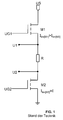
- FIG. 1 A known circuit arrangement with current limitation is shown in FIG. 1.
- Such a current-limited output stage generally exists the problem in that the electrical power dissipation on the two Transistors M1 and M2 is uneven and therefore poorly distributed.
- a load R the can be resistive, capacitive or inductive through the two transistors M1 and M2, which are bipolar or field effect transistors can, energized. Since the load R is far from the two transistors M1 and M2 can be located away to avoid damage in operation and a short-circuit protection or current limitation for the two transistors M1 and M2 required. Otherwise they would have short circuits the supply lines with the potentials U1 and U2 against a positive or negative supply damage to transistors M1 or M2 resulted.
- Limiting the current may also be necessary for the load R. For example, to avoid that at the beginning or at the end overcurrents flow in a switched-on state. It can also appear be to prevent such overcurrents because otherwise the Circuit arrangement feeding energy storage discharges itself too quickly. This should, for example, in a motor vehicle application of the circuit arrangement according to the invention for igniting the ignition elements of the gas generators multiple airbags can be prevented. That is after the collapse of the electrical system can still trigger all airbags no greater current than the ignition current is supplied to each ignition element, otherwise the energy in the energy storage will not ignite them all required airbag would be sufficient.
- the current limitation in the transistors M1 and M2 takes place in the manner known per se by means of shunt resistors or by measuring the voltage drop across the transistors or a part of these transistors. It is not physically possible for the same voltage drop and thus the same power to be set across both transistors. The reason for this can be seen in the fact that the transistors have limit currents of different magnitudes due to specimen scatter. As a result, the limitation on one of the two transistors M1, M2 will always have a stronger effect than on the other. A very large voltage drop will thus occur via one of the two transistors M1, M2, with which the far greater part of the power must be absorbed by this transistor. In the circuit arrangement according to FIG. 1 it is assumed that the current limitation over the transistor M2 is slightly smaller than over the transistor M1; in other words, I lim (M1) is greater than I lim (M2) .
- From DE-A-15 13 168 is an output stage for operating a load known, in which two transistors connected in series with one to operating load are switched. One of the two transistors is like this controlled that the current flowing over its conduction path to one Maximum value is limited.
- the invention has for its object a circuit arrangement for Operating a load via two transistors to be connected in series with the load with which it is easily possible to create the power loss distribute evenly across both transistors.
- the two transistors connected to current control circuits at their control inputs, which ensure that the conduction paths of the transistors flowing currents are limited to first or second maximum values.
- the Current limiting value of the first transistor is greater than the current limiting value of the second transistor.
- control signal at the control input of the first transistor if a current flows with the size of the second maximum value, such adjustable that a voltage across the line path of the first transistor drops that is greater than the voltage that would drop if over the conduction path of the first transistor has a current the size of the second Maximum value flows.
- Influencing the control signal at the control input of the first transistor can be done by simply returning the voltage drop across the first Transistor can be realized.
- a coupling or additional interconnection the current limiting circuits of both transistors is in the invention Circuitry not required, so that by conceivable little effort a more even distribution of the two transistors power loss to be implemented is achieved or prevented, that one of the two transistors absorb significantly more power loss has than the other.
- An advantageous further development is a comparator for comparing the voltage drop over the line path of the first transistor with a reference voltage intended. This comparator then gives when the voltage drop over the conduction path of the first transistor is larger than that Reference voltage, an output signal for influencing the first control signal for the control input of the first transistor.
- An even easier one Feedback of the voltage drop across the first transistor to its Control input is realized in that the current limiting circuit of the first transistor as a function of a reference voltage supplying first voltage source is controlled and that the first transistor is connected as a voltage follower. So that the voltage drop over the first transistor at least for a defined time or a defined Operating state does not become greater than the reference voltage, it applies So that the voltage drop across the transistor is essentially the same the reference voltage.
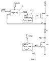
- the circuit arrangement according to FIG. 2 shows a first possibility according to the invention of an improved power distribution to the two transistors M1 and M 2 when current flows through the load R.
- the transistors or actuators are deliberately impressed with different current limits.
- the supply voltage SUG2 of the current limiting circuit CL2 for the transistor M2 is used to generate the control voltage UG2 for the transistor M2.
- This voltage is regulated in the current limiting circuit CL2 for the transistor M2 in such a way that a maximum current I lim (M2) is set via the transistor M2.
- I lim (M2) is set via the transistor M2.
- I lim (M2) is set via the transistor M2.
- I lim (M2) is greater than the current limitation for transistor M2. So the following applies: I lim (M1) is greater than I lim (M2) .
- the reference voltage UREF is freely selectable and so is the power distribution freely selectable on the two transistors M1 and M2.
- the reference voltage UREF can be made using a voltage divider from the supply voltage US generated or applied with a fixed voltage, so that when this voltage at U1 is exceeded, the voltage drop and so the power consumption is minimized or only then fully effective becomes. Combinations of fixed and proportional voltage components to UREF or a change over time is possible.
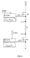
- FIG. 3 Another embodiment of the circuit arrangement according to the invention shows Fig. 3. This circuit arrangement is compared to the circuit arrangement 2 simplified to the extent that the return of the Voltage at U1 is dispensed with and that for controlling the current limiting circuit CL1 required for the transistor M1 control voltage RSUG1 2 directly from the reference voltage UREF is produced. This is achieved by switching transistor M1 as a voltage follower is. Also in the example according to FIG. 3, at least one applies Time or a defined operating state that the voltage at U1 is substantially equal to the reference voltage UREF.
- a wide range can be achieved with the circuit arrangement according to the invention of power distributions over location, working conditions (voltage) and time adjust without there being a coupling of the current limiting circuits of the two transistors M1 and M2 is required. That means the transistors M1 and M2 can be arranged locally far apart. The transistors M1 and M2 can thus be loaded in a simple manner be optimized.
- Figs. 2 and 3 circuit arrangements shown can be also add to a (full) bridge circuit.
- Fig. 4 shows such a full bridge circuit for the circuit variant according to FIG. 2. Depending on the direction of the current through the load R either flows through the pair of transistors M1, M4 or M2, M3.
Landscapes
- Engineering & Computer Science (AREA)
- Physics & Mathematics (AREA)
- Electromagnetism (AREA)
- General Physics & Mathematics (AREA)
- Radar, Positioning & Navigation (AREA)
- Automation & Control Theory (AREA)
- Electronic Switches (AREA)
- Amplifiers (AREA)
- Logic Circuits (AREA)
- Continuous-Control Power Sources That Use Transistors (AREA)
Abstract
Description
- einem ersten Transistor, der einen mit einem ersten Steuersignal beaufschlagbaren Steuereingang und einem in Abhängigkeit von dem ersten Steuersignal steuerbaren Leitungspfad aufweist, wobei der über den Leitungspfad fließende Strom auf einen ersten Maximalwert begrenzt ist.
- einem zweiten Transistor, der einen mit einem zweiten Steuersignal beaufschlagbaren Steuereingang und einem in Abhängigkeit von dem zweiten Steuersignal steuerbaren Leitungspfad aufweist, wobei der über den Leitungspfad fließende Strom auf einen zweiten Maximalwert begrenzt ist,
- wobei
- der erste Maximalwert größer ist als der zweite Maximalwert,
- die Last in Reihe mit den Leitungspfaden des ersten und des zweiten Transistors verschaltbar ist und
- bei von einem Strom mit der Größe des zweiten Maximalwerts durchflossener Last das erste Steuersignal an dem Steuereingang des ersten Transistors derart einstellbar ist, dass über den Leitungspfad des ersten Transistors eine Spannung fällt, die größer ist als diejenige Spannung, die abfällt, wenn über dem Leitungspfad des ersten Transistors ein Strom mit der Größe des zweiten Maximalwerts fließt.
- Fig. 1
- eine Schaltungsanordnung gemäß dem Stand der Technik und
- Fign. 2 bis 4
- verschiedene Ausführungsbeispiele einer erfindungsgemäßen Schaltungsanordnung zum Betreiben einer Last über zwei mit der Last in Reihe zu schaltende Transistoren.
Ilim(M1) ist größer als Ilim(M2).
Claims (3)
- Schaltungsanordnung zum Betreiben einer Last über zwei mit der Last in Reihe zu schaltende Transistoren, miteinem ersten Transistor (M1), der einen mit einem ersten Steuersignal beaufschlagbaren Steuereingang und einem in Abhängigkeit von dem ersten Steuersignal steuerbaren Leitungspfad aufweist, wobei der über den Leitungspfad fließende Strom auf einen ersten Maximalwert (Ilim(M1)) begrenzt ist.einem zweiten Transistor (M2), der einen mit einem zweiten Steuersignal beaufschlagbaren Steuereingang und einem in Abhängigkeit von dem zweiten Steuersignal steuerbaren Leitungspfad aufweist, wobei der über den Leitungspfad fließende Strom auf einen zweiten Maximalwert (Ilim(M2)) begrenzt ist,wobeider erste Maximalwert (Ilim(M1)) größer ist als der zweite Maximalwert (Ilim(M2)),die Last (R) in Reihe mit den Leitungspfaden des ersten und des zweiten Transistors (M1,M2) verschaltbar ist undbei von einem Strom mit der Größe des zweiten Maximalwerts durchflossener Last (R) das erste Steuersignal an dem Steuereingang des ersten Transistors (M1) derart einstellbar ist, dass über den Leitungspfad des ersten Transistors (M1) eine Spannung abfällt, die größer ist als diejenige Spannung, die abfällt, wenn über dem Leitungspfad des ersten Transistors (M1) ein Strom mit der Größe des zweiten Maximalwerts fließt.
- Schaltungsanordnung nach Anspruch 1, dadurch gekennzeichnet, dass ein Vergleicher C1 zum Vergleich des Spannungsabfalls über dem Leitungspfad des ersten Transistors (M1) mit einer Referenzspannung vorgesehen ist und dass der Vergleicher C1 dann, wenn der Spannungsabfall größer ist als die Referenzspannung, ein Ausgangssignal zur Beeinflussung des ersten Steuersignals für den Steuereingang des ersten Transistors (M1) ausgibt.
- Schaltungsanordnung nach Anspruch 1, dadurch gekennzeichnet, dass das erste Steuersignal am Steuereingang des ersten Transistors (M1) in Abhängigkeit von einer eine Referenzspannung liefernden externen Spannungsquelle einstellbar ist und dass der erste Transistor (M1) als Spannungsfolger geschaltet ist.
Applications Claiming Priority (2)
| Application Number | Priority Date | Filing Date | Title |
|---|---|---|---|
| DE10002037A DE10002037C1 (de) | 2000-01-19 | 2000-01-19 | Schaltungsanordnung zum Betreiben einer Last über zwei Transistoren |
| DE10002037 | 2000-01-19 |
Publications (2)
| Publication Number | Publication Date |
|---|---|
| EP1118922A1 true EP1118922A1 (de) | 2001-07-25 |
| EP1118922B1 EP1118922B1 (de) | 2003-07-09 |
Family
ID=7627962
Family Applications (1)
| Application Number | Title | Priority Date | Filing Date |
|---|---|---|---|
| EP00127024A Expired - Lifetime EP1118922B1 (de) | 2000-01-19 | 2000-12-09 | Schaltungsanordnung zum Betreiben einer Last über zwei Transistoren |
Country Status (4)
| Country | Link |
|---|---|
| US (1) | US6337587B2 (de) |
| EP (1) | EP1118922B1 (de) |
| AT (1) | ATE244906T1 (de) |
| DE (2) | DE10002037C1 (de) |
Families Citing this family (4)
| Publication number | Priority date | Publication date | Assignee | Title |
|---|---|---|---|---|
| DE19841445C2 (de) * | 1998-09-10 | 2002-04-25 | Infineon Technologies Ag | Halbleiter-Schaltungsanordnung |
| DE10049774C2 (de) * | 2000-09-29 | 2002-11-07 | Infineon Technologies Ag | Gegentaktendstufe für digitale Signale mit geregelten Ausgangspegeln |
| JP2002290221A (ja) * | 2001-03-27 | 2002-10-04 | Nec Corp | 半導体出力回路の消費電力低減回路 |
| JP4323756B2 (ja) * | 2002-05-01 | 2009-09-02 | キヤノン株式会社 | 記録装置 |
Citations (4)
| Publication number | Priority date | Publication date | Assignee | Title |
|---|---|---|---|---|
| GB937506A (en) * | 1960-12-01 | 1963-09-25 | Westinghouse Brake & Signal | Improvements relating to power transistors and voltage regulating circuits therefor |
| CH389039A (de) * | 1961-07-20 | 1965-03-15 | Standard Telephon & Radio Ag | Spannungsstabilisierte Gleichstromspeiseeinrichtung |
| GB1105259A (en) * | 1964-12-10 | 1968-03-06 | Goerz Electro Gmbh | A voltage stabilising circuit |
| JPS59128617A (ja) * | 1983-01-12 | 1984-07-24 | Matsushita Electric Ind Co Ltd | 電流出力装置 |
Family Cites Families (4)
| Publication number | Priority date | Publication date | Assignee | Title |
|---|---|---|---|---|
| JP2990889B2 (ja) * | 1991-09-27 | 1999-12-13 | 日本電気株式会社 | 磁気ヘッドドライブ回路 |
| EP0782268B1 (de) * | 1995-12-29 | 2002-04-24 | STMicroelectronics S.r.l. | Schaltkreis für Betriebsspannungen |
| JP2000268309A (ja) * | 1999-03-19 | 2000-09-29 | Mitsubishi Electric Corp | 書き込み電流駆動回路 |
| US6262620B1 (en) * | 1999-11-02 | 2001-07-17 | Ranco Incorporated Of Delaware | Driver circuitry for latching type valve and the like |
-
2000
- 2000-01-19 DE DE10002037A patent/DE10002037C1/de not_active Expired - Fee Related
- 2000-12-09 AT AT00127024T patent/ATE244906T1/de not_active IP Right Cessation
- 2000-12-09 DE DE50002823T patent/DE50002823D1/de not_active Expired - Lifetime
- 2000-12-09 EP EP00127024A patent/EP1118922B1/de not_active Expired - Lifetime
-
2001
- 2001-01-19 US US09/764,206 patent/US6337587B2/en not_active Expired - Lifetime
Patent Citations (4)
| Publication number | Priority date | Publication date | Assignee | Title |
|---|---|---|---|---|
| GB937506A (en) * | 1960-12-01 | 1963-09-25 | Westinghouse Brake & Signal | Improvements relating to power transistors and voltage regulating circuits therefor |
| CH389039A (de) * | 1961-07-20 | 1965-03-15 | Standard Telephon & Radio Ag | Spannungsstabilisierte Gleichstromspeiseeinrichtung |
| GB1105259A (en) * | 1964-12-10 | 1968-03-06 | Goerz Electro Gmbh | A voltage stabilising circuit |
| JPS59128617A (ja) * | 1983-01-12 | 1984-07-24 | Matsushita Electric Ind Co Ltd | 電流出力装置 |
Non-Patent Citations (1)
| Title |
|---|
| PATENT ABSTRACTS OF JAPAN vol. 008, no. 259 (P - 317) 28 November 1984 (1984-11-28) * |
Also Published As
| Publication number | Publication date |
|---|---|
| US6337587B2 (en) | 2002-01-08 |
| ATE244906T1 (de) | 2003-07-15 |
| EP1118922B1 (de) | 2003-07-09 |
| US20010008380A1 (en) | 2001-07-19 |
| DE50002823D1 (de) | 2003-08-14 |
| DE10002037C1 (de) | 2001-08-23 |
Similar Documents
| Publication | Publication Date | Title |
|---|---|---|
| DE3341345C2 (de) | Längsspannungsregler | |
| DE19817767A1 (de) | Halbleiter-Leistungsschaltung | |
| DE102014108576B4 (de) | Treiberschaltung mit Miller-Clamping-Funktionalität für Leistungshalbleiterschalter, Leistungshalbleiterschalter und Wechselrichterbrücke | |
| DE69604761T2 (de) | Stromversorgung für einen Mikrorechner | |
| DE102004062032A1 (de) | Schaltungsanordnung zur schnellen Reduzierung eines induzierten Stroms | |
| DE102006054354A1 (de) | Selbstschützende Crowbar | |
| DE3842288A1 (de) | Schaltungsanordnung zur erzeugung einer konstanten bezugsspannung | |
| EP0973084B1 (de) | Integrierte Schaltung mit einem Spannungsregler | |
| DE102004062205A1 (de) | Schaltungsanordnung und Verfahren zum Schutz einer Schaltung vor elektrostatischen Entladungen | |
| EP1118922B1 (de) | Schaltungsanordnung zum Betreiben einer Last über zwei Transistoren | |
| EP0374288B1 (de) | Integrierbare Schaltungsanordnung zur Rückstromverringerung bei einem invers betriebenen Transistor | |
| EP0957420B1 (de) | Klemmschaltung | |
| EP0876699B1 (de) | Strombegrenzungsschaltung | |
| DE69812755T2 (de) | Schutzschaltung gegen Kurzschlüsse | |
| DE102010010103B3 (de) | Elektronische Vorrichtung zur Steuerung eines Stroms | |
| DE2202894A1 (de) | Stromversorgungseinrichtung fuer elektronische Anlagen | |
| DE102014001264B4 (de) | Präzisionsstrombegrenzung und Überstromabschaltung zum Schutz eines monolithisch integrierten Treibers mittels einer adapiven Referenzerzeugung | |
| EP1038355B1 (de) | Pufferschaltung | |
| DE10349629B4 (de) | Elektronischer Schaltkreis | |
| DE2404850C3 (de) | Elektronische Sicherung für einen Gegentakt-Verstarker | |
| DD277562A1 (de) | Schaltung zur strombegrenzung mit foldback-verhalten | |
| DE3891380C2 (de) | Verstärker mit vier Transistoren, die in einer Brückenschaltung miteinander verbunden sind | |
| DE2529883B1 (de) | Schaltungsanordnung zum UEberlastungsschutz | |
| DE3906955C1 (en) | Electronic fuse (safety device) for a transistor output stage | |
| DE102006054547B4 (de) | Chip mit einer Schaltungsanordnung zur Spannungsregelung |
Legal Events
| Date | Code | Title | Description |
|---|---|---|---|
| PUAI | Public reference made under article 153(3) epc to a published international application that has entered the european phase |
Free format text: ORIGINAL CODE: 0009012 |
|
| AK | Designated contracting states |
Kind code of ref document: A1 Designated state(s): AT BE CH CY DE DK ES FI FR GB GR IE IT LI LU MC NL PT SE TR |
|
| AX | Request for extension of the european patent |
Free format text: AL;LT;LV;MK;RO;SI |
|
| 17P | Request for examination filed |
Effective date: 20010824 |
|
| 17Q | First examination report despatched |
Effective date: 20011025 |
|
| AKX | Designation fees paid |
Free format text: AT BE CH CY DE DK ES FI FR GB GR IE IT LI LU MC NL PT SE TR |
|
| GRAH | Despatch of communication of intention to grant a patent |
Free format text: ORIGINAL CODE: EPIDOS IGRA |
|
| GRAH | Despatch of communication of intention to grant a patent |
Free format text: ORIGINAL CODE: EPIDOS IGRA |
|
| GRAA | (expected) grant |
Free format text: ORIGINAL CODE: 0009210 |
|
| AK | Designated contracting states |
Designated state(s): AT BE CH CY DE DK ES FI FR GB GR IE IT LI LU MC NL PT SE TR |
|
| PG25 | Lapsed in a contracting state [announced via postgrant information from national office to epo] |
Ref country code: TR Free format text: LAPSE BECAUSE OF FAILURE TO SUBMIT A TRANSLATION OF THE DESCRIPTION OR TO PAY THE FEE WITHIN THE PRESCRIBED TIME-LIMIT Effective date: 20030709 Ref country code: FI Free format text: LAPSE BECAUSE OF FAILURE TO SUBMIT A TRANSLATION OF THE DESCRIPTION OR TO PAY THE FEE WITHIN THE PRESCRIBED TIME-LIMIT Effective date: 20030709 |
|
| REG | Reference to a national code |
Ref country code: GB Ref legal event code: FG4D Free format text: NOT ENGLISH |
|
| REG | Reference to a national code |
Ref country code: CH Ref legal event code: EP |
|
| REF | Corresponds to: |
Ref document number: 50002823 Country of ref document: DE Date of ref document: 20030814 Kind code of ref document: P |
|
| REG | Reference to a national code |
Ref country code: CH Ref legal event code: NV Representative=s name: HEPP, WENGER & RYFFEL AG |
|
| REG | Reference to a national code |
Ref country code: IE Ref legal event code: FG4D Free format text: GERMAN |
|
| PG25 | Lapsed in a contracting state [announced via postgrant information from national office to epo] |
Ref country code: GR Free format text: LAPSE BECAUSE OF FAILURE TO SUBMIT A TRANSLATION OF THE DESCRIPTION OR TO PAY THE FEE WITHIN THE PRESCRIBED TIME-LIMIT Effective date: 20031009 Ref country code: DK Free format text: LAPSE BECAUSE OF FAILURE TO SUBMIT A TRANSLATION OF THE DESCRIPTION OR TO PAY THE FEE WITHIN THE PRESCRIBED TIME-LIMIT Effective date: 20031009 Ref country code: SE Free format text: LAPSE BECAUSE OF FAILURE TO SUBMIT A TRANSLATION OF THE DESCRIPTION OR TO PAY THE FEE WITHIN THE PRESCRIBED TIME-LIMIT Effective date: 20031009 |
|
| PG25 | Lapsed in a contracting state [announced via postgrant information from national office to epo] |
Ref country code: ES Free format text: LAPSE BECAUSE OF FAILURE TO SUBMIT A TRANSLATION OF THE DESCRIPTION OR TO PAY THE FEE WITHIN THE PRESCRIBED TIME-LIMIT Effective date: 20031020 |
|
| GBT | Gb: translation of ep patent filed (gb section 77(6)(a)/1977) |
Effective date: 20031110 |
|
| PG25 | Lapsed in a contracting state [announced via postgrant information from national office to epo] |
Ref country code: CY Free format text: LAPSE BECAUSE OF FAILURE TO SUBMIT A TRANSLATION OF THE DESCRIPTION OR TO PAY THE FEE WITHIN THE PRESCRIBED TIME-LIMIT Effective date: 20031209 Ref country code: LU Free format text: LAPSE BECAUSE OF NON-PAYMENT OF DUE FEES Effective date: 20031209 Ref country code: PT Free format text: LAPSE BECAUSE OF FAILURE TO SUBMIT A TRANSLATION OF THE DESCRIPTION OR TO PAY THE FEE WITHIN THE PRESCRIBED TIME-LIMIT Effective date: 20031209 |
|
| PG25 | Lapsed in a contracting state [announced via postgrant information from national office to epo] |
Ref country code: MC Free format text: LAPSE BECAUSE OF NON-PAYMENT OF DUE FEES Effective date: 20031231 |
|
| ET | Fr: translation filed | ||
| PLBE | No opposition filed within time limit |
Free format text: ORIGINAL CODE: 0009261 |
|
| STAA | Information on the status of an ep patent application or granted ep patent |
Free format text: STATUS: NO OPPOSITION FILED WITHIN TIME LIMIT |
|
| 26N | No opposition filed |
Effective date: 20040414 |
|
| PGFP | Annual fee paid to national office [announced via postgrant information from national office to epo] |
Ref country code: CH Payment date: 20081222 Year of fee payment: 9 Ref country code: IE Payment date: 20081218 Year of fee payment: 9 Ref country code: NL Payment date: 20081219 Year of fee payment: 9 |
|
| PGFP | Annual fee paid to national office [announced via postgrant information from national office to epo] |
Ref country code: AT Payment date: 20081218 Year of fee payment: 9 |
|
| PGFP | Annual fee paid to national office [announced via postgrant information from national office to epo] |
Ref country code: IT Payment date: 20081223 Year of fee payment: 9 |
|
| PGFP | Annual fee paid to national office [announced via postgrant information from national office to epo] |
Ref country code: FR Payment date: 20081216 Year of fee payment: 9 |
|
| PGFP | Annual fee paid to national office [announced via postgrant information from national office to epo] |
Ref country code: GB Payment date: 20081219 Year of fee payment: 9 |
|
| PGFP | Annual fee paid to national office [announced via postgrant information from national office to epo] |
Ref country code: BE Payment date: 20090107 Year of fee payment: 9 |
|
| BERE | Be: lapsed |
Owner name: *ELMOS SEMICONDUCTOR A.G. Effective date: 20091231 |
|
| REG | Reference to a national code |
Ref country code: NL Ref legal event code: V1 Effective date: 20100701 |
|
| REG | Reference to a national code |
Ref country code: CH Ref legal event code: PL |
|
| GBPC | Gb: european patent ceased through non-payment of renewal fee |
Effective date: 20091209 |
|
| PG25 | Lapsed in a contracting state [announced via postgrant information from national office to epo] |
Ref country code: AT Free format text: LAPSE BECAUSE OF NON-PAYMENT OF DUE FEES Effective date: 20091209 |
|
| REG | Reference to a national code |
Ref country code: FR Ref legal event code: ST Effective date: 20100831 |
|
| REG | Reference to a national code |
Ref country code: IE Ref legal event code: MM4A |
|
| PG25 | Lapsed in a contracting state [announced via postgrant information from national office to epo] |
Ref country code: LI Free format text: LAPSE BECAUSE OF NON-PAYMENT OF DUE FEES Effective date: 20091231 Ref country code: FR Free format text: LAPSE BECAUSE OF NON-PAYMENT OF DUE FEES Effective date: 20091231 Ref country code: BE Free format text: LAPSE BECAUSE OF NON-PAYMENT OF DUE FEES Effective date: 20091231 Ref country code: CH Free format text: LAPSE BECAUSE OF NON-PAYMENT OF DUE FEES Effective date: 20091231 Ref country code: IE Free format text: LAPSE BECAUSE OF NON-PAYMENT OF DUE FEES Effective date: 20091209 Ref country code: NL Free format text: LAPSE BECAUSE OF NON-PAYMENT OF DUE FEES Effective date: 20100701 |
|
| PG25 | Lapsed in a contracting state [announced via postgrant information from national office to epo] |
Ref country code: GB Free format text: LAPSE BECAUSE OF NON-PAYMENT OF DUE FEES Effective date: 20091209 |
|
| PG25 | Lapsed in a contracting state [announced via postgrant information from national office to epo] |
Ref country code: IT Free format text: LAPSE BECAUSE OF NON-PAYMENT OF DUE FEES Effective date: 20091209 |
|
| REG | Reference to a national code |
Ref country code: DE Ref legal event code: R082 Ref document number: 50002823 Country of ref document: DE Representative=s name: VON KREISLER SELTING WERNER - PARTNERSCHAFT VO, DE |
|
| REG | Reference to a national code |
Ref country code: DE Ref legal event code: R082 Ref document number: 50002823 Country of ref document: DE Representative=s name: DOMPATENT VON KREISLER SELTING WERNER - PARTNE, DE Effective date: 20150108 Ref country code: DE Ref legal event code: R082 Ref document number: 50002823 Country of ref document: DE Representative=s name: VON KREISLER SELTING WERNER - PARTNERSCHAFT VO, DE Effective date: 20150108 Ref country code: DE Ref legal event code: R081 Ref document number: 50002823 Country of ref document: DE Owner name: ELMOS SEMICONDUCTOR AKTIENGESELLSCHAFT, DE Free format text: FORMER OWNER: ELMOS SEMICONDUCTOR AG, 44227 DORTMUND, DE Effective date: 20150108 |
|
| PGFP | Annual fee paid to national office [announced via postgrant information from national office to epo] |
Ref country code: DE Payment date: 20191217 Year of fee payment: 20 |
|
| REG | Reference to a national code |
Ref country code: DE Ref legal event code: R082 Ref document number: 50002823 Country of ref document: DE Representative=s name: DOMPATENT VON KREISLER SELTING WERNER - PARTNE, DE Ref country code: DE Ref legal event code: R081 Ref document number: 50002823 Country of ref document: DE Owner name: ELMOS SEMICONDUCTOR SE, DE Free format text: FORMER OWNER: ELMOS SEMICONDUCTOR AKTIENGESELLSCHAFT, 44227 DORTMUND, DE |
|
| REG | Reference to a national code |
Ref country code: DE Ref legal event code: R071 Ref document number: 50002823 Country of ref document: DE |