EP1113499A2 - High fill factor image array having a continuous amorphous silicon sensor layer and a doped poly-silicon back contact - Google Patents
High fill factor image array having a continuous amorphous silicon sensor layer and a doped poly-silicon back contact Download PDFInfo
- Publication number
- EP1113499A2 EP1113499A2 EP00311111A EP00311111A EP1113499A2 EP 1113499 A2 EP1113499 A2 EP 1113499A2 EP 00311111 A EP00311111 A EP 00311111A EP 00311111 A EP00311111 A EP 00311111A EP 1113499 A2 EP1113499 A2 EP 1113499A2
- Authority
- EP
- European Patent Office
- Prior art keywords
- amorphous silicon
- back contact
- layer
- silicon layer
- doped
- Prior art date
- Legal status (The legal status is an assumption and is not a legal conclusion. Google has not performed a legal analysis and makes no representation as to the accuracy of the status listed.)
- Granted
Links
- 229910021417 amorphous silicon Inorganic materials 0.000 title claims abstract description 72
- 229910021420 polycrystalline silicon Inorganic materials 0.000 title claims abstract description 19
- 238000000034 method Methods 0.000 claims abstract description 18
- 235000001674 Agaricus brunnescens Nutrition 0.000 claims description 16
- 239000004020 conductor Substances 0.000 claims description 11
- XUIMIQQOPSSXEZ-UHFFFAOYSA-N Silicon Chemical compound [Si] XUIMIQQOPSSXEZ-UHFFFAOYSA-N 0.000 claims description 6
- 229910052755 nonmetal Inorganic materials 0.000 claims description 6
- 229910052710 silicon Inorganic materials 0.000 claims description 6
- 239000010703 silicon Substances 0.000 claims description 6
- 230000015572 biosynthetic process Effects 0.000 claims description 5
- 238000000151 deposition Methods 0.000 claims description 5
- 238000005499 laser crystallization Methods 0.000 claims description 4
- 238000001514 detection method Methods 0.000 claims description 3
- 230000005684 electric field Effects 0.000 claims description 3
- 238000002161 passivation Methods 0.000 claims description 3
- 239000002210 silicon-based material Substances 0.000 claims 1
- 239000002184 metal Substances 0.000 abstract description 44
- 239000000463 material Substances 0.000 abstract description 11
- 238000002347 injection Methods 0.000 description 15
- 239000007924 injection Substances 0.000 description 15
- 230000004888 barrier function Effects 0.000 description 8
- HBMJWWWQQXIZIP-UHFFFAOYSA-N silicon carbide Chemical compound [Si+]#[C-] HBMJWWWQQXIZIP-UHFFFAOYSA-N 0.000 description 5
- 229910010271 silicon carbide Inorganic materials 0.000 description 4
- 238000004519 manufacturing process Methods 0.000 description 3
- XYFCBTPGUUZFHI-UHFFFAOYSA-N Phosphine Chemical compound P XYFCBTPGUUZFHI-UHFFFAOYSA-N 0.000 description 2
- 230000008901 benefit Effects 0.000 description 2
- 238000010586 diagram Methods 0.000 description 2
- 239000010408 film Substances 0.000 description 2
- 238000005468 ion implantation Methods 0.000 description 2
- 229910021424 microcrystalline silicon Inorganic materials 0.000 description 2
- OAICVXFJPJFONN-UHFFFAOYSA-N Phosphorus Chemical group [P] OAICVXFJPJFONN-UHFFFAOYSA-N 0.000 description 1
- BLRPTPMANUNPDV-UHFFFAOYSA-N Silane Chemical compound [SiH4] BLRPTPMANUNPDV-UHFFFAOYSA-N 0.000 description 1
- 229910000577 Silicon-germanium Inorganic materials 0.000 description 1
- 238000003491 array Methods 0.000 description 1
- 230000003139 buffering effect Effects 0.000 description 1
- 238000005229 chemical vapour deposition Methods 0.000 description 1
- 229910021419 crystalline silicon Inorganic materials 0.000 description 1
- 230000000593 degrading effect Effects 0.000 description 1
- 230000008021 deposition Effects 0.000 description 1
- 230000009977 dual effect Effects 0.000 description 1
- 238000005516 engineering process Methods 0.000 description 1
- 239000003574 free electron Substances 0.000 description 1
- 229910052739 hydrogen Inorganic materials 0.000 description 1
- 239000001257 hydrogen Substances 0.000 description 1
- 125000004435 hydrogen atom Chemical class [H]* 0.000 description 1
- 238000005984 hydrogenation reaction Methods 0.000 description 1
- 238000003384 imaging method Methods 0.000 description 1
- 150000002500 ions Chemical class 0.000 description 1
- 238000002844 melting Methods 0.000 description 1
- 230000008018 melting Effects 0.000 description 1
- 150000004706 metal oxides Chemical group 0.000 description 1
- 229910000073 phosphorus hydride Inorganic materials 0.000 description 1
- 238000005036 potential barrier Methods 0.000 description 1
- 230000000717 retained effect Effects 0.000 description 1
- 238000007789 sealing Methods 0.000 description 1
- 239000004065 semiconductor Substances 0.000 description 1
- 229910000077 silane Inorganic materials 0.000 description 1
- 239000010409 thin film Substances 0.000 description 1
Images



Classifications
-
- H—ELECTRICITY
- H10—SEMICONDUCTOR DEVICES; ELECTRIC SOLID-STATE DEVICES NOT OTHERWISE PROVIDED FOR
- H10F—INORGANIC SEMICONDUCTOR DEVICES SENSITIVE TO INFRARED RADIATION, LIGHT, ELECTROMAGNETIC RADIATION OF SHORTER WAVELENGTH OR CORPUSCULAR RADIATION
- H10F39/00—Integrated devices, or assemblies of multiple devices, comprising at least one element covered by group H10F30/00, e.g. radiation detectors comprising photodiode arrays
- H10F39/80—Constructional details of image sensors
- H10F39/802—Geometry or disposition of elements in pixels, e.g. address-lines or gate electrodes
-
- H—ELECTRICITY
- H10—SEMICONDUCTOR DEVICES; ELECTRIC SOLID-STATE DEVICES NOT OTHERWISE PROVIDED FOR
- H10F—INORGANIC SEMICONDUCTOR DEVICES SENSITIVE TO INFRARED RADIATION, LIGHT, ELECTROMAGNETIC RADIATION OF SHORTER WAVELENGTH OR CORPUSCULAR RADIATION
- H10F39/00—Integrated devices, or assemblies of multiple devices, comprising at least one element covered by group H10F30/00, e.g. radiation detectors comprising photodiode arrays
- H10F39/10—Integrated devices
- H10F39/12—Image sensors
- H10F39/191—Photoconductor image sensors
-
- Y—GENERAL TAGGING OF NEW TECHNOLOGICAL DEVELOPMENTS; GENERAL TAGGING OF CROSS-SECTIONAL TECHNOLOGIES SPANNING OVER SEVERAL SECTIONS OF THE IPC; TECHNICAL SUBJECTS COVERED BY FORMER USPC CROSS-REFERENCE ART COLLECTIONS [XRACs] AND DIGESTS
- Y02—TECHNOLOGIES OR APPLICATIONS FOR MITIGATION OR ADAPTATION AGAINST CLIMATE CHANGE
- Y02E—REDUCTION OF GREENHOUSE GAS [GHG] EMISSIONS, RELATED TO ENERGY GENERATION, TRANSMISSION OR DISTRIBUTION
- Y02E10/00—Energy generation through renewable energy sources
- Y02E10/50—Photovoltaic [PV] energy
- Y02E10/548—Amorphous silicon PV cells
Definitions
- the present invention relates generally to the structure of a high fill factor image array with a continuous sensor layer and its method of manufacture.
- Vertical leakage current also degrades image quality by introducing noise.
- the introduced noise reduces image contrast and/or gray scale.
- a typical 60X60 square micrometer of a PIN sensor may include about 20 femto-amps (fA) of intrinsic leakage current at five volt contact voltages.
- vertical leakage currents reduce image contrast thereby degrading the quality of images output.
- One source of vertical leakage current is a contact injection current that results when a metal comes in contact with intrinsic amorphous silicon.
- a single mask is used to form both the metal back contact and an N+ doped amorphous silicon layer over the metal contact.
- the use of a single mask for both the N+ doped amorphous silicon layer and the metal back contact results in an edge of the metal being exposed to the intrinsic amorphous silicon.
- the area is sufficient to generate a large amount of vertical leakage current.
- one embodiment of the invention uses a second mask to generate a wider N+ amorphous silicon layer that seals in the metal portion of the back contact and prevents all direct contact between the intrinsic amorphous silicon layer and the metal back contact.
- An alternative embodiment of the invention replaces both the metal back contact and the N+ amorphous silicon layer with a single alternative material such as an N+ doped poly-silicon contact. Still a third embodiment of the invention retains the N+ amorphous silicon layer and replaces only the metal back contact with another conducting material that does not generate significant injection current when brought into contact with intrinsic amorphous silicon.
- Fig. 1 shows a sensor structure in which an N+ doped amorphous silicon layer completely eliminates contact between a metal back contact and an intrinsic amorphous silicon layer.
- a “back contact” is defined as a sensor contact that is designed to increase charge collection from a sensor medium, such as amorphous silicon, by increasing the surface area of a charge collecting surface.
- a sensor medium such as amorphous silicon
- Such back contacts are “mushroom shaped” to provided a larger surface area on a side exposed to the sensor medium and a smaller contact point surface area that couples the collected charge to detection electronics.
- a center portion of the mushroom shape typically forms a "U” with the bottom of the "U” forming the contact point and extensions from the top of the "U” providing additional surface area to collect charge.
- the extensions are typically oriented perpendicular to the top of the "U” and parallel to the collection surface.
- a P+ doped amorphous silicon layer 52, an intrinsic silicon layer 50, and an N+ doped amorphous silicon layer 48 together form a PIN structure.
- metal back contact 46 is mushroom shaped to from a metal mushroom contact.
- a mushroom shaped contact typically includes a "U" shaped portion including a conducting bottom segment 65 and two conducting upright segments 67, 69.
- a first end of each upright segment 67, 69 is coupled to corresponding ends of bottom segment 65.
- Each upright segment 67, 69 is oriented approximately perpendicular to bottom segment 65.
- a second end of each upright conducting segment 67, 69 is coupled to an end of a corresponding conducting extension segment 71, 73.
- Each, extension segment 71, 73 is oriented approximately parallel to bottom segment 65 and approximately perpendicular to upright conducting segments 67, 69.
- each mushroom contact includes a larger charge collection surface 49 created by extension segments 71, 73.
- Charge collection surface 49 receives charge from the sensor medium.
- a contact point 51 transfers the collected charge from the mushroom contact to underlying electronics via line 104.
- Line 104 couples the charge to support or readout electronics.
- line 104 is a data line that couples to a gate of a thin film transistor TFT transistor 108.
- TFT transistor 108 may be formed using a number of different methods.
- One method of integrating the sensor with detection or imaging electronics that include TFT transistor 108 is to form the TFT transistor from a Complimentary Metal Oxide Structure (CMOS) and to form the sensor medium including the amorphous silicon layer 50 directly over the CMOS electronics.
- CMOS Complimentary Metal Oxide Structure
- a reference that describes the formation of a CMOS structure for use in a sensor is "Image Sensors in TFA Technology- Status and Future Trends" by Bohm, M. et al. presented on Pages 327-338 of the conference paper of the Amorphous and Microcrystalline Silicon Technology 1998 Symposium held in San Francisco on April 14-17, 1988.
- one embodiment of the invention uses a first mask to form the metal back contact and a second mask to form the N+ amorphous silicon layer.
- the area of the N+ amorphous silicon layer is slightly larger than the area of the metal back contact to create an overhang area 120 of N+ amorphous silicon that covers the edges 112, 116 of metal back contact 46.
- the overhang area 120 eliminates the direct contact between metal and intrinsic amorphous silicon by sealing off metal portions of the back contact from the intrinsic amorphous silicon.
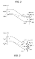
- Fig. 2 illustrates the Fermi level of a reverse biased PIN amorphous silicon to metal interface while Fig. 3 illustrates the Fermi level of a PI amorphous silicon to metal Schottky interface.
- a dark reverse-bias current results from 1) bulk generation, 2) contact injection and 3) edge leakage.
- the contact injection portion of the dark reverse bias current arises from carrier injection across a junction barrier between a metal electrode and the amorphous silicon.
- the energy band profile or Fermi level 200 is relatively flat.
- the barrier height 220 for hole generation, ⁇ is the potential difference near interface 208 between a Fermi level 200 in the N+ layer and the valence band 204 in the N+ layer.
- Fig. 3 illustrates a Schottky diode in which an intrinsic amorphous silicon contacts a metal.
- the Fermi level 304 in the intrinsic amorphous silicon layer spreads slightly but is typically pinned at a center of bandgap 308 near the silicon to metal interface 312.
- the junction barrier height for hole generation, ⁇ is the potential difference between Fermi level 304 and valence band 316 near the silicon to metal interface 312.
- Fig. 3. and Fig. 2 together illustrate that the Schottky diode barrier height 320 is significantly smaller than the barrier height 220 when a heavily doped N+ layer interfaces with a metal. The smaller barrier height results in a larger injection current.
- Fig. 4 plots the injection current density in a Schottky diode as a function of an applied bias voltage.
- the current density is plotted along vertical axis 408 and the bias voltage is plotted along horizontal axis 404.
- Each curve 412, 416, 420, 424 plots the current density versus bias voltage characteristic for a different type of metal.
- the metal can be removed in Fig. 1 leaving only the N+ amorphous layer deposited in a mushroom form.
- the sheet resistance of N doped amorphous silicon is high, typically on the order of 6 MegaOhms per square. The high sheet resistance slows down read-out time.
- Fig. 5 illustrates one embodiment of the invention in which both the metal back contact 46 and the N doped silicon layer 48 of Fig. 1 are replaced by a single N doped poly-silicon back contact 504.
- the poly-silicon back contact 504 serves as a good conductor to collect and transport charge to line 104.
- the N doping of poly-silicon back contact 504 also provides the desired PIN structure. As illustrated, the poly-silicon back contact 504 also maintains a mushroom shape.
- One method of formation includes depositing an N doped amorphous silicon layer in a mushroom configuration. Laser Crystallization converts the N doped amorphous silicon layer into an N doped poly-silicon layer.
- a selective laser process may be used that does not completely melt the N doped amorphous silicon. Complete melting of the amorphous silicon is not needed to achieve the low resistance desired as will be illustrated in the graph of Fig. 6.
- Passivation layer 56 also serves as a buffering layer further protecting TFT 108.
- Fig. 6 is a graph that shows the change in sheet resistivity of a 100 nanometer section of amorphous silicon doped with phosphor atoms as a function of laser exposure. Sheet resistivity is plotted along vertical axis 604 while laser energy density is plotted along horizontal axis 608.
- a second method of forming a doped poly-silicon back contact includes depositing intrinsic amorphous silicon. Ion implantation or laser doping is used to deposit N+ ions in the intrinsic amorphous silicon. A laser anneal after the ion implantation or laser doping converts the amorphous silicon into poly-silicon. Poly-silicon back contact 504 may be exposed to several minutes of plasma hydrogenation prior to deposition of intrinsic amorphous silicon to assure a high quality n-i junction 508 between the poly-silicon and the intrinsic amorphous silicon.
- Alternate materials besides poly-Silicon may be used to replace the combination of metal back contact 46 and N+ doped amorphous silicon layer 48 of Fig. 1.
- One example of such a material is doped micro-crystalline Silicon.
- a PECVD ( Plasma Enhance Chemical Vapor Deposition) process may be used to deposit the doped miro-crystalline silicon with hydrogen dilute silane and phosphine.
- Another suitable material is doped poly-SiC (poly-silicon carbide).
- poly-SiC poly-silicon carbide
- One benefit of using poly-SiC is that the wide energy band gap of the poly-SiC provides a high potential barrier that reduces hole injection and minimizes contact current.
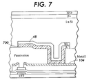
- Fig. 7 illustrates an alternate embodiment of the invention that continues to utilize two layers for a mushroom contact, including the N+ amorphous silicon layer 48 of Fig. 1.
- a substitute material 700 Suitable substitute materials should be a semiconductor conductor with a low sheet resistance (lower than 100 kilo Ohms per square) which allows direct contact with the intrinsic amorphous silicon layer without generating large amounts of contact current.
- Suitable substitute materials include doped poly-silicon, doped SiC, doped SiGe and doped Ge films.
- the dual structure of an N+ layer and a substitute material maintains the nature of an amorphous silicon PIN junction while utilizing the substitute material to conduct charge and minimize contact injection current. Because some contact with the intrinsic amorphous silicon is allowed, a single mask is used in the fabrication of both the N doped amorphous silicon layer and the substitute material of the back contact.
Landscapes
- Solid State Image Pick-Up Elements (AREA)
- Transforming Light Signals Into Electric Signals (AREA)
- Light Receiving Elements (AREA)
Abstract
Description
Claims (10)
- A sensor comprising:an intrinsic amorphous silicon layer;a p doped silicon layer coupled to a first side of the intrinsic amorphous silicon layer;a transparent first electrode coupled to the p doped silicon layer; and,at least one nonmetallic back contact coupled to a second side of the intrinsic amorphous layer, the back contact to collect charge from an area of the intrinsic amorphous silicon layer and to provide the collected charge to detection electronics.
- A sensor according to claim 1, wherein the back contact is formed in a mushroom shape comprising:a bottom conducting segment;two upright conducting segments, a first end of each upright conducting segment coupled to a corresponding end of the bottom conducting segment, each upright conducting segment oriented approximately perpendicular to the bottom conducting segment; andat least one extension segment coupled to a second end of an upright conducting segment.
- A sensor according to claim 1 or 2, wherein the nonmetallic back contact is an N doped poly-silicon material.
- A sensor according to any one of the preceding claims, further comprising:
an N doped layer of amorphous silicon positioned between the intrinsic amorphous silicon layer and the nonmetallic back contact. - A sensor according to any one of the preceding claims, further comprising:
a passivation layer separating the nonmetallic back contact from an adjacent nonmetallic back contact. - A method of forming a sensor comprising the operations of:depositing a non-metal conductor over a passivation layer and a conducting line to form a back contact;forming an intrinsic amorphous silicon layer over the non-metal conductor, the intrinsic amorphous silicon layer to generate electrons from incident photons;forming a transparent conductor over the intrinsic amorphous silicon layer, the transparent conductor and the non-metal conductor to apply an electric field across the intrinsic amorphous silicon.
- A method according to claim 6, further comprising the operation of:forming a P+ amorphous silicon layer between the intrinsic amorphous silicon layer and the transparent conductor.
- A method according to claim 6 or 7, wherein the non-metal conductor has a sheet resistivity below 100 ohms.
- A method according to claim 6, 7 or 8, wherein the formation of the non-metal conductor comprises the operation of:depositing a N doped layer of amorphous silicon; andusing a laser crystallization process to convert the N doped layer of amorphous silicon to a layer of N doped poly-silicon.
- A method according to claim 9, wherein the laser energy density used in the laser crystallization is between 150 and 700 mJ/cm2.
Applications Claiming Priority (2)
| Application Number | Priority Date | Filing Date | Title |
|---|---|---|---|
| US473578 | 1999-12-28 | ||
| US09/473,578 US6288435B1 (en) | 1999-12-28 | 1999-12-28 | Continuous amorphous silicon layer sensors using doped poly-silicon back contact |
Publications (3)
| Publication Number | Publication Date |
|---|---|
| EP1113499A2 true EP1113499A2 (en) | 2001-07-04 |
| EP1113499A3 EP1113499A3 (en) | 2003-04-16 |
| EP1113499B1 EP1113499B1 (en) | 2007-07-25 |
Family
ID=23880139
Family Applications (1)
| Application Number | Title | Priority Date | Filing Date |
|---|---|---|---|
| EP00311111A Expired - Lifetime EP1113499B1 (en) | 1999-12-28 | 2000-12-13 | High fill factor image array having a continuous amorphous silicon sensor layer and a doped poly-silicon back contact and fabrication method |
Country Status (4)
| Country | Link |
|---|---|
| US (1) | US6288435B1 (en) |
| EP (1) | EP1113499B1 (en) |
| JP (2) | JP2001250935A (en) |
| DE (1) | DE60035665T2 (en) |
Cited By (6)
| Publication number | Priority date | Publication date | Assignee | Title |
|---|---|---|---|---|
| WO2003038901A1 (en) * | 2001-10-26 | 2003-05-08 | Stmicroelectronics Nv | Method for producing a tfa image sensor and one such tfa image sensor |
| EP1326278A3 (en) * | 2002-01-07 | 2004-03-10 | Xerox Corporation | Image sensor with performance enhancing structures |
| EP1677354A1 (en) * | 2004-12-30 | 2006-07-05 | DongbuAnam Semiconductor Inc. | CMOS image sensor and method for manufacturing the same |
| US7282382B2 (en) | 2001-10-29 | 2007-10-16 | Stmicroelectronics N.V. | Method for producing a photodiode contact for a TFA image sensor |
| GB2442997A (en) * | 2006-10-20 | 2008-04-23 | Pei Sung Chuang | An image integrated circuit |
| EP2270859A3 (en) * | 2009-07-03 | 2012-08-08 | Sony Corporation | Photoelectric conversion apparatus and radiographic imaging apparatus |
Families Citing this family (36)
| Publication number | Priority date | Publication date | Assignee | Title |
|---|---|---|---|---|
| US6730914B2 (en) * | 2002-02-05 | 2004-05-04 | E-Phocus, Inc. | Photoconductor-on-active-pixel (POAP) sensor utilizing equal-potential pixel electrodes |
| US7214945B2 (en) * | 2002-06-11 | 2007-05-08 | Canon Kabushiki Kaisha | Radiation detecting apparatus, manufacturing method therefor, and radiation image pickup system |
| US7670936B1 (en) * | 2002-10-18 | 2010-03-02 | Advanced Micro Devices, Inc. | Nitridation of gate oxide by laser processing |
| JP2004343031A (en) * | 2002-12-03 | 2004-12-02 | Advanced Lcd Technologies Development Center Co Ltd | Dielectric film, method of forming the same, semiconductor device using dielectric film and method of manufacturing the same |
| US7067891B2 (en) * | 2003-11-04 | 2006-06-27 | Taiwan Semiconductor Manufacturing Co., Ltd. | Sensor element having elevated diode with sidewall passivated bottom electrode |
| KR100884204B1 (en) | 2007-07-19 | 2009-02-18 | 주식회사 동부하이텍 | Image sensor and its manufacturing method |
| KR100877293B1 (en) | 2007-08-31 | 2009-01-07 | 주식회사 동부하이텍 | Image sensor and its manufacturing method |
| KR101329352B1 (en) * | 2007-10-17 | 2013-11-13 | 삼성전자주식회사 | Method for manufacturing of semiconductor device |
| TWI415283B (en) * | 2009-02-18 | 2013-11-11 | Au Optronics Corp | X-ray sensor and manufacturing method thereof |
| US9570678B1 (en) | 2010-06-08 | 2017-02-14 | Crossbar, Inc. | Resistive RAM with preferental filament formation region and methods |
| US9601692B1 (en) | 2010-07-13 | 2017-03-21 | Crossbar, Inc. | Hetero-switching layer in a RRAM device and method |
| US8946046B1 (en) | 2012-05-02 | 2015-02-03 | Crossbar, Inc. | Guided path for forming a conductive filament in RRAM |
| US8168506B2 (en) | 2010-07-13 | 2012-05-01 | Crossbar, Inc. | On/off ratio for non-volatile memory device and method |
| US8884261B2 (en) | 2010-08-23 | 2014-11-11 | Crossbar, Inc. | Device switching using layered device structure |
| US8569172B1 (en) | 2012-08-14 | 2013-10-29 | Crossbar, Inc. | Noble metal/non-noble metal electrode for RRAM applications |
| JP2012039004A (en) * | 2010-08-10 | 2012-02-23 | Sony Corp | Photoelectric conversion element and method of manufacturing the same |
| US8492195B2 (en) | 2010-08-23 | 2013-07-23 | Crossbar, Inc. | Method for forming stackable non-volatile resistive switching memory devices |
| US8391049B2 (en) * | 2010-09-29 | 2013-03-05 | Crossbar, Inc. | Resistor structure for a non-volatile memory device and method |
| US8558212B2 (en) | 2010-09-29 | 2013-10-15 | Crossbar, Inc. | Conductive path in switching material in a resistive random access memory device and control |
| USRE46335E1 (en) | 2010-11-04 | 2017-03-07 | Crossbar, Inc. | Switching device having a non-linear element |
| US8502185B2 (en) | 2011-05-31 | 2013-08-06 | Crossbar, Inc. | Switching device having a non-linear element |
| US9620206B2 (en) | 2011-05-31 | 2017-04-11 | Crossbar, Inc. | Memory array architecture with two-terminal memory cells |
| US8619459B1 (en) | 2011-06-23 | 2013-12-31 | Crossbar, Inc. | High operating speed resistive random access memory |
| US9564587B1 (en) | 2011-06-30 | 2017-02-07 | Crossbar, Inc. | Three-dimensional two-terminal memory with enhanced electric field and segmented interconnects |
| US9166163B2 (en) | 2011-06-30 | 2015-10-20 | Crossbar, Inc. | Sub-oxide interface layer for two-terminal memory |
| US9627443B2 (en) | 2011-06-30 | 2017-04-18 | Crossbar, Inc. | Three-dimensional oblique two-terminal memory with enhanced electric field |
| US8946669B1 (en) | 2012-04-05 | 2015-02-03 | Crossbar, Inc. | Resistive memory device and fabrication methods |
| CN103828047A (en) | 2011-07-22 | 2014-05-28 | 科洛斯巴股份有限公司 | Seed layer for a p + silicon germanium material for non-volatile memory device and method |
| US9685608B2 (en) | 2012-04-13 | 2017-06-20 | Crossbar, Inc. | Reduced diffusion in metal electrode for two-terminal memory |
| US8658476B1 (en) | 2012-04-20 | 2014-02-25 | Crossbar, Inc. | Low temperature P+ polycrystalline silicon material for non-volatile memory device |
| US9583701B1 (en) | 2012-08-14 | 2017-02-28 | Crossbar, Inc. | Methods for fabricating resistive memory device switching material using ion implantation |
| US10096653B2 (en) | 2012-08-14 | 2018-10-09 | Crossbar, Inc. | Monolithically integrated resistive memory using integrated-circuit foundry compatible processes |
| US8946673B1 (en) | 2012-08-24 | 2015-02-03 | Crossbar, Inc. | Resistive switching device structure with improved data retention for non-volatile memory device and method |
| US9312483B2 (en) | 2012-09-24 | 2016-04-12 | Crossbar, Inc. | Electrode structure for a non-volatile memory device and method |
| US9576616B2 (en) | 2012-10-10 | 2017-02-21 | Crossbar, Inc. | Non-volatile memory with overwrite capability and low write amplification |
| US10290801B2 (en) | 2014-02-07 | 2019-05-14 | Crossbar, Inc. | Scalable silicon based resistive memory device |
Family Cites Families (17)
| Publication number | Priority date | Publication date | Assignee | Title |
|---|---|---|---|---|
| JPS60189379A (en) * | 1984-03-08 | 1985-09-26 | Matsushita Electric Ind Co Ltd | Solid-state image pickup device |
| JPS60206064A (en) * | 1984-03-30 | 1985-10-17 | Toshiba Corp | Manufacture of solid-state image pickup device |
| JPS62193277A (en) * | 1986-02-20 | 1987-08-25 | Toshiba Corp | Solid-state image pickup device |
| JPS62264657A (en) * | 1986-05-13 | 1987-11-17 | Toshiba Corp | Solid-state image sensing device and manufacture thereof |
| JPS6450465A (en) * | 1987-08-20 | 1989-02-27 | Canon Kk | Semiconductor device |
| JPH01138752A (en) * | 1987-11-26 | 1989-05-31 | Toshiba Corp | Laminated solid-state image sensing device |
| JPH02109362A (en) * | 1988-10-18 | 1990-04-23 | Fujitsu Ltd | Laminated solid-state image sensing element |
| JP2624318B2 (en) * | 1988-11-25 | 1997-06-25 | 三菱電機株式会社 | Image sensor and method of manufacturing the same |
| JPH03174772A (en) * | 1989-09-29 | 1991-07-29 | Toshiba Corp | Solid-state image pickup device |
| JPH04103168A (en) * | 1990-08-23 | 1992-04-06 | Sony Corp | Solid-state image sensing element |
| JPH04216670A (en) * | 1990-12-17 | 1992-08-06 | Canon Inc | Photoelectric transducer |
| JPH04261070A (en) * | 1991-01-11 | 1992-09-17 | Canon Inc | Photoelectric conversion device |
| IT1277856B1 (en) * | 1995-02-09 | 1997-11-12 | Univ Roma | ULTRAVIOLET RADIATION DETECTOR IN THIN FILM, WITH HIGH SPECTRAL SELECTIVITY OPTION. |
| US5619033A (en) * | 1995-06-07 | 1997-04-08 | Xerox Corporation | Layered solid state photodiode sensor array |
| GB9520791D0 (en) * | 1995-10-13 | 1995-12-13 | Philips Electronics Nv | Image sensor |
| US6114739A (en) * | 1998-10-19 | 2000-09-05 | Agilent Technologies | Elevated pin diode active pixel sensor which includes a patterned doped semiconductor electrode |
| JP3794193B2 (en) * | 1999-03-04 | 2006-07-05 | シャープ株式会社 | Liquid crystal display element, manufacturing method thereof, and liquid crystal display device |
-
1999
- 1999-12-28 US US09/473,578 patent/US6288435B1/en not_active Expired - Lifetime
-
2000
- 2000-12-13 EP EP00311111A patent/EP1113499B1/en not_active Expired - Lifetime
- 2000-12-13 DE DE60035665T patent/DE60035665T2/en not_active Expired - Lifetime
- 2000-12-28 JP JP2000400871A patent/JP2001250935A/en active Pending
-
2012
- 2012-05-14 JP JP2012110835A patent/JP5280564B2/en not_active Expired - Lifetime
Cited By (10)
| Publication number | Priority date | Publication date | Assignee | Title |
|---|---|---|---|---|
| WO2003038901A1 (en) * | 2001-10-26 | 2003-05-08 | Stmicroelectronics Nv | Method for producing a tfa image sensor and one such tfa image sensor |
| US7326589B2 (en) | 2001-10-26 | 2008-02-05 | Stmicroelectronics N.V. | Method for producing a TFA image sensor and one such TFA image sensor |
| US7282382B2 (en) | 2001-10-29 | 2007-10-16 | Stmicroelectronics N.V. | Method for producing a photodiode contact for a TFA image sensor |
| EP1326278A3 (en) * | 2002-01-07 | 2004-03-10 | Xerox Corporation | Image sensor with performance enhancing structures |
| EP1677354A1 (en) * | 2004-12-30 | 2006-07-05 | DongbuAnam Semiconductor Inc. | CMOS image sensor and method for manufacturing the same |
| US7442572B2 (en) | 2004-12-30 | 2008-10-28 | Dongbu Electronic Co., Ltd. | CMOS image sensor and method for manufacturing the same |
| US7745862B2 (en) | 2004-12-30 | 2010-06-29 | Dongbu Electronics Co., Ltd. | CMOS image sensor and method for manufacturing the same |
| GB2442997A (en) * | 2006-10-20 | 2008-04-23 | Pei Sung Chuang | An image integrated circuit |
| EP2270859A3 (en) * | 2009-07-03 | 2012-08-08 | Sony Corporation | Photoelectric conversion apparatus and radiographic imaging apparatus |
| US9136296B2 (en) | 2009-07-03 | 2015-09-15 | Sony Corporation | Photoelectric conversion apparatus and radiographic imaging apparatus |
Also Published As
| Publication number | Publication date |
|---|---|
| JP2001250935A (en) | 2001-09-14 |
| JP2012199563A (en) | 2012-10-18 |
| DE60035665D1 (en) | 2007-09-06 |
| EP1113499A3 (en) | 2003-04-16 |
| DE60035665T2 (en) | 2008-05-21 |
| JP5280564B2 (en) | 2013-09-04 |
| EP1113499B1 (en) | 2007-07-25 |
| US6288435B1 (en) | 2001-09-11 |
Similar Documents
| Publication | Publication Date | Title |
|---|---|---|
| EP1113499B1 (en) | High fill factor image array having a continuous amorphous silicon sensor layer and a doped poly-silicon back contact and fabrication method | |
| KR102143468B1 (en) | Electromagnetic radiation detector based on wafer bonding | |
| US6300648B1 (en) | Continuous amorphous silicon layer sensors using sealed metal back contact | |
| EP0165764B1 (en) | Depletion mode thin film semiconductor photodetectors | |
| US5677201A (en) | Laminated solid-state image pickup device and a method for manufacturing the same | |
| EP1009038A2 (en) | Radiation detecting apparatus | |
| JP2000188386A (en) | Manufacturing method of two-dimensional image detector | |
| EP0428050B1 (en) | Photosensor having an amorphous silicon photoabsorption layer | |
| EP0211720B1 (en) | Method for making a light image sensor, and bidimensional sensor array made by this method | |
| EP0178148A2 (en) | Thin film photodetector | |
| US4499654A (en) | Method for fabricating semiconductor photodetector | |
| WO2021192296A1 (en) | Electromagnetic wave detector, electromagnetic wave detector array, and manufacturing method of electromagnetic wave detector | |
| US4714950A (en) | Solid-state photo sensor device | |
| US5942788A (en) | Solid state image sensing device | |
| JPS6211792B2 (en) | ||
| Sudharsanan et al. | CdZnTe photodiode arrays for medical imaging | |
| Wronski et al. | Charge transfer enhancement of photoconductivity in hydrogenated amorphous Ge/Si multilayer films | |
| JPS59143379A (en) | Photoconductor and its manufacturing method | |
| JPH0652428B2 (en) | Photoconductor | |
| JPH04261070A (en) | Photoelectric conversion device | |
| Park et al. | Process Integration of A-Si: H Schottky Diode and thin Film Transistor for Low-Energy X-Ray Imaging Applications | |
| JPS6322465B2 (en) | ||
| JPH05259496A (en) | Semiconductor radiation detector | |
| JP2002246577A (en) | X-ray image detector | |
| Tao et al. | Large Area Digital X‐ray Imaging |
Legal Events
| Date | Code | Title | Description |
|---|---|---|---|
| PUAI | Public reference made under article 153(3) epc to a published international application that has entered the european phase |
Free format text: ORIGINAL CODE: 0009012 |
|
| AK | Designated contracting states |
Kind code of ref document: A2 Designated state(s): AT BE CH CY DE DK ES FI FR GB GR IE IT LI LU MC NL PT SE TR |
|
| AX | Request for extension of the european patent |
Free format text: AL;LT;LV;MK;RO;SI |
|
| PUAL | Search report despatched |
Free format text: ORIGINAL CODE: 0009013 |
|
| RIC1 | Information provided on ipc code assigned before grant |
Ipc: 7H 01L 31/18 B Ipc: 7H 01L 27/146 A |
|
| AK | Designated contracting states |
Designated state(s): AT BE CH CY DE DK ES FI FR GB GR IE IT LI LU MC NL PT SE TR |
|
| AX | Request for extension of the european patent |
Extension state: AL LT LV MK RO SI |
|
| 17P | Request for examination filed |
Effective date: 20031016 |
|
| AKX | Designation fees paid |
Designated state(s): DE FR GB |
|
| 17Q | First examination report despatched |
Effective date: 20051220 |
|
| 17Q | First examination report despatched |
Effective date: 20051220 |
|
| GRAP | Despatch of communication of intention to grant a patent |
Free format text: ORIGINAL CODE: EPIDOSNIGR1 |
|
| RTI1 | Title (correction) |
Free format text: HIGH FILL FACTOR IMAGE ARRAY HAVING A CONTINUOUS AMORPHOUS SILICON SENSOR LAYER AND A DOPED POLY-SILICON BACK CONTACT AND FABRICATION METHOD |
|
| GRAS | Grant fee paid |
Free format text: ORIGINAL CODE: EPIDOSNIGR3 |
|
| GRAA | (expected) grant |
Free format text: ORIGINAL CODE: 0009210 |
|
| AK | Designated contracting states |
Kind code of ref document: B1 Designated state(s): DE FR GB |
|
| REG | Reference to a national code |
Ref country code: GB Ref legal event code: FG4D |
|
| REF | Corresponds to: |
Ref document number: 60035665 Country of ref document: DE Date of ref document: 20070906 Kind code of ref document: P |
|
| ET | Fr: translation filed | ||
| PLBE | No opposition filed within time limit |
Free format text: ORIGINAL CODE: 0009261 |
|
| STAA | Information on the status of an ep patent application or granted ep patent |
Free format text: STATUS: NO OPPOSITION FILED WITHIN TIME LIMIT |
|
| 26N | No opposition filed |
Effective date: 20080428 |
|
| REG | Reference to a national code |
Ref country code: FR Ref legal event code: PLFP Year of fee payment: 16 |
|
| REG | Reference to a national code |
Ref country code: FR Ref legal event code: PLFP Year of fee payment: 17 |
|
| REG | Reference to a national code |
Ref country code: FR Ref legal event code: PLFP Year of fee payment: 18 |
|
| PGFP | Annual fee paid to national office [announced via postgrant information from national office to epo] |
Ref country code: DE Payment date: 20171120 Year of fee payment: 18 Ref country code: FR Payment date: 20171121 Year of fee payment: 18 |
|
| PGFP | Annual fee paid to national office [announced via postgrant information from national office to epo] |
Ref country code: GB Payment date: 20171121 Year of fee payment: 18 |
|
| REG | Reference to a national code |
Ref country code: DE Ref legal event code: R119 Ref document number: 60035665 Country of ref document: DE |
|
| GBPC | Gb: european patent ceased through non-payment of renewal fee |
Effective date: 20181213 |
|
| PG25 | Lapsed in a contracting state [announced via postgrant information from national office to epo] |
Ref country code: DE Free format text: LAPSE BECAUSE OF NON-PAYMENT OF DUE FEES Effective date: 20190702 Ref country code: FR Free format text: LAPSE BECAUSE OF NON-PAYMENT OF DUE FEES Effective date: 20181231 |
|
| PG25 | Lapsed in a contracting state [announced via postgrant information from national office to epo] |
Ref country code: GB Free format text: LAPSE BECAUSE OF NON-PAYMENT OF DUE FEES Effective date: 20181213 |