EP1009038A2 - Radiation detecting apparatus - Google Patents
Radiation detecting apparatus Download PDFInfo
- Publication number
- EP1009038A2 EP1009038A2 EP99124549A EP99124549A EP1009038A2 EP 1009038 A2 EP1009038 A2 EP 1009038A2 EP 99124549 A EP99124549 A EP 99124549A EP 99124549 A EP99124549 A EP 99124549A EP 1009038 A2 EP1009038 A2 EP 1009038A2
- Authority
- EP
- European Patent Office
- Prior art keywords
- semiconductor layer
- radiation
- detecting apparatus
- radiation detecting
- semiconductor
- Prior art date
- Legal status (The legal status is an assumption and is not a legal conclusion. Google has not performed a legal analysis and makes no representation as to the accuracy of the status listed.)
- Granted
Links
- 230000005855 radiation Effects 0.000 title claims abstract description 195
- 239000004065 semiconductor Substances 0.000 claims abstract description 207
- 238000002347 injection Methods 0.000 claims abstract description 72
- 239000007924 injection Substances 0.000 claims abstract description 72
- 239000000969 carrier Substances 0.000 claims abstract description 51
- 238000001514 detection method Methods 0.000 claims abstract description 28
- 230000002401 inhibitory effect Effects 0.000 claims abstract description 28
- 239000003990 capacitor Substances 0.000 claims description 57
- 239000011669 selenium Substances 0.000 claims description 13
- BUGBHKTXTAQXES-UHFFFAOYSA-N Selenium Chemical compound [Se] BUGBHKTXTAQXES-UHFFFAOYSA-N 0.000 claims description 11
- 230000004044 response Effects 0.000 claims description 11
- 229910052711 selenium Inorganic materials 0.000 claims description 11
- 239000012535 impurity Substances 0.000 claims description 8
- 229910004611 CdZnTe Inorganic materials 0.000 claims description 6
- 150000001875 compounds Chemical class 0.000 claims description 6
- 229910052783 alkali metal Inorganic materials 0.000 claims description 4
- 150000001340 alkali metals Chemical class 0.000 claims description 4
- 229910004613 CdTe Inorganic materials 0.000 claims description 3
- 229910052736 halogen Inorganic materials 0.000 claims description 3
- 150000002367 halogens Chemical class 0.000 claims description 3
- RQQRAHKHDFPBMC-UHFFFAOYSA-L lead(ii) iodide Chemical compound I[Pb]I RQQRAHKHDFPBMC-UHFFFAOYSA-L 0.000 claims description 3
- 230000035945 sensitivity Effects 0.000 abstract description 22
- 238000010276 construction Methods 0.000 description 25
- 239000010408 film Substances 0.000 description 21
- 229910052751 metal Inorganic materials 0.000 description 12
- 239000002184 metal Substances 0.000 description 12
- 239000000463 material Substances 0.000 description 9
- 239000010409 thin film Substances 0.000 description 8
- 239000013078 crystal Substances 0.000 description 7
- 238000006243 chemical reaction Methods 0.000 description 6
- 229910052737 gold Inorganic materials 0.000 description 6
- 238000000034 method Methods 0.000 description 6
- 229910052697 platinum Inorganic materials 0.000 description 6
- 230000006872 improvement Effects 0.000 description 5
- 230000005684 electric field Effects 0.000 description 4
- 229910052959 stibnite Inorganic materials 0.000 description 4
- 239000000758 substrate Substances 0.000 description 4
- 229910017629 Sb2Te3 Inorganic materials 0.000 description 3
- 229910007709 ZnTe Inorganic materials 0.000 description 3
- 229910052759 nickel Inorganic materials 0.000 description 3
- 239000004417 polycarbonate Substances 0.000 description 3
- 229920000515 polycarbonate Polymers 0.000 description 3
- -1 ITO Substances 0.000 description 2
- VYPSYNLAJGMNEJ-UHFFFAOYSA-N Silicium dioxide Chemical compound O=[Si]=O VYPSYNLAJGMNEJ-UHFFFAOYSA-N 0.000 description 2
- 230000008901 benefit Effects 0.000 description 2
- CETPSERCERDGAM-UHFFFAOYSA-N ceric oxide Chemical compound O=[Ce]=O CETPSERCERDGAM-UHFFFAOYSA-N 0.000 description 2
- 229910000422 cerium(IV) oxide Inorganic materials 0.000 description 2
- 239000003795 chemical substances by application Substances 0.000 description 2
- 238000010586 diagram Methods 0.000 description 2
- 229910001385 heavy metal Inorganic materials 0.000 description 2
- 150000002739 metals Chemical class 0.000 description 2
- 241000656145 Thyrsites atun Species 0.000 description 1
- 238000013459 approach Methods 0.000 description 1
- 230000004888 barrier function Effects 0.000 description 1
- 230000008859 change Effects 0.000 description 1
- 229910052681 coesite Inorganic materials 0.000 description 1
- 229910052906 cristobalite Inorganic materials 0.000 description 1
- 230000005611 electricity Effects 0.000 description 1
- 239000012992 electron transfer agent Substances 0.000 description 1
- 239000011521 glass Substances 0.000 description 1
- 238000003384 imaging method Methods 0.000 description 1
- AMGQUBHHOARCQH-UHFFFAOYSA-N indium;oxotin Chemical compound [In].[Sn]=O AMGQUBHHOARCQH-UHFFFAOYSA-N 0.000 description 1
- 239000011159 matrix material Substances 0.000 description 1
- 239000000377 silicon dioxide Substances 0.000 description 1
- 229910052682 stishovite Inorganic materials 0.000 description 1
- 229910052905 tridymite Inorganic materials 0.000 description 1
- 238000001771 vacuum deposition Methods 0.000 description 1
Images


Classifications
-
- H—ELECTRICITY
- H01—ELECTRIC ELEMENTS
- H01L—SEMICONDUCTOR DEVICES NOT COVERED BY CLASS H10
- H01L27/00—Devices consisting of a plurality of semiconductor or other solid-state components formed in or on a common substrate
- H01L27/14—Devices consisting of a plurality of semiconductor or other solid-state components formed in or on a common substrate including semiconductor components sensitive to infrared radiation, light, electromagnetic radiation of shorter wavelength or corpuscular radiation and specially adapted either for the conversion of the energy of such radiation into electrical energy or for the control of electrical energy by such radiation
- H01L27/144—Devices controlled by radiation
- H01L27/146—Imager structures
- H01L27/14665—Imagers using a photoconductor layer
-
- H—ELECTRICITY
- H01—ELECTRIC ELEMENTS
- H01L—SEMICONDUCTOR DEVICES NOT COVERED BY CLASS H10
- H01L31/00—Semiconductor devices sensitive to infrared radiation, light, electromagnetic radiation of shorter wavelength or corpuscular radiation and specially adapted either for the conversion of the energy of such radiation into electrical energy or for the control of electrical energy by such radiation; Processes or apparatus specially adapted for the manufacture or treatment thereof or of parts thereof; Details thereof
- H01L31/08—Semiconductor devices sensitive to infrared radiation, light, electromagnetic radiation of shorter wavelength or corpuscular radiation and specially adapted either for the conversion of the energy of such radiation into electrical energy or for the control of electrical energy by such radiation; Processes or apparatus specially adapted for the manufacture or treatment thereof or of parts thereof; Details thereof in which radiation controls flow of current through the device, e.g. photoresistors
- H01L31/085—Semiconductor devices sensitive to infrared radiation, light, electromagnetic radiation of shorter wavelength or corpuscular radiation and specially adapted either for the conversion of the energy of such radiation into electrical energy or for the control of electrical energy by such radiation; Processes or apparatus specially adapted for the manufacture or treatment thereof or of parts thereof; Details thereof in which radiation controls flow of current through the device, e.g. photoresistors the device being sensitive to very short wavelength, e.g. X-ray, Gamma-rays
Definitions
- This invention relates to radiation detecting apparatus of the direct conversion type used in the medical, industrial, nuclear and other fields, and more particularly to a technique of improving the sensitivity for detecting radiation.
- Radiation detecting apparatus employing semiconductor detectors include the indirect conversion type which first converts radiation (e.g. X rays) into light and then converts the light into electric signals by photoelectric conversion, and the direct conversion type which converts incident radiation directly into electric signals with a radiation sensitive semiconductor layer.
- the direct conversion type apparatus has electrodes formed on opposite surfaces of the radiation sensitive semiconductor layer. A predetermined voltage is applied to one of the electrodes (voltage application electrode). The other electrode (carrier collection electrode) collects carriers generated by incident radiation. The carriers are taken out as radiation detection signals, thereby enabling a detection of the radiation.
- a conventional radiation detecting apparatus of the direct conversion type employs a single crystal semiconductor as a material for the semiconductor layer.
- the single crystal semiconductor is used since it has excellent carrier transport characteristics compared with an amorphous or polycrystal semiconductor having numerous localized levels and grain boundaries.
- the conventional radiation detecting apparatus, with the excellent carrier transport characteristics of the single crystal semiconductor is used as a radiation energy detector or a radiation pulse counter.
- the conventional radiation detecting apparatus Since only the carriers generated by incident radiation are taken out as signals, the conventional radiation detecting apparatus needs structures on both the opposite electrode sides for inhibiting carrier injection from the electrodes. Thus, the conventional apparatus has the following specific construction.
- the conventional apparatus may include a single crystal semiconductor layer 51 of high specific resistance, which is doped with impurities to make one side p-type and the other side n-type. Structures 52 and 53 are formed on the opposite sides of semiconductor layer 51 to inhibit injection of electrons e and holes h, respectively.
- the conventional apparatus may include an n-type (or p-type) single crystal semiconductor layer 61 of relatively low specific resistance, which may be doped with an impurity to make one side p-type (or n-type) or may have a structure 62 in the form of a barrier metal electrode on the one side to inhibit injection of electrons e (or holes h). The other side is guarded against injection of holes h (or electrons e) by the conductivity of the crystal per se.
- the left electrode acts as a bias voltage application electrode
- the right electrode as a carrier collection electrode.
- the conventional radiation detecting apparatus has a drawback that it can hardly meet a demand for an enlarged detecting area.
- a semiconductor type radiation detecting apparatus with a large area and high sensitivity to realize a high-speed, highly sensitive and compact radiation detecting system.
- a 3-inch diameter is the limit for radiation detecting, single crystal semiconductor materials. It is difficult to realize a semiconductor type radiation detecting apparatus with a large area and high sensitivity.
- This invention has been made having regard to the state of the art noted above, and its object is to provide a semiconductor type radiation detecting apparatus with a large area and high sensitivity.
- a radiation detecting apparatus for converting incident radiation into electric signals comprising:
- the radiation detecting apparatus in the first aspect of the invention includes a radiation sensitive semiconductor layer 1A formed of an n-type amorphous or polycrystal semiconductor of high specific resistance, with the ⁇ product of holes h larger than the ⁇ product of electrons e among the carriers generated.
- the holes h which are the minority carriers in the semiconductor layer 1A contribute to the radiation detection.
- a negative bias voltage ⁇ V A is applied from a bias voltage supply Ve to one electrode side of semiconductor layer 1A. Consequently, holes h are promptly injected from a hole injection permitting structure 3A formed on the carrier collection electrode side of semiconductor layer 1A, in a quantity corresponding to the quantity of the carriers generated by the incident radiation.
- the semiconductor layer 1A has a high specific resistance, whereby the injection of holes h is not inhibited by the conductivity of the semiconductor layer 1A per se.
- an injection of electrons e is inhibited by an electron injection inhibiting structure 2A formed on the voltage application electrode side of semiconductor layer 1A.
- the first aspect of the invention inhibits only the injection of electrons e which are the majority carriers not contributing to the improvement in sensitivity. Only the injection of holes h which contribute to the improvement in sensitivity is permitted to improve the sensitivity by a degree corresponding to the increase in the holes h.
- the holes h injected are the minority carriers in the semiconductor layer 1A, and thus an increase in dark current is suppressed.
- the detection area may be enlarged since the semiconductor layer 1A is formed of an amorphous or polycrystal semiconductor material.
- the charge-to-voltage converter 5 for reading detection signals may be arranged switchable for connection to a plurality of capacitors, thereby reducing the number of charge-to-voltage converters 5 required.
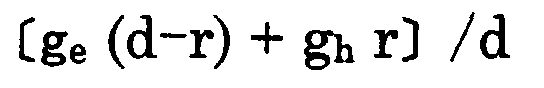
- equation (4) becomes equation (5).
- ⁇ i qgdS ( ⁇ h ⁇ h E)/d
- equation (8) In the conventional radiation detecting apparatus, by contrast, since g e and g h in the equations (2) and (3) are replaceable with Hecht's equations (6) and (7) below, equation (4) above becomes equation (8):
- Equation (9) shows that, in the conventional (non-injection type) radiation detecting apparatus, signals do not depend on electric field E, but depend on g or carriers generated.
- equation (5) for the first aspect of this invention shows that, in the first aspect of the invention, ⁇ i increases by ( ⁇ h ⁇ h E)/d times.
- a radiation detecting apparatus for converting incident radiation into electric signals, comprising:
- a positive bias voltage +V A is applied from the bias voltage supply Ve to one electrode side of a semiconductor layer 1B.
- the semiconductor layer 1B has a hole injection permitting structure 2B formed on a voltage application electrode side thereof, and an electron injection inhibiting structure 3B on a carrier collection electrode side.
- This apparatus has the same functions as the apparatus in the first aspect of the invention except that the direction for injecting holes h is reversed. Thus, the other details will not be discussed.
- a radiation detecting apparatus for converting incident radiation into electric signals, comprising:
- a radiation sensitive semiconductor layer 1C is formed of a p-type amorphous or polycrystal semiconductor of high specific resistance, with the ⁇ product of electrons e larger than the ⁇ product of holes h among the carriers generated.
- the electrons e which are the minority carriers in the semiconductor layer 1C contribute to the radiation detection.
- a negative bias voltage ⁇ V A is applied from the bias voltage supply Ve to one electrode side of semiconductor layer 1C.
- Electrons e are promptly injected from an electron injection permitting structure 2C formed on the electron application electrode side of semiconductor layer 1C, in a quantity corresponding to the quantity of the carriers generated by incident radiation.
- the semiconductor layer 1C has a hole injection inhibiting structure 3C formed on the voltage application electrode side thereof.
- This apparatus has the same functions as the apparatus in the first aspect of the invention in the other details. Thus, the other details will not be discussed.
- a radiation detecting apparatus for converting incident radiation into electric signals, comprising:
- a positive bias voltage +V A is applied from the bias voltage supply Ve to one electrode side of a semiconductor layer 1D.
- the semiconductor layer 1D has an electron injection permitting structure 3D formed on a carrier collection electrode side thereof, and a hole injection inhibiting structure 2D on a voltage application electrode side.
- This apparatus has the same functions as the apparatus in the third aspect of the invention except that the direction for injecting electrons e is reversed. Thus, the other details will not be discussed.
- the bias voltage applied to the voltage application electrode has a value within a range where an absolute value
- ⁇ i in equation (5) or (10) is larger than ⁇ i in equation (9), thereby reliably performing a radiation detecting operation with high sensitivity.
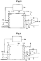
- Fig. 3 is a schematic view showing a basic construction of a principal portion of a radiation detecting apparatus in a first embodiment (embodiment according to the first aspect of this invention).
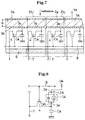
- Fig. 7 is a schematic sectional view showing a radiation sensor in the first embodiment.
- Fig. 8 is a basic electrical diagram of the radiation sensor in the first embodiment.
- Fig. 9 is a plan view showing a construction of the radiation sensor in the first embodiment.
- the radiation detecting apparatus in the first embodiment includes a radiation sensor having a radiation sensitive semiconductor layer 1A for generating carriers in response to incident radiation, a surface electrode (voltage application electrode) 2a disposed on a radiation incidence side of semiconductor layer 1A, carrier collection electrodes 3a arranged on a radiation non-incidence side (opposite from the radiation incidence side) of semiconductor layer 1A, charge storing capacitors Ca for storing charges generated by movement of the carriers in the semiconductor layer 1A, and thin film transistors (TFT) acting as switching elements 4, which are normally turned off (non-conductive), for taking out the charges stored in the capacitors Ca.
- TFT thin film transistors
- the apparatus in the first embodiment further includes a bias voltage supply (power source) Ve for applying a negative bias voltage ⁇ V A to the surface electrode 2a.
- the carriers generated by incident radiation and carriers injected, with the bias voltage applied to the surface electrode 2a move to the electrodes 3a, whereby charges accumulate in the capacitors Ca.
- the switching elements 4 are turned on (connected) whereby the charges are read and transmitted to charge-to-voltage converters (preamplifiers) 5 to be converted into radiation detection signals which are voltage signals.
- preamplifiers charge-to-voltage converters
- the semiconductor layer 1A is formed of an n-type amorphous semiconductor of high specific resistance with the ⁇ product of holes larger than the ⁇ product of electrons.
- This type of amorphous semiconductor includes, for example, non-dope amorphous selenium (a-Se) doped with no impurity, and alkali-dope amorphous selenium doped with an alkali metal such as Na.
- a-Se non-dope amorphous selenium
- alkali-dope amorphous selenium doped with an alkali metal such as Na alkali metal such as Na.
- the phrase "doped with no impurity" means that no impurity doping treatment is given deliberately.
- a desirable range of numerical values of high specific resistance is 10 9 ⁇ cm or more, and preferably 10 11 ⁇ cm or more.
- the amorphous semiconductor of course, is a semi-conductor material that realizes an enlarged detection area.
- a metal for the surface electrode 2a may, for example, be Au, Pt or the like which forms a Schottky junction with the n-type semiconductor.
- a metal for the carrier collection electrodes 3a may be ITO (indium tin oxide), Ti, Ni or the like which forms an ohmic junction with the n-type semiconductor. That is, in the first embodiment, a Schottky junction formed between the semiconductor layer 1A and surface electrode 2a constitutes an electron injection inhibiting structure 2A on the voltage application electrode side. Ohmic junctions formed between the semiconductor layer 1A and carrier collection electrodes 3a constitute a hole injection permitting structure 3A on the carrier collection electrode side.
- the amorphous semiconductor and the metals for forming the electrodes are not limited to the materials cited above.
- the radiation sensor of the apparatus in the first embodiment includes FET type thin film transistors acting as the switching elements 4 and the charge storing capacitors Ca, besides the semiconductor layer 1A and electrodes 2a and 3a, all formed on one insulating substrate 6.
- the capacitors Ca are in the form of SiO 2 layers or the like.
- the insulating substrate 6 is in the form of a glass substrate or the like.
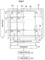
- the radiation sensor of the apparatus in the first embodiment is in the form of an area sensor (two-dimensional sensor) with numerous radiation detecting elements DU (e.g. 1024 ⁇ 1024) arranged along X- and Y-directions.
- Fig. 3 shows one detecting element DU as a basic construction.
- the surface electrode 2a is formed throughout as a common electrode for all the detecting elements DU.
- the carrier collection electrodes 3a are formed as individual electrodes for the respective detecting elements DU.
- the switching elements 4 and capacitors Ca also are formed one each for the respective detecting elements DU.
- the switching elements (thin film transistors) 4 of detecting elements DU have sources thereof connected to sense lines 7 arranged in the horizontal (X) direction, and gates connected to sense lines 8 arranged in the vertical (Y) direction.
- the sense lines 7 are connected to a multiplexer 10 through a group of charge-to-voltage converters (group of preamplifiers) 9.
- the sense lines 8 are connected to a gate driver 11.
- one charge-to-voltage converter 4 as shown in Fig. 3 is connected to each sense line 7.
- scan signals for fetching signals are inputted to the multiplexer 10 and gate driver 11.
- the detecting elements DU of the radiation sensor are identified by means of addresses (e.g. 0 to 1023) sequentially allocated to the detecting elements DU along the X- and Y-directions.
- the fetching scan signals serve as signals designating the addresses in the X-direction or Y-direction.
- the gate driver 11 applies a fetching voltage to the sense lines 8 arranged in the Y-direction. Then, detecting elements DU are selected on a column-by-column basis.
- the multiplexer 10 is switched by scan signals for the X-direction, the charges stored in the capacitors Ca of the detecting elements DU in the selected columns are successively outputted through the charge-to-voltage converter group 9 and multiplexer 10.
- the radiation detecting apparatus in the first embodiment is used as an X-ray detector of a fluoroscopic X-ray apparatus
- detection signals of the detecting elements DU are successively taken out of the multiplexer 10 as pixel signals.
- an image processor DT performs a necessary signal processing including a noise processing
- an image display MT displays a two-dimensional image (fluoroscopic image).
- the detection signal fetching mode of the radiation sensor in the first embodiment can be said broadly similar to that of ordinary imaging devices such as TV cameras.
- the radiation sensor may include an analog-to-digital converter (not shown), as necessary, in addition to the charge-to-voltage converter group 9, multiplexer 10 and gate driver 11, to promote an integrated construction.
- the charge-to-voltage converter group 9, multiplexer 10, gate driver 11 and the analog-to-digital converter may wholly or partly be installed separately.
- the thin film transistors for switching elements 4, capacitors Ca, carrier collection electrodes 3a, semiconductor layer 1A and surface electrode 2a are successively laminated on a surface of insulating substrate 6 by using the thin film forming technique based on one of various vacuum deposition methods or the pattern forming technique based on a photolithographic method.
- the bias voltage supply Ve is constructed to apply a voltage of minus (negative) polarity as the bias voltage to the surface electrode 2a, which voltage moves holes, among the carriers generated, from the radiation non-incident side toward the radiation incident side.
- the bias voltage supply Ve may be a fixed power supply for invariably outputting only a particular voltage, or may be a variable power supply for outputting voltages in a variable way.
- holes h which contribute to radiation detection are injected from the carrier collection electrodes 3a in a quantity corresponding to the carriers generated by incident radiation. This results in an increase in detection signals by ( ⁇ h ⁇ h E)/d times in proportion to the bias voltage, to achieve a significant improvement in detecting sensitivity.
- the holes h are minority carriers in the semiconductor layer 1A, and therefore little dark current occurs therein.
- the distance d between the electrodes i.e. thickness of semiconductor layer 1A
- the semiconductor layer 1A may be formed of a-Se
- the ⁇ product of holes may be 10 -6 cm 2 /V
- the ⁇ product of electrons may be 10 -7 cm 2 /V.
- each charge-to-voltage converter 5 for reading may be constructed switchable for connection to a plurality of capacitors Ca.
- the number of charge-to-voltage converters 5 may be reduced to realize a compact construction. That is, the radiation detecting apparatus according to this invention may be said suitable to the high sensitivity multi-channel type.
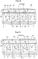
- FIG. 10 is a schematic sectional view showing a radiation sensor in the second embodiment.
- a radiation detecting apparatus in the second embodiment includes a p-type layer 1a of semiconductor film or organic film of low specific resistance formed between the surface electrode 2a and semiconductor layer 1A.
- a PN junction between the semiconductor layer 1A and p-type layer 1a constitutes the electron injection inhibiting structure 2A on the voltage application electrode side.
- the surface electrode 2a need not be formed of a material that provides a Schottky junction.
- the semiconductor film of low specific resistance for forming the p-type layer 1a may be Sb 2 Te 3 , Sb 2 S 3 or ZnTe, for example.
- the organic film may be polycarbonate or the like mixed with a hole transfer agent.
- FIG. 11 is a schematic sectional view showing a radiation sensor in the third embodiment.
- a radiation detecting apparatus in the third embodiment includes carrier selective injection layers 1b formed between the semiconductor layer 1A and carrier collection electrodes 3a.
- the carrier selective injection layers 1b are formed of a p-type semiconductor or organic film which tends to be injected with the holes having a large ⁇ product compared with the electron having a small ⁇ product.
- This p-type semiconductor may be, but is not limited to, Sb 2 S 3 , ZnTe or the like.
- the carrier selective injection layers 1b arranged under the semiconductor layer 1A constitute the hole injection permitting structure 3A.
- the carrier collection electrodes 3a need not necessarily form ohmic junctions, but may form Schottky junctions. This feature provides an additional advantage that the carrier collection electrodes 3 may be selected from a wide range of materials. The other details of the construction and function are the same as in the first embodiment described hereinbefore, and will not be described again.
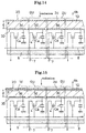
- FIG. 4 is a schematic view showing a basic construction of a principal portion of a radiation detecting apparatus in the fourth embodiment.
- Fig. 12 is a schematic sectional view showing a radiation sensor in the fourth embodiment.
- a positive bias voltage +V A is applied to the surface electrode 2b.
- the carrier collection electrodes 3b are formed of a metal such as ITO, Ti or Ni.
- p-type layers 1c of semiconductor film or organic film of low specific resistance are formed between a semiconductor layer 1B (e.g. non-dope amorphous selenium doped with no impurity or alkali-dope amorphous selenium doped with an alkali metal such as Na) and carrier collection electrodes 3b.
- the surface electrode 2b is formed of ITO, Ti, Ni or the like which forms an ohmic junction with an n-type semiconductor.
- the semiconductor film of low specific resistance for the p-type layer 1c may be Sb 2 Te 3 , Sb 2 S 3 or ZnTe, for example.
- the organic film may be polycarbonate or the like mixed with a hole transfer agent.
- PN junctions between the semiconductor layer 1B and p-type layers 1c constitute an electron injection inhibiting structure 3B on the carrier collection electrode side.
- An ohmic junction between the semiconductor layer 1B and surface electrode 2b provides a hole injection permitting structure 2B on the voltage application electrode side. Consequently, holes h are injected in the opposite direction to that in the first embodiment.
- the other details of the construction and function are the same as in the first embodiment described hereinbefore, and will not be described again.
- the carrier collection electrodes 3b may be formed of Au, Pt or the like which forms Schottky junctions with the n-type semiconductor, thereby allowing the p-type layers 1c to be omitted.
- the hole injection permitting structure 2B may be in the form of a p-type layer of semiconductor film or organic film of low specific resistance formed between the semiconductor layer 1B and surface electrode 2b.
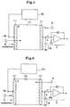
- FIG. 5 is a schematic view showing a basic construction of a principal portion of a radiation detecting apparatus in the fifth embodiment.
- Fig. 13 is a schematic sectional view showing a radiation sensor in the fifth embodiment.
- the radiation detecting apparatus in the fifth embodiment includes a radiation sensitive semiconductor layer 1C for generating carriers in response to incident radiation.
- the layer 1C is formed of a p-type polycrystal semiconductor of high specific resistance with the ⁇ product of electrons larger than the ⁇ product of holes.
- This polycrystal semiconductor which enables an enlarged detection area is not limited to a particular type, but may be a compound semiconductor such as CdZnTe, for example.
- a surface electrode 2c is formed of a metal such as Au or Pt which forms an ohmic junction with the p-type semiconductor.
- Carrier collection electrodes 3c are formed of a metal such as ITO or Ti which forms Schottky junctions with the p-type semiconductor.
- the polycrystal semiconductor and the metals for forming the electrodes are not limited to the materials cited above.
- the bias voltage supply Ve is constructed to apply a voltage of minus (negative) polarity as the bias voltage to the surface electrode 2c, which voltage moves electrons, among the carriers generated, from the radiation incident side toward the radiation non-incident side.
- the carriers contributing to radiation detection are electrons e.
- the ohmic junction formed between the semiconductor layer 1C and surface electrode 2c constitutes an electron injection permitting structure 2C on the voltage application electrode side.
- the Schottky junctions formed between the semiconductor layer 1C and carrier collection electrodes 3c constitute a hole injection inhibiting structure 3C on the carrier collection electrode side.
- the electrons e which contribute to radiation detection are injected from the surface electrode 2c in a quantity corresponding to the carriers generated by incident radiation. This results in an increase in detection signals by ( ⁇ e ⁇ e E)/d times in proportion to the bias voltage, to achieve a significant improvement in detecting sensitivity.
- the electrons e are minority carriers in the semiconductor layer 1C, and therefore little dark current occurs therein.
- the distance d between the electrodes i.e. thickness of semiconductor layer 1C
- the semiconductor layer 1C is formed of CdZnTe
- the ⁇ product of electrons may be 10- 5 cm 2 /V
- >90V results in ( ⁇ e ⁇ e E)/d>1 , to assure a radiation detection with high sensitivity.
- the electron injection permitting structure provided on the voltage application electrode side of semiconductor layer 1C may be in the form of an n-type layer of semiconductor film or organic film of low specific resistance formed between the semiconductor layer 1C and voltage application electrode (surface electrode 2C).
- the hole injection inhibiting structure provided on the carrier collection electrode side of semiconductor layer 1C may be in the form of n-type layers of semiconductor film or organic film of low specific resistance formed between the semiconductor layer 1C and carrier collection electrodes 3c.
- FIG. 6 is a schematic view showing a basic construction of a principal portion of a radiation detecting apparatus in the sixth embodiment.
- Fig. 14 is a schematic sectional view showing a radiation sensor in the sixth embodiment.
- a positive bias voltage +V A is applied to the surface electrode 2b.
- the surface electrode 2b and carrier collection electrodes 3b are both formed of a metal such as ITO, Ti or the like which forms Schottky junctions with a p-type semiconductor layer 1D.
- the p-type semiconductor layer 1D is similar to what is shown in the fifth embodiment, and is formed of a compound semiconductor such as CdZnTe, for example.
- the bias voltage is applied in the backward direction to the Schottky junction formed between the semiconductor layer 1D and surface electrode 2d, to provide a hole injection inhibiting structure 2D on the voltage application electrode side.
- the bias voltage is applied in the forward direction to the Schottky junctions formed between the semiconductor layer 1D and carrier collection electrodes 3d to provide an electron injection permitting structure 3D on the carrier collection electrode side.
- the electron injection permitting structure 3D may be in the form of n-type layers of semiconductor film or organic film of low specific resistance formed between the semiconductor layer 1D and carrier collection electrodes 3d.
- the carrier collection electrodes 3b may be formed of Au, Pt or the like which forms ohmic junctions with the p-type semiconductor.
- FIG. 15 is a schematic sectional view showing a radiation sensor in the seventh embodiment.
- a radiation detecting apparatus in the seventh embodiment includes an n-type layer 1d of semi-conductor film or organic film of low specific resistance formed between the surface electrode 2d and p-type semiconductor layer 1D.
- the p-type semiconductor layer 1D is similar to what is shown in the fifth and sixth embodiments.
- a bias voltage is applied in the backward direction to a PN junction between the semiconductor layer 1D and n-type layer 1d to provide a hole injection inhibiting structure 2D on the voltage application electrode side.
- the surface electrode 2d need not be formed of a material that provides a Schottky junction.
- the semiconductor film of low specific resistance for forming the n-type layer 1d may be CdS or CeO 2 , for example.
- the organic film may be polycarbonate or the like mixed with an electron transfer agent.
Abstract
Description
- This invention relates to radiation detecting apparatus of the direct conversion type used in the medical, industrial, nuclear and other fields, and more particularly to a technique of improving the sensitivity for detecting radiation.
- Radiation detecting apparatus employing semiconductor detectors include the indirect conversion type which first converts radiation (e.g. X rays) into light and then converts the light into electric signals by photoelectric conversion, and the direct conversion type which converts incident radiation directly into electric signals with a radiation sensitive semiconductor layer. The direct conversion type apparatus has electrodes formed on opposite surfaces of the radiation sensitive semiconductor layer. A predetermined voltage is applied to one of the electrodes (voltage application electrode). The other electrode (carrier collection electrode) collects carriers generated by incident radiation. The carriers are taken out as radiation detection signals, thereby enabling a detection of the radiation.
- A conventional radiation detecting apparatus of the direct conversion type employs a single crystal semiconductor as a material for the semiconductor layer. The single crystal semiconductor is used since it has excellent carrier transport characteristics compared with an amorphous or polycrystal semiconductor having numerous localized levels and grain boundaries. The conventional radiation detecting apparatus, with the excellent carrier transport characteristics of the single crystal semiconductor, is used as a radiation energy detector or a radiation pulse counter.
- Since only the carriers generated by incident radiation are taken out as signals, the conventional radiation detecting apparatus needs structures on both the opposite electrode sides for inhibiting carrier injection from the electrodes. Thus, the conventional apparatus has the following specific construction.
- As shown in Fig. 1, the conventional apparatus may include a single crystal semiconductor layer 51 of high specific resistance, which is doped with impurities to make one side p-type and the other side n-type. Structures 52 and 53 are formed on the opposite sides of semiconductor layer 51 to inhibit injection of electrons e and holes h, respectively. Alternatively, as shown in Fig. 2, the conventional apparatus may include an n-type (or p-type) single crystal semiconductor layer 61 of relatively low specific resistance, which may be doped with an impurity to make one side p-type (or n-type) or may have a structure 62 in the form of a barrier metal electrode on the one side to inhibit injection of electrons e (or holes h). The other side is guarded against injection of holes h (or electrons e) by the conductivity of the crystal per se. In Figs. 1 and 2, the left electrode acts as a bias voltage application electrode, and the right electrode as a carrier collection electrode.
- However, the conventional radiation detecting apparatus has a drawback that it can hardly meet a demand for an enlarged detecting area. In each of the medical, industrial, nuclear and other fields today, there is a strong demand for a semiconductor type radiation detecting apparatus with a large area and high sensitivity to realize a high-speed, highly sensitive and compact radiation detecting system. Under current conditions, a 3-inch diameter is the limit for radiation detecting, single crystal semiconductor materials. It is difficult to realize a semiconductor type radiation detecting apparatus with a large area and high sensitivity.
- With an amorphous or polycrystal semiconductor, on the other hand, 1000cm2 and larger sizes may be achieved by using a thin film making technique. However, sensitivity is insufficient because of the presence of localized levels and grain boundaries. Here again, it is difficult to realize a semiconductor type radiation detecting apparatus with a large area and high sensitivity.
- This invention has been made having regard to the state of the art noted above, and its object is to provide a semiconductor type radiation detecting apparatus with a large area and high sensitivity.
- The above object is fulfilled, according to a first aspect of this invention, by a radiation detecting apparatus for converting incident radiation into electric signals, comprising:
- a radiation sensitive semiconductor layer for generating carriers in form of electron-hole pairs in response to the incident radiation;
- a pair of electrodes formed on opposite surfaces of the semiconductor layer, respectively, one of the electrodes being a voltage application electrode to which a negative bias voltage is applied, the other electrode being a carrier collection electrode;
- a charge storing capacitor connected to the carrier collection electrode for storing charges generated by movement of the carriers in the semiconductor layer;
- a switching element connected to the capacitor, the switching element being turned off when the charges accumulate in the capacitor, and turned on when taking the charges out of the capacitor; and
- a charge-to-voltage converter means for converting the
charges taken out of the capacitor through the switching
element into voltage signals acting as radiation detection
signals;
wherein the semiconductor layer is formed of one of an n-type amorphous semiconductor and an n-type polycrystal semiconductor, both being of high specific resistance, with a µτ product of holes being larger than a µτ product of electrons, the µτ product being a product of mobility µ and mean life τ of the electrons and holes generated by the incident radiation; and
wherein the semiconductor layer has a structure formed on a voltage application electrode side thereof for inhibiting injection of electrons, and a structure formed on a carrier collection electrode side for permitting injection of holes. -
- The radiation detecting apparatus in the first aspect of the invention, as shown in Fig. 3, includes a radiation sensitive semiconductor layer 1A formed of an n-type amorphous or polycrystal semiconductor of high specific resistance, with the µτ product of holes h larger than the µτ product of electrons e among the carriers generated. When radiation is detected by this detecting apparatus, the holes h which are the minority carriers in the semiconductor layer 1A contribute to the radiation detection. A negative bias voltage ―VA is applied from a bias voltage supply Ve to one electrode side of semiconductor layer 1A. Consequently, holes h are promptly injected from a hole injection permitting structure 3A formed on the carrier collection electrode side of semiconductor layer 1A, in a quantity corresponding to the quantity of the carriers generated by the incident radiation. The semiconductor layer 1A has a high specific resistance, whereby the injection of holes h is not inhibited by the conductivity of the semiconductor layer 1A per se. On the other hand, an injection of electrons e is inhibited by an electron injection inhibiting structure 2A formed on the voltage application electrode side of semiconductor layer 1A.
- In the prior art, the injection of both holes h and electrons e is inhibited. The first aspect of the invention inhibits only the injection of electrons e which are the majority carriers not contributing to the improvement in sensitivity. Only the injection of holes h which contribute to the improvement in sensitivity is permitted to improve the sensitivity by a degree corresponding to the increase in the holes h. The holes h injected are the minority carriers in the semiconductor layer 1A, and thus an increase in dark current is suppressed. Of course, the detection area may be enlarged since the semiconductor layer 1A is formed of an amorphous or polycrystal semiconductor material.
- Charges generated by movement of holes h accumulate in a charge storing capacitor Ca while a switching element 4 is turned off. When the switching element 4 is turned on, the charges stored are read from a charge-to-voltage converter 5 as voltage signals acting as radiation detection signals. Thus, a detecting operation is not interrupted, with holes h accumulating in the capacitor Ca, even during a non-signal reading period, which provides an advantage in terms of sensitivity. Further, in the case of a multichannel construction, the charge-to-voltage converter 5 for reading detection signals may be arranged switchable for connection to a plurality of capacitors, thereby reducing the number of charge-to-voltage converters 5 required.
- Next, the detecting sensitivity of the radiation detecting apparatus in the first aspect of the invention will be described in terms of quantity.
- Current i flowing when an electric field E is applied and radiation (X rays) is emitted to a semiconductor layer 1 having a sectional area S and a thickness corresponding to a distance d between the electrodes, is expressed by
- On the other hand, where the quantity of carriers generated per unit volume and unit time is g (cm-3 sec-1), since irradiation is assumed to be steady (
- Since
- Further, since the injection of electrons e is inhibited here, equation (4) becomes equation (5).
- In this case, since µe τe « µh τh, the value of Δi hardly changes.
- In the conventional radiation detecting apparatus, by contrast, since ge and gh in the equations (2) and (3) are replaceable with Hecht's equations (6) and (7) below, equation (4) above becomes equation (8):


- Further, the expression in { } of equation (8) approachesas E increases. This value is equal to g, and therefore equation (8) finally becomes equation (9).
- Equation (9) shows that, in the conventional (non-injection type) radiation detecting apparatus, signals do not depend on electric field E, but depend on g or carriers generated.
- A comparison between equation (5) for the first aspect of this invention and equation (9) for the prior art shows that, in the first aspect of the invention, Δi increases by (µh τh E)/d times. The rate of increase is proportional to electric field E, and electric field
- In a second aspect of the invention, there is provided a radiation detecting apparatus for converting incident radiation into electric signals, comprising:
- a radiation sensitive semiconductor layer for generating carriers in form of electron-hole pairs in response to the incident radiation;
- a pair of electrodes formed on opposite surfaces of the semiconductor layer, respectively, one of the electrodes being a voltage application electrode to which a positive bias voltage is applied, the other electrode being a carrier collection electrode;
- a charge storing capacitor connected to the carrier collection electrode for storing charges generated by movement of the carriers in the semiconductor layer;
- a switching element connected to the capacitor, the switching element being turned off when the charges accumulate in the capacitor, and turned on when taking the charges out of the capacitor; and
- a charge-to-voltage converter for converting the charges
taken out of the capacitor through the switching element into
voltage signals acting as radiation detection signals;
wherein the semiconductor layer is formed of one of an n-type amorphous semiconductor and an n-type polycrystal semiconductor, both being of high specific resistance, with a µτ product of holes being larger than a µτ product of electrons, the µτ product being a product of mobility µ and mean life τ of the electrons and holes generated by the incident radiation; and
wherein the semiconductor layer has a structure formed on a voltage application electrode side thereof for permitting injection of holes, and a structure formed on a carrier collection electrode side for inhibiting injection of electrons. -
- With the radiation detecting apparatus in the second aspect of the invention, as shown in Fig. 4, a positive bias voltage +VA is applied from the bias voltage supply Ve to one electrode side of a semiconductor layer 1B. The semiconductor layer 1B has a hole injection permitting structure 2B formed on a voltage application electrode side thereof, and an electron injection inhibiting structure 3B on a carrier collection electrode side. This apparatus has the same functions as the apparatus in the first aspect of the invention except that the direction for injecting holes h is reversed. Thus, the other details will not be discussed.
- In a third aspect of the invention, there is provided a radiation detecting apparatus for converting incident radiation into electric signals, comprising:
- a radiation sensitive semiconductor layer for generating carriers in form of electron-hole pairs in response to the incident radiation;
- a pair of electrodes formed on opposite surfaces of the semiconductor layer, respectively, one of the electrodes being a voltage application electrode to which a negative bias voltage is applied, the other electrode being a carrier collection electrode;
- a charge storing capacitor connected to the carrier collection electrode for storing charges generated by movement of the carriers in the semiconductor layer;
- a switching element connected to the capacitor, the switching element being turned off when the charges accumulate in the capacitor, and turned on when taking the charges out of the capacitor; and
- a charge-to-voltage converter for converting the charges
taken out of the capacitor through the switching element into
voltage signals acting as radiation detection signals;
wherein the semiconductor layer is formed of one of a p-type amorphous semiconductor and a p-type polycrystal semiconductor, both being of high specific resistance, with a µτ product of electrons being larger than a µτ product of holes, the µτ product being a product of mobility µ and mean life τ of the electrons and holes generated by the incident radiation; and
wherein the semiconductor layer has a structure formed on a voltage application electrode side thereof for permitting injection of electrons, and a structure formed on a carrier collection electrode side for inhibiting injection of holes. -
- With the radiation detecting apparatus in the third aspect of the invention, as shown in Fig. 5, a radiation sensitive semiconductor layer 1C is formed of a p-type amorphous or polycrystal semiconductor of high specific resistance, with the µτ product of electrons e larger than the µτ product of holes h among the carriers generated. The electrons e which are the minority carriers in the semiconductor layer 1C contribute to the radiation detection. A negative bias voltage ―VA is applied from the bias voltage supply Ve to one electrode side of semiconductor layer 1C. Electrons e are promptly injected from an electron injection permitting structure 2C formed on the electron application electrode side of semiconductor layer 1C, in a quantity corresponding to the quantity of the carriers generated by incident radiation. On the other hand, the semiconductor layer 1C has a hole injection inhibiting structure 3C formed on the voltage application electrode side thereof. Thus, holes h are not injected, but only electrons e are injected.
- Since the injection of holes h is inhibited here, the fore-going equation (5) becomes equation (10) below:
- Since µh τh « µe τe, the value of Δi, of course, hardly changes. Sensitivity is improved since Δi increases by (µe τe E)/d times.
- This apparatus has the same functions as the apparatus in the first aspect of the invention in the other details. Thus, the other details will not be discussed.
- In a fourth aspect of the invention, there is provided a radiation detecting apparatus for converting incident radiation into electric signals, comprising:
- a radiation sensitive semiconductor layer for generating carriers in form of electron-hole pairs in response to the incident radiation;
- a pair of electrodes formed on opposite surfaces of the semiconductor layer, respectively, one of the electrodes being a voltage application electrode to which a positive bias voltage is applied, the other electrode being a carrier collection electrode;
- a charge storing capacitor connected to the carrier collection electrode for storing charges generated by movement of the carriers in the semiconductor layer;
- a switching element connected to the capacitor, the switching element being turned off when the charges accumulate in the capacitor, and turned on when taking the charges out of the capacitor; and
- a charge-to-voltage converter for converting the charges
taken out of the capacitor through the switching element into
voltage signals acting as radiation detection signals;
wherein the semiconductor layer is formed of one of a p-type amorphous semiconductor and a p-type polycrystal semiconductor, both being of high specific resistance, with a µτ product of electrons being larger than a µτ product of holes, the µτ product being a product of mobility µ and mean life τ of the electrons and holes generated by the incident radiation; and
wherein the semiconductor layer has a structure formed on a voltage application electrode side thereof for inhibiting injection of holes, and a structure formed on a carrier collection electrode side for permitting injection of electrons. -
- With the radiation detecting apparatus in the fourth aspect of the invention, as shown in Fig. 6, a positive bias voltage +VA is applied from the bias voltage supply Ve to one electrode side of a semiconductor layer 1D. The semiconductor layer 1D has an electron injection permitting structure 3D formed on a carrier collection electrode side thereof, and a hole injection inhibiting structure 2D on a voltage application electrode side. This apparatus has the same functions as the apparatus in the third aspect of the invention except that the direction for injecting electrons e is reversed. Thus, the other details will not be discussed.
- In the radiation detecting apparatus in the first to fourth aspects of the invention, preferably, the bias voltage applied to the voltage application electrode has a value within a range where an absolute value | VA | of the bias voltage is
- With the bias voltage set as above, Δi in equation (5) or (10) is larger than Δi in equation (9), thereby reliably performing a radiation detecting operation with high sensitivity.
- For the purpose of illustrating the invention, there are shown in the drawings several forms which are presently preferred, it being understood, however, that the invention is not limited to the precise arrangement and instrumentalities shown.
- Fig. 1 is a schematic view showing a basic construction of a principal portion of a conventional radiation detecting apparatus;
- Fig. 2 is a schematic view showing a basic construction of a principal portion of another conventional radiation detecting apparatus;
- Fig. 3 is a schematic view showing a basic construction of a principal portion of a radiation detecting apparatus according to the first aspect of this invention;
- Fig. 4 is a schematic view showing a basic construction of a principal portion of a radiation detecting apparatus according to the second aspect of this invention;
- Fig. 5 is a schematic view showing a basic construction of a principal portion of a radiation detecting apparatus according to the third aspect of this invention;
- Fig. 6 is a schematic view showing a basic construction of a principal portion of a radiation detecting apparatus according to the fourth aspect of this invention;
- Fig. 7 is a schematic sectional view showing a radiation sensor in a first embodiment;
- Fig. 8 is a basic electrical diagram of the radiation sensor in the first embodiment;
- Fig. 9 is a plan view showing a construction of the radiation sensor in the first embodiment;
- Fig. 10 is a schematic sectional view showing a radiation sensor in a second embodiment;
- Fig. 11 is a schematic sectional view showing a radiation sensor in a third embodiment;
- Fig. 12 is a schematic sectional view showing a radiation sensor in a fourth embodiment;
- Fig. 13 is a schematic sectional view showing a radiation sensor in a fifth embodiment;
- Fig. 14 is a schematic sectional view showing a radiation sensor in a sixth embodiment; and
- Fig. 15 is a schematic sectional view showing a radiation sensor in a seventh embodiment.
-
- Preferred embodiments of the present invention will be described in detail hereinafter with reference to the drawings.
- Fig. 3 is a schematic view showing a basic construction of a principal portion of a radiation detecting apparatus in a first embodiment (embodiment according to the first aspect of this invention). Fig. 7 is a schematic sectional view showing a radiation sensor in the first embodiment. Fig. 8 is a basic electrical diagram of the radiation sensor in the first embodiment. Fig. 9 is a plan view showing a construction of the radiation sensor in the first embodiment.
- As shown in Figs. 3 and 7, the radiation detecting apparatus in the first embodiment includes a radiation sensor having a radiation sensitive semiconductor layer 1A for generating carriers in response to incident radiation, a surface electrode (voltage application electrode) 2a disposed on a radiation incidence side of semiconductor layer 1A, carrier collection electrodes 3a arranged on a radiation non-incidence side (opposite from the radiation incidence side) of semiconductor layer 1A, charge storing capacitors Ca for storing charges generated by movement of the carriers in the semiconductor layer 1A, and thin film transistors (TFT) acting as switching elements 4, which are normally turned off (non-conductive), for taking out the charges stored in the capacitors Ca. The apparatus in the first embodiment further includes a bias voltage supply (power source) Ve for applying a negative bias voltage ―VA to the surface electrode 2a. The carriers generated by incident radiation and carriers injected, with the bias voltage applied to the surface electrode 2a, move to the electrodes 3a, whereby charges accumulate in the capacitors Ca. In time of reading, the switching elements 4 are turned on (connected) whereby the charges are read and transmitted to charge-to-voltage converters (preamplifiers) 5 to be converted into radiation detection signals which are voltage signals. Each component will particularly be described hereinafter.
- In the apparatus in the first embodiment, the semiconductor layer 1A is formed of an n-type amorphous semiconductor of high specific resistance with the µτ product of holes larger than the µτ product of electrons. This type of amorphous semiconductor includes, for example, non-dope amorphous selenium (a-Se) doped with no impurity, and alkali-dope amorphous selenium doped with an alkali metal such as Na. As used herein, the phrase "doped with no impurity" means that no impurity doping treatment is given deliberately. A desirable range of numerical values of high specific resistance is 109 Ω cm or more, and preferably 1011 Ω cm or more. The amorphous semiconductor, of course, is a semi-conductor material that realizes an enlarged detection area.
- A metal for the surface electrode 2a may, for example, be Au, Pt or the like which forms a Schottky junction with the n-type semiconductor. A metal for the carrier collection electrodes 3a may be ITO (indium tin oxide), Ti, Ni or the like which forms an ohmic junction with the n-type semiconductor. That is, in the first embodiment, a Schottky junction formed between the semiconductor layer 1A and surface electrode 2a constitutes an electron injection inhibiting structure 2A on the voltage application electrode side. Ohmic junctions formed between the semiconductor layer 1A and carrier collection electrodes 3a constitute a hole injection permitting structure 3A on the carrier collection electrode side. Of course, the amorphous semiconductor and the metals for forming the electrodes are not limited to the materials cited above.
- As shown in Figs. 7 and 9, the radiation sensor of the apparatus in the first embodiment includes FET type thin film transistors acting as the switching elements 4 and the charge storing capacitors Ca, besides the semiconductor layer 1A and electrodes 2a and 3a, all formed on one insulating substrate 6. The capacitors Ca are in the form of SiO2 layers or the like. The insulating substrate 6 is in the form of a glass substrate or the like.
- Further, the radiation sensor of the apparatus in the first embodiment is in the form of an area sensor (two-dimensional sensor) with numerous radiation detecting elements DU (e.g. 1024 × 1024) arranged along X- and Y-directions. Fig. 3 shows one detecting element DU as a basic construction. As shown in Figs. 7 and 9, the surface electrode 2a is formed throughout as a common electrode for all the detecting elements DU. The carrier collection electrodes 3a are formed as individual electrodes for the respective detecting elements DU. The switching elements 4 and capacitors Ca also are formed one each for the respective detecting elements DU.
- In the radiation sensor in the first embodiment, as shown in Fig. 9, the switching elements (thin film transistors) 4 of detecting elements DU have sources thereof connected to sense lines 7 arranged in the horizontal (X) direction, and gates connected to sense lines 8 arranged in the vertical (Y) direction. The sense lines 7 are connected to a multiplexer 10 through a group of charge-to-voltage converters (group of preamplifiers) 9. The sense lines 8 are connected to a gate driver 11. In the charge-to-voltage converter group 9, one charge-to-voltage converter 4 as shown in Fig. 3 is connected to each sense line 7.
- In the radiation sensor in the first embodiment, scan signals for fetching signals are inputted to the multiplexer 10 and gate driver 11. The detecting elements DU of the radiation sensor are identified by means of addresses (e.g. 0 to 1023) sequentially allocated to the detecting elements DU along the X- and Y-directions. Thus, the fetching scan signals serve as signals designating the addresses in the X-direction or Y-direction.
- In response to scan signals for the Y-direction, the gate driver 11 applies a fetching voltage to the sense lines 8 arranged in the Y-direction. Then, detecting elements DU are selected on a column-by-column basis. When, the multiplexer 10 is switched by scan signals for the X-direction, the charges stored in the capacitors Ca of the detecting elements DU in the selected columns are successively outputted through the charge-to-voltage converter group 9 and multiplexer 10.
- Where the radiation detecting apparatus in the first embodiment is used as an X-ray detector of a fluoroscopic X-ray apparatus, for example, detection signals of the detecting elements DU are successively taken out of the multiplexer 10 as pixel signals. Then, as shown in chain lines in Fig. 9, an image processor DT performs a necessary signal processing including a noise processing, and an image display MT displays a two-dimensional image (fluoroscopic image).
- Thus, the detection signal fetching mode of the radiation sensor in the first embodiment can be said broadly similar to that of ordinary imaging devices such as TV cameras.
- In the first embodiment, the radiation sensor may include an analog-to-digital converter (not shown), as necessary, in addition to the charge-to-voltage converter group 9, multiplexer 10 and gate driver 11, to promote an integrated construction. However, the charge-to-voltage converter group 9, multiplexer 10, gate driver 11 and the analog-to-digital converter may wholly or partly be installed separately.
- In fabricating the radiation sensor in the first embodiment, the thin film transistors for switching elements 4, capacitors Ca, carrier collection electrodes 3a, semiconductor layer 1A and surface electrode 2a are successively laminated on a surface of insulating substrate 6 by using the thin film forming technique based on one of various vacuum deposition methods or the pattern forming technique based on a photolithographic method.
- On the other hand, the bias voltage supply Ve is constructed to apply a voltage of minus (negative) polarity as the bias voltage to the surface electrode 2a, which voltage moves holes, among the carriers generated, from the radiation non-incident side toward the radiation incident side. The bias voltage supply Ve may be a fixed power supply for invariably outputting only a particular voltage, or may be a variable power supply for outputting voltages in a variable way.
- In this case, holes h which contribute to radiation detection are injected from the carrier collection electrodes 3a in a quantity corresponding to the carriers generated by incident radiation. This results in an increase in detection signals by (µh τh E)/d times in proportion to the bias voltage, to achieve a significant improvement in detecting sensitivity. The holes h are minority carriers in the semiconductor layer 1A, and therefore little dark current occurs therein.
- In the radiation detecting apparatus in the first embodiment, the distance d between the electrodes (i.e. thickness of semiconductor layer 1A) may be 0.07cm, the semiconductor layer 1A may be formed of a-Se, the µτ product of holes may be 10-6cm2/V, and the µτ product of electrons may be 10-7cm2/V. Then, a bias voltage in a range of | ―VA | >4900V results in
- Further, in the apparatus in the first embodiment, a detecting operation continues, without interruption, with holes h accumulating in the capacitors Ca even outside a signal reading period. This is advantageous in terms of sensitivity. In a multi-channel construction as in the first embodiment, each charge-to-voltage converter 5 for reading may be constructed switchable for connection to a plurality of capacitors Ca. Thus, the number of charge-to-voltage converters 5 may be reduced to realize a compact construction. That is, the radiation detecting apparatus according to this invention may be said suitable to the high sensitivity multi-channel type.
- A second embodiment (another embodiment according to the first aspect of the invention) will be described next. Fig. 10 is a schematic sectional view showing a radiation sensor in the second embodiment.
- As shown in Fig. 10, a radiation detecting apparatus in the second embodiment includes a p-type layer 1a of semiconductor film or organic film of low specific resistance formed between the surface electrode 2a and semiconductor layer 1A. A PN junction between the semiconductor layer 1A and p-type layer 1a constitutes the electron injection inhibiting structure 2A on the voltage application electrode side. Thus, the surface electrode 2a need not be formed of a material that provides a Schottky junction, The semiconductor film of low specific resistance for forming the p-type layer 1a may be Sb2Te3, Sb2S3 or ZnTe, for example. The organic film may be polycarbonate or the like mixed with a hole transfer agent.
- The other details of the construction and function are the same as in the first embodiment described hereinbefore, and will not be described again.
- A third embodiment (further embodiment according to the first aspect of the invention) will be described next. Fig. 11 is a schematic sectional view showing a radiation sensor in the third embodiment.
- As shown in Fig. 11, a radiation detecting apparatus in the third embodiment includes carrier selective injection layers 1b formed between the semiconductor layer 1A and carrier collection electrodes 3a. In the apparatus in the third embodiment, the carrier selective injection layers 1b are formed of a p-type semiconductor or organic film which tends to be injected with the holes having a large µτ product compared with the electron having a small µτ product. This p-type semiconductor may be, but is not limited to, Sb2S3, ZnTe or the like.
- In the apparatus in the third embodiment, the carrier selective injection layers 1b arranged under the semiconductor layer 1A constitute the hole injection permitting structure 3A. Thus, the carrier collection electrodes 3a need not necessarily form ohmic junctions, but may form Schottky junctions. This feature provides an additional advantage that the carrier collection electrodes 3 may be selected from a wide range of materials. The other details of the construction and function are the same as in the first embodiment described hereinbefore, and will not be described again.
- A fourth embodiment (embodiment according to the second aspect of the invention) will be described next. Fig. 4 is a schematic view showing a basic construction of a principal portion of a radiation detecting apparatus in the fourth embodiment. Fig. 12 is a schematic sectional view showing a radiation sensor in the fourth embodiment.
- In the radiation detecting apparatus in the fourth embodiment, as shown in Fig. 12, a positive bias voltage +VA is applied to the surface electrode 2b. The carrier collection electrodes 3b are formed of a metal such as ITO, Ti or Ni. Further, p-type layers 1c of semiconductor film or organic film of low specific resistance are formed between a semiconductor layer 1B (e.g. non-dope amorphous selenium doped with no impurity or alkali-dope amorphous selenium doped with an alkali metal such as Na) and carrier collection electrodes 3b. The surface electrode 2b is formed of ITO, Ti, Ni or the like which forms an ohmic junction with an n-type semiconductor. The semiconductor film of low specific resistance for the p-type layer 1c may be Sb2Te3, Sb2S3 or ZnTe, for example. The organic film may be polycarbonate or the like mixed with a hole transfer agent. Thus, PN junctions between the semiconductor layer 1B and p-type layers 1c constitute an electron injection inhibiting structure 3B on the carrier collection electrode side. An ohmic junction between the semiconductor layer 1B and surface electrode 2b provides a hole injection permitting structure 2B on the voltage application electrode side. Consequently, holes h are injected in the opposite direction to that in the first embodiment. The other details of the construction and function are the same as in the first embodiment described hereinbefore, and will not be described again.
- In the fourth embodiment, the carrier collection electrodes 3b may be formed of Au, Pt or the like which forms Schottky junctions with the n-type semiconductor, thereby allowing the p-type layers 1c to be omitted. However, this usually is undesirable since, in the case of a heavy metal such as Au or Pt, metal atoms could infiltrate into the thin film transistor forming the switching elements 4 below, thereby to degrade its property. The hole injection permitting structure 2B may be in the form of a p-type layer of semiconductor film or organic film of low specific resistance formed between the semiconductor layer 1B and surface electrode 2b.
- A fifth embodiment (embodiment according to the third aspect of the invention) will be described next. Fig. 5 is a schematic view showing a basic construction of a principal portion of a radiation detecting apparatus in the fifth embodiment. Fig. 13 is a schematic sectional view showing a radiation sensor in the fifth embodiment.
- As shown in Figs. 5 and 13, the radiation detecting apparatus in the fifth embodiment includes a radiation sensitive semiconductor layer 1C for generating carriers in response to incident radiation. The layer 1C is formed of a p-type polycrystal semiconductor of high specific resistance with the µτ product of electrons larger than the µτ product of holes. This polycrystal semiconductor which enables an enlarged detection area is not limited to a particular type, but may be a compound semiconductor such as CdZnTe, for example. A surface electrode 2c is formed of a metal such as Au or Pt which forms an ohmic junction with the p-type semiconductor. Carrier collection electrodes 3c are formed of a metal such as ITO or Ti which forms Schottky junctions with the p-type semiconductor. Of course, the polycrystal semiconductor and the metals for forming the electrodes are not limited to the materials cited above.
- On the other hand, the bias voltage supply Ve is constructed to apply a voltage of minus (negative) polarity as the bias voltage to the surface electrode 2c, which voltage moves electrons, among the carriers generated, from the radiation incident side toward the radiation non-incident side.
- Thus, in the apparatus in the fifth embodiment, the carriers contributing to radiation detection are electrons e. The ohmic junction formed between the semiconductor layer 1C and surface electrode 2c constitutes an electron injection permitting structure 2C on the voltage application electrode side. The Schottky junctions formed between the semiconductor layer 1C and carrier collection electrodes 3c constitute a hole injection inhibiting structure 3C on the carrier collection electrode side.
- In this case, electrons e which contribute to radiation detection are injected from the surface electrode 2c in a quantity corresponding to the carriers generated by incident radiation. This results in an increase in detection signals by (µe τe E)/d times in proportion to the bias voltage, to achieve a significant improvement in detecting sensitivity. The electrons e are minority carriers in the semiconductor layer 1C, and therefore little dark current occurs therein. In the radiation detecting apparatus in the fifth embodiment, the distance d between the electrodes (i.e. thickness of semiconductor layer 1C) is 0.03cm, the semiconductor layer 1C is formed of CdZnTe, the µτ product of electrons may be 10-5cm2/V, and the µτ product of holes may be 10-6cm2/V. Then, a bias voltage of | ―VA | >90V results in
- In this embodiment, the electron injection permitting structure provided on the voltage application electrode side of semiconductor layer 1C may be in the form of an n-type layer of semiconductor film or organic film of low specific resistance formed between the semiconductor layer 1C and voltage application electrode (surface electrode 2C).
- The hole injection inhibiting structure provided on the carrier collection electrode side of semiconductor layer 1C may be in the form of n-type layers of semiconductor film or organic film of low specific resistance formed between the semiconductor layer 1C and carrier collection electrodes 3c.
- The other details of the construction and function are the same as in the first embodiment described hereinbefore, and will not be described again.
- A sixth embodiment (embodiment according to the fourth aspect of the invention) will be described next. Fig. 6 is a schematic view showing a basic construction of a principal portion of a radiation detecting apparatus in the sixth embodiment. Fig. 14 is a schematic sectional view showing a radiation sensor in the sixth embodiment.
- In the radiation detecting apparatus in the sixth embodiment, as shown in Figs. 6 and 14, a positive bias voltage +VA is applied to the surface electrode 2b. The surface electrode 2b and carrier collection electrodes 3b are both formed of a metal such as ITO, Ti or the like which forms Schottky junctions with a p-type semiconductor layer 1D. The p-type semiconductor layer 1D is similar to what is shown in the fifth embodiment, and is formed of a compound semiconductor such as CdZnTe, for example.
- In the sixth embodiment, the bias voltage is applied in the backward direction to the Schottky junction formed between the semiconductor layer 1D and surface electrode 2d, to provide a hole injection inhibiting structure 2D on the voltage application electrode side. The bias voltage is applied in the forward direction to the Schottky junctions formed between the semiconductor layer 1D and carrier collection electrodes 3d to provide an electron injection permitting structure 3D on the carrier collection electrode side.
- The electron injection permitting structure 3D may be in the form of n-type layers of semiconductor film or organic film of low specific resistance formed between the semiconductor layer 1D and carrier collection electrodes 3d.
- In the sixth embodiment, the carrier collection electrodes 3b may be formed of Au, Pt or the like which forms ohmic junctions with the p-type semiconductor. However, this usually is undesirable since, in the case of a heavy metal such as Au or Pt, metal atoms could infiltrate into the thin film transistor forming the switching elements 4 below, thereby to degrade its property.
- The other details of the construction and function are the same as in the first embodiment described hereinbefore, and will not be described again.
- A seventh embodiment (another embodiment according to the fourth aspect of the invention) will be described next. Fig. 15 is a schematic sectional view showing a radiation sensor in the seventh embodiment.
- As shown in Fig. 15, a radiation detecting apparatus in the seventh embodiment includes an n-type layer 1d of semi-conductor film or organic film of low specific resistance formed between the surface electrode 2d and p-type semiconductor layer 1D. The p-type semiconductor layer 1D is similar to what is shown in the fifth and sixth embodiments. A bias voltage is applied in the backward direction to a PN junction between the semiconductor layer 1D and n-type layer 1d to provide a hole injection inhibiting structure 2D on the voltage application electrode side. The surface electrode 2d need not be formed of a material that provides a Schottky junction. The semiconductor film of low specific resistance for forming the n-type layer 1d may be CdS or CeO2, for example. The organic film may be polycarbonate or the like mixed with an electron transfer agent. The other details of the construction and function are the same as in the first embodiment described hereinbefore, and will not be described again.
- This invention is not limited to the foregoing embodiments, but may be modified as follows:
- (1) In the fifth to seventh embodiments, the compound semiconductor is CdZnTe. However, CdTe and PbI2 may also be used as the compound semiconductor. It is also possible to use halogen-dope amorphous selenium doped with a halogen such as Cl.
- (2) In the described embodiments, the surface electrode and carrier collection electrodes are formed of metal. Instead, n-type semiconductors such as CdS and CeO2 and p-type semiconductors such as Sb2Te3 and Sb2S3 may be used where appropriate.
- (3) The radiation detecting apparatus in the first to fourth embodiments each include an area sensor with numerous detecting elements DU arranged in matrix form. This construction may be modified to include a line sensor with a plurality of detecting elements DU arranged vertically or horizontally in a single column or row, or to include only one detecting element DU.
- (4) The radiation detected by the radiation detecting apparatus according to this invention is not limited to X rays. The apparatus is intended for all types of radiation.
-
- The present invention may be embodied in other specific forms without departing from the spirit or essential attributes thereof and, accordingly, reference should be made to the appended claims, rather than to the foregoing specification, as indicating the scope of the invention.
Claims (33)
- A radiation detecting apparatus for converting incident radiation into electric signals, comprising:a radiation sensitive semiconductor layer for generating carriers in form of electron-hole pairs in response to the incident radiation;a pair of electrodes formed on opposite surfaces of said semiconductor layer, respectively, one of said electrodes being a voltage application electrode to which a negative bias voltage is applied, the other electrode being a carrier collection electrode;a charge storing capacitor connected to said carrier collection electrode for storing charges generated by movement of the carriers in said semiconductor layer;a switching element connected to said capacitor, said switching element being turned off when the charges accumulate in said capacitor, and turned on when taking the charges out of said capacitor; andcharge-to-voltage converting means for converting the charges taken out of said capacitor through said switching element into voltage signals acting as radiation detection signals;
wherein said semiconductor layer is formed of one of an n-type amorphous semiconductor and an n-type polycrystal semiconductor, both being of high specific resistance, with a µτ product of holes being larger than a µτ product of electrons, the µτ product being a product of mobility µ and mean life τ of the electrons and holes generated by the incident radiation; and
wherein said semiconductor layer has a structure formed on a voltage application electrode side thereof for inhibiting injection of electrons, and a structure formed on a carrier collection electrode side for permitting injection of holes. - A radiation detecting apparatus as defined in claim 1, wherein the bias voltage applied to said voltage application electrode has a value within a range where an absolute value | VA | of the bias voltage is
- A radiation detecting apparatus as defined in claim 1, wherein said semiconductor layer is formed of one of non-dope amorphous selenium doped with no impurity, and alkali-dope amorphous selenium doped with an alkali metal.
- A radiation detecting apparatus as defined in claim 1, wherein said structure for inhibiting injection of electrons comprises a Schottky junction formed between said semiconductor layer and said voltage application electrode.
- A radiation detecting apparatus as defined in claim 1, wherein said structure for inhibiting injection of electrons comprises a p-type layer of one of a semiconductor film and an organic film, both being of low specific resistance, formed between said semiconductor layer and said voltage application electrode.
- A radiation detecting apparatus as defined in claim 1, wherein said structure for permitting injection of holes comprises an ohmic junction formed between said semiconductor layer and said carrier collection electrode.
- A radiation detecting apparatus as defined in claim 1, wherein said structure for permitting injection of holes comprises a carrier selective injection layer of one of a p-type semiconductor film and a p-type organic film which tend to inject holes rather than electrons, formed between said semiconductor layer and said carrier collection electrode.
- A radiation detecting apparatus as defined in claim 1, wherein said apparatus includes a plurality of detecting elements in a two-dimensional arrangement, each having at least said semiconductor layer, said voltage application electrode, said carrier collection electrode, said charge storing capacitor and said switching element.
- A radiation detecting apparatus for converting incident radiation into electric signals, comprising:a radiation sensitive semiconductor layer for generating carriers in form of electron-hole pairs in response to the incident radiation;a pair of electrodes formed on opposite surfaces of said semiconductor layer, respectively, one of said electrodes being a voltage application electrode to which a positive bias voltage is applied, the other electrode being a carrier collection electrode;a charge storing capacitor connected to said carrier collection electrode for storing charges generated by movement of the carriers in said semiconductor layer;a switching element connected to said capacitor, said switching element being turned off when the charges accumulate in said capacitor, and turned on when taking the charges out of said capacitor; andcharge-to-voltage converting means for converting the charges taken out of said capacitor through said switching element into voltage signals acting as radiation detection signals;
wherein said semiconductor layer is formed of one of an n-type amorphous semiconductor and an n-type polycrystal semiconductor, both being of high specific resistance, with a µτ product of holes being larger than a µτ product of electrons, the µτ product being a product of mobility µ and mean life τ of the electrons and holes generated by the incident radiation; and
wherein said semiconductor layer has a structure formed on a voltage application electrode side thereof for permitting injection of holes, and a structure formed on a carrier collection electrode side for inhibiting injection of electrons. - A radiation detecting apparatus as defined in claim 9, wherein the bias voltage applied to said voltage application electrode has a value within a range where an absolute value | VA | of the bias voltage is
- A radiation detecting apparatus as defined in claim 9, wherein said semiconductor layer is formed of one of non-dope amorphous selenium doped with no impurity, and alkali-dope amorphous selenium doped with an alkali metal.
- A radiation detecting apparatus as defined in claim 9, wherein said structure for permitting injection of holes comprises an ohmic junction formed between said semiconductor layer and said voltage application electrode.
- A radiation detecting apparatus as defined in claim 9, wherein said structure for permitting injection of holes comprises a p-type layer of one of semiconductor film and organic film, both being of low specific resistance, formed between said semiconductor layer and said voltage application electrode.
- A radiation detecting apparatus as defined in claim 9, wherein said structure for inhibiting injection of electrons comprises a p-type layer of one of a semiconductor film and an organic film, both being of low specific resistance, formed between said semiconductor layer and said carrier collection electrode.
- A radiation detecting apparatus as defined in claim 9, wherein said apparatus includes a plurality of detecting elements in a two-dimensional arrangement, each having at least said semiconductor layer, said voltage application electrode, said carrier collection electrode, said charge storing capacitor and said switching element.
- A radiation detecting apparatus for converting incident radiation into electric signals, comprising:a radiation sensitive semiconductor layer for generating carriers in form of electron-hole pairs in response to the incident radiation;a pair of electrodes formed on opposite surfaces of said semiconductor layer, respectively, one of said electrodes being a voltage application electrode to which a negative bias voltage is applied, the other electrode being a carrier collection electrode;a charge storing capacitor connected to said carrier collection electrode for storing charges generated by movement of the carriers in said semiconductor layer;a switching element connected to said capacitor, said switching element being turned off when the charges accumulate in said capacitor, and turned on when taking the charges out of said capacitor; andcharge-to-voltage converting means for converting the charges taken out of said capacitor through said switching element into voltage signals acting as radiation detection signals;
wherein said semiconductor layer is formed of one of a p-type amorphous semiconductor and a p-type polycrystal semiconductor, both being of high specific resistance, with a µτ product of electrons being larger than a µτ product of holes, the µτ product being a product of mobility µ and mean life τ of the electrons and holes generated by the incident radiation; and
wherein said semiconductor layer has a structure formed on a voltage application electrode side thereof for permitting injection of electrons, and a structure formed on a carrier collection electrode side for inhibiting injection of holes. - A radiation detecting apparatus as defined in claim 16, wherein the bias voltage applied to said voltage application electrode has a value within a range where an absolute value | VA | of the bias voltage is
- A radiation detecting apparatus as defined in claim 16, wherein said semiconductor layer comprises a compound semiconductor selected from the group consisting of CdZnTe, CdTe and PbI2.
- A radiation detecting apparatus as defined in claim 16, wherein said semiconductor layer comprises a halogen-dope amorphous selenium doped with a halogen.
- A radiation detecting apparatus as defined in claim 16, wherein said structure for permitting injection of electrons comprises an ohmic junction formed between said semiconductor layer and said voltage application electrode.
- A radiation detecting apparatus as defined in claim 16, wherein said structure for permitting injection of electrons comprises an n-type layer of one of a semiconductor film and an organic film, both being of low specific resistance, formed between said semiconductor layer and said voltage application electrode.
- A radiation detecting apparatus as defined in claim 16, wherein said structure for inhibiting injection of holes comprises a Schottky junction formed between said semiconductor layer and said carrier collection electrode.
- A radiation detecting apparatus as defined in claim 16, wherein said structure for inhibiting injection of holes comprises an n-type layer of one of a semiconductor film and an organic film, both being of low specific resistance, formed between said semiconductor layer and said carrier collection electrode.
- A radiation detecting apparatus as defined in claim 16,
wherein said apparatus includes a plurality of detecting elements in a two-dimensional arrangement, each having at least said semiconductor layer, said voltage application electrode, said carrier collection electrode, said charge storing capacitor and said switching element. - A radiation detecting apparatus for converting incident radiation into electric signals, comprising:a radiation sensitive semiconductor layer for generating carriers in form of electron-hole pairs in response to the incident radiation;a pair of electrodes formed on opposite surfaces of said semiconductor layer, respectively, one of said electrodes being a voltage application electrode to which a positive bias voltage is applied, the other electrode being a carrier collection electrode;a charge storing capacitor connected to said carrier collection electrode for storing charges generated by movement of the carriers in said semiconductor layer;a switching element connected to said capacitor, said switching element being turned off when the charges accumulate in said capacitor, and turned on when taking the charges out of said capacitor; andcharge-to-voltage converting means for converting the charges taken out of said capacitor through said switching element into voltage signals acting as radiation detection signals;
wherein said semiconductor layer is formed of one of a p-type amorphous semiconductor and a p-type polycrystal semiconductor, both being of high specific resistance, with a µτ product of electrons being larger than a µτ product of holes, the µτ product being a product of mobility µ and mean life τ of the electrons and holes generated by the incident radiation; and
wherein said semiconductor layer has a structure formed on a voltage application electrode side thereof for inhibiting injection of holes, and a structure formed on a carrier collection electrode side for permitting injection of electrons. - A radiation detecting apparatus as defined in claim 25, wherein the bias voltage applied to said voltage application electrode has a value within a range where an absolute value | VA | of the bias voltage is
- A radiation detecting apparatus as defined in claim 25, wherein said semiconductor layer comprises a compound semiconductor selected from the group consisting of CdZnTe, CdTe and PbI2.
- A radiation detecting apparatus as defined in claim 25, wherein said semiconductor layer comprises a halogen-dope amorphous selenium doped with a halogen.
- A radiation detecting apparatus as defined in claim 25, wherein said structure for inhibiting injection of holes comprises a Schottky junction formed between said semiconductor layer and said voltage application electrode.
- A radiation detecting apparatus as defined in claim 25, wherein said structure for inhibiting injection of holes comprises an n-type layer of one of a semiconductor film and an organic film, both being of low specific resistance, formed between said semiconductor layer and said voltage application electrode.
- A radiation detecting apparatus as defined in claim 25, wherein said structure for permitting injection of electrons comprises a Schottky junction formed between said semiconductor layer and said carrier collection electrode.
- A radiation detecting apparatus as defined in claim 25, wherein said structure for permitting injection of electrons comprises an n-type layer of one of a semiconductor film and an organic film, both being of low specific resistance, formed between said semiconductor layer and said carrier collection electrode.
- A radiation detecting apparatus as defined in claim 25, wherein said apparatus includes a plurality of detecting elements in a two-dimensional arrangement, each having at least said semiconductor layer, said voltage application electrode, said carrier collection electrode, said charge storing capacitor and said switching element.
Applications Claiming Priority (4)
| Application Number | Priority Date | Filing Date | Title |
|---|---|---|---|
| JP35130998 | 1998-12-10 | ||
| JP35130998 | 1998-12-10 | ||
| JP10252899 | 1999-04-09 | ||
| JP10252899A JP4059463B2 (en) | 1998-12-10 | 1999-04-09 | Radiation detector |
Publications (3)
| Publication Number | Publication Date |
|---|---|
| EP1009038A2 true EP1009038A2 (en) | 2000-06-14 |
| EP1009038A3 EP1009038A3 (en) | 2000-07-12 |
| EP1009038B1 EP1009038B1 (en) | 2005-11-16 |
Family
ID=26443244
Family Applications (1)
| Application Number | Title | Priority Date | Filing Date |
|---|---|---|---|
| EP99124549A Expired - Lifetime EP1009038B1 (en) | 1998-12-10 | 1999-12-09 | Radiation detecting apparatus |
Country Status (5)
| Country | Link |
|---|---|
| US (1) | US6528794B1 (en) |
| EP (1) | EP1009038B1 (en) |
| JP (1) | JP4059463B2 (en) |
| CN (1) | CN1187840C (en) |
| DE (1) | DE69928361T2 (en) |
Cited By (6)
| Publication number | Priority date | Publication date | Assignee | Title |
|---|---|---|---|---|
| EP1079437A2 (en) * | 1999-08-26 | 2001-02-28 | Shimadzu Corporation | Radiation detecting apparatus |
| EP1139429A2 (en) * | 2000-03-29 | 2001-10-04 | Shindengen Electric Manufacturing Company, Limited | X-ray detection plate and x-ray detector |
| US6635860B2 (en) * | 2001-04-12 | 2003-10-21 | Shimadzu Corporation | Radiation detector |
| US7233003B2 (en) * | 2003-09-24 | 2007-06-19 | Shimadzu Corporation | Radiation detector |
| JP2008151795A (en) * | 2007-12-25 | 2008-07-03 | Shimadzu Corp | X-ray detector |
| US7554092B2 (en) * | 2002-04-23 | 2009-06-30 | Shimadzu Corporation | X-ray detector |
Families Citing this family (16)
| Publication number | Priority date | Publication date | Assignee | Title |
|---|---|---|---|---|
| AU4603200A (en) * | 1999-04-26 | 2000-11-10 | Simage Oy | Device for imaging radiation |
| JP2003004857A (en) * | 2001-06-25 | 2003-01-08 | Canon Inc | Radiation detector and radiation photographing system using the same |
| CN102151612A (en) * | 2002-06-21 | 2011-08-17 | 德塞拉股份有限公司 | An electrostatic fluid accelerator for and method of controlling a fluid flow |
| JP2004138472A (en) * | 2002-10-17 | 2004-05-13 | Mitsubishi Heavy Ind Ltd | Radiation detecting element, radiation detector, radiation ct device, and radiation inspection device |
| US7884438B2 (en) * | 2005-07-29 | 2011-02-08 | Varian Medical Systems, Inc. | Megavoltage imaging with a photoconductor based sensor |
| DE102007007140B4 (en) * | 2007-02-09 | 2009-01-29 | Astrium Gmbh | Method and arrangement for detecting mechanical defects of a semiconductor device, in particular a solar cell or solar cell arrangement |
| KR101354791B1 (en) | 2009-10-05 | 2014-01-22 | 가부시키가이샤 시마쓰세사쿠쇼 | Radiation detector |
| US8304272B2 (en) | 2010-07-02 | 2012-11-06 | International Business Machines Corporation | Germanium photodetector |
| US8545689B2 (en) | 2010-09-02 | 2013-10-01 | International Business Machines Corporation | Gallium electrodeposition processes and chemistries |
| US20120055612A1 (en) | 2010-09-02 | 2012-03-08 | International Business Machines Corporation | Electrodeposition methods of gallium and gallium alloy films and related photovoltaic structures |
| WO2012081109A1 (en) * | 2010-12-16 | 2012-06-21 | 株式会社リガク | Strip detector |
| DE102011089776B4 (en) * | 2011-12-23 | 2015-04-09 | Siemens Aktiengesellschaft | Detector element, radiation detector, medical device and method for producing such a detector element |
| CN102709395B (en) * | 2012-06-12 | 2014-12-31 | 上海大学 | Preparation method of CdZnTe thin-film ultraviolet light detector |
| US9207335B2 (en) * | 2013-04-29 | 2015-12-08 | Westinghouse Electric Company Llc | Self powered neutron detector |
| JP6544440B2 (en) * | 2015-11-19 | 2019-07-17 | 株式会社島津製作所 | Semiconductor detector |
| US10910432B1 (en) * | 2019-07-23 | 2021-02-02 | Cyber Medical Imaging, Inc. | Use of surface patterning for fabricating a single die direct capture dental X-ray imaging sensor |
Citations (4)
| Publication number | Priority date | Publication date | Assignee | Title |
|---|---|---|---|---|
| US4233514A (en) * | 1978-12-14 | 1980-11-11 | General Electric Company | Solid state radiation detector and arrays thereof |
| JPH01302775A (en) * | 1988-05-31 | 1989-12-06 | Toshiba Corp | Radiation detecting element |
| US5396072A (en) * | 1992-08-17 | 1995-03-07 | U. S. Philips Corporation | X-ray image detector |
| WO1996003773A1 (en) * | 1994-07-27 | 1996-02-08 | Litton Systems Canada Limited | Radiation imaging panel |
Family Cites Families (10)
| Publication number | Priority date | Publication date | Assignee | Title |
|---|---|---|---|---|
| US3077386A (en) * | 1958-01-02 | 1963-02-12 | Xerox Corp | Process for treating selenium |
| US3640812A (en) * | 1970-09-02 | 1972-02-08 | Rca Corp | Method of making electrical contacts on the surface of a semiconductor device |
| US4127860A (en) * | 1977-04-18 | 1978-11-28 | Rca Corporation | Integrated circuit mesa bipolar device on insulating substrate incorporating Schottky barrier contact |
| US5335219A (en) * | 1991-01-18 | 1994-08-02 | Ovshinsky Stanford R | Homogeneous composition of microcrystalline semiconductor material, semiconductor devices and directly overwritable memory elements fabricated therefrom, and arrays fabricated from the memory elements |
| JPH08509550A (en) * | 1993-04-28 | 1996-10-08 | ユニバーシティ オブ サリー | Radiation detector |
| US5892227A (en) * | 1994-09-29 | 1999-04-06 | Yissum Research Development Company Of The Hebrew University Of Jerusalem | Radiation detection system and processes for preparing the same |
| US5677538A (en) * | 1995-07-07 | 1997-10-14 | Trustees Of Boston University | Photodetectors using III-V nitrides |
| WO1997010616A1 (en) * | 1995-09-12 | 1997-03-20 | Philips Electronics N.V. | X-ray image sensor |
| US5677539A (en) * | 1995-10-13 | 1997-10-14 | Digirad | Semiconductor radiation detector with enhanced charge collection |
| IL119478A (en) * | 1996-10-23 | 2000-08-13 | Israel Atomic Energy Comm | Method and system for obtaining x-ray single photon spectroscopic data using room-temperature solid state detectors by measuring the induced electron current |
-
1999
- 1999-04-09 JP JP10252899A patent/JP4059463B2/en not_active Expired - Lifetime
- 1999-12-06 US US09/455,508 patent/US6528794B1/en not_active Expired - Lifetime
- 1999-12-07 CN CNB991254147A patent/CN1187840C/en not_active Expired - Fee Related
- 1999-12-09 DE DE69928361T patent/DE69928361T2/en not_active Expired - Lifetime
- 1999-12-09 EP EP99124549A patent/EP1009038B1/en not_active Expired - Lifetime
Patent Citations (4)
| Publication number | Priority date | Publication date | Assignee | Title |
|---|---|---|---|---|
| US4233514A (en) * | 1978-12-14 | 1980-11-11 | General Electric Company | Solid state radiation detector and arrays thereof |
| JPH01302775A (en) * | 1988-05-31 | 1989-12-06 | Toshiba Corp | Radiation detecting element |
| US5396072A (en) * | 1992-08-17 | 1995-03-07 | U. S. Philips Corporation | X-ray image detector |
| WO1996003773A1 (en) * | 1994-07-27 | 1996-02-08 | Litton Systems Canada Limited | Radiation imaging panel |
Non-Patent Citations (1)
| Title |
|---|
| PATENT ABSTRACTS OF JAPAN vol. 014, no. 099 (E-0893), 22 February 1990 (1990-02-22) & JP 01 302775 A (TOSHIBA CORP), 6 December 1989 (1989-12-06) * |
Cited By (8)
| Publication number | Priority date | Publication date | Assignee | Title |
|---|---|---|---|---|
| EP1079437A2 (en) * | 1999-08-26 | 2001-02-28 | Shimadzu Corporation | Radiation detecting apparatus |
| EP1079437A3 (en) * | 1999-08-26 | 2004-08-18 | Shimadzu Corporation | Radiation detecting apparatus |
| EP1139429A2 (en) * | 2000-03-29 | 2001-10-04 | Shindengen Electric Manufacturing Company, Limited | X-ray detection plate and x-ray detector |
| EP1139429A3 (en) * | 2000-03-29 | 2005-10-26 | Shindengen Electric Manufacturing Company, Limited | X-ray detection plate and x-ray detector |
| US6635860B2 (en) * | 2001-04-12 | 2003-10-21 | Shimadzu Corporation | Radiation detector |
| US7554092B2 (en) * | 2002-04-23 | 2009-06-30 | Shimadzu Corporation | X-ray detector |
| US7233003B2 (en) * | 2003-09-24 | 2007-06-19 | Shimadzu Corporation | Radiation detector |
| JP2008151795A (en) * | 2007-12-25 | 2008-07-03 | Shimadzu Corp | X-ray detector |
Also Published As
| Publication number | Publication date |
|---|---|
| DE69928361T2 (en) | 2006-08-10 |
| EP1009038B1 (en) | 2005-11-16 |
| JP4059463B2 (en) | 2008-03-12 |
| EP1009038A3 (en) | 2000-07-12 |
| JP2000230981A (en) | 2000-08-22 |
| DE69928361D1 (en) | 2005-12-22 |
| CN1187840C (en) | 2005-02-02 |
| US6528794B1 (en) | 2003-03-04 |
| CN1257312A (en) | 2000-06-21 |
Similar Documents
| Publication | Publication Date | Title |
|---|---|---|
| EP1009038B1 (en) | Radiation detecting apparatus | |
| EP2919269B1 (en) | Photosensor arrays for detection of radiation and process for the preparation thereof | |
| EP1711968B1 (en) | Phototransistor | |
| EP0791230B1 (en) | X-ray image sensor | |
| JP3440031B2 (en) | Direct conversion digital X-ray or gamma ray detector | |
| US7884438B2 (en) | Megavoltage imaging with a photoconductor based sensor | |
| WO2001061729A1 (en) | Fully depleted back illuminated ccd | |
| US20190115377A1 (en) | Imaging sensor | |
| US6495817B1 (en) | Radiation detecting apparatus having an electrodeless region | |
| CA2482279C (en) | Radiation detector | |
| US6489618B1 (en) | Radiation image pickup device | |
| CA2455319C (en) | Active-matrix substrate and electromagnetic wave detector | |
| US6252215B1 (en) | Hybrid sensor pixel architecture with gate line and drive line synchronization | |
| US6005238A (en) | Hybrid sensor pixel architecture with linearization circuit | |
| US6031248A (en) | Hybrid sensor pixel architecture | |
| KR100642655B1 (en) | Radiation detecting apparatus | |
| US20030155517A1 (en) | Radiation detecting element, radiation image pickup apparatus and radiation detecting method | |
| US20050056829A1 (en) | Reducing dark current of photoconductor using heterojunction that maintains high x-ray sensitivity | |
| US6051827A (en) | Hybrid sensor pixel architecture with threshold response | |
| US6969896B1 (en) | Photodetector biasing scheme | |
| JP2003240859A (en) | Radiation detecting device and radiation imaging unit | |
| JP2001108748A (en) | Radiographic image picking-up device | |
| JPH11103089A (en) | Multiplication type photoelectric conversion device and multiplication type solid-state image sensing device using the same |
Legal Events
| Date | Code | Title | Description |
|---|---|---|---|
| PUAI | Public reference made under article 153(3) epc to a published international application that has entered the european phase |
Free format text: ORIGINAL CODE: 0009012 |
|
| PUAL | Search report despatched |
Free format text: ORIGINAL CODE: 0009013 |
|
| AK | Designated contracting states |
Kind code of ref document: A2 Designated state(s): DE FR GB |
|
| AX | Request for extension of the european patent |
Free format text: AL;LT;LV;MK;RO;SI |
|
| AK | Designated contracting states |
Kind code of ref document: A3 Designated state(s): AT BE CH CY DE DK ES FI FR GB GR IE IT LI LU MC NL PT SE |
|
| AX | Request for extension of the european patent |
Free format text: AL;LT;LV;MK;RO;SI |
|
| 17P | Request for examination filed |
Effective date: 20000907 |
|
| AKX | Designation fees paid |
Free format text: DE FR GB |
|
| 17Q | First examination report despatched |
Effective date: 20040609 |
|
| GRAP | Despatch of communication of intention to grant a patent |
Free format text: ORIGINAL CODE: EPIDOSNIGR1 |
|
| GRAS | Grant fee paid |
Free format text: ORIGINAL CODE: EPIDOSNIGR3 |
|
| GRAA | (expected) grant |
Free format text: ORIGINAL CODE: 0009210 |
|
| AK | Designated contracting states |
Kind code of ref document: B1 Designated state(s): DE FR GB |
|
| REG | Reference to a national code |
Ref country code: GB Ref legal event code: FG4D |
|
| REF | Corresponds to: |
Ref document number: 69928361 Country of ref document: DE Date of ref document: 20051222 Kind code of ref document: P |
|
| ET | Fr: translation filed | ||
| PLBE | No opposition filed within time limit |
Free format text: ORIGINAL CODE: 0009261 |
|
| STAA | Information on the status of an ep patent application or granted ep patent |
Free format text: STATUS: NO OPPOSITION FILED WITHIN TIME LIMIT |
|
| 26N | No opposition filed |
Effective date: 20060817 |
|
| REG | Reference to a national code |
Ref country code: DE Ref legal event code: R082 Ref document number: 69928361 Country of ref document: DE Representative=s name: KILIAN KILIAN & PARTNER MBB PATENTANWAELTE, DE Ref country code: DE Ref legal event code: R082 Ref document number: 69928361 Country of ref document: DE Representative=s name: KILIAN KILIAN & PARTNER, DE |
|
| REG | Reference to a national code |
Ref country code: FR Ref legal event code: PLFP Year of fee payment: 17 |
|
| PGFP | Annual fee paid to national office [announced via postgrant information from national office to epo] |
Ref country code: GB Payment date: 20151209 Year of fee payment: 17 Ref country code: DE Payment date: 20151201 Year of fee payment: 17 |
|
| PGFP | Annual fee paid to national office [announced via postgrant information from national office to epo] |
Ref country code: FR Payment date: 20151110 Year of fee payment: 17 |
|
| REG | Reference to a national code |
Ref country code: DE Ref legal event code: R119 Ref document number: 69928361 Country of ref document: DE |
|
| GBPC | Gb: european patent ceased through non-payment of renewal fee |
Effective date: 20161209 |
|
| REG | Reference to a national code |
Ref country code: FR Ref legal event code: ST Effective date: 20170831 |
|
| PG25 | Lapsed in a contracting state [announced via postgrant information from national office to epo] |
Ref country code: FR Free format text: LAPSE BECAUSE OF NON-PAYMENT OF DUE FEES Effective date: 20170102 |
|
| PG25 | Lapsed in a contracting state [announced via postgrant information from national office to epo] |
Ref country code: DE Free format text: LAPSE BECAUSE OF NON-PAYMENT OF DUE FEES Effective date: 20170701 Ref country code: GB Free format text: LAPSE BECAUSE OF NON-PAYMENT OF DUE FEES Effective date: 20161209 |