EP1111804A2 - Schnelle Hadamard-Transformationsvorrichtung für CDMA-Übertragungssysteme - Google Patents
Schnelle Hadamard-Transformationsvorrichtung für CDMA-Übertragungssysteme Download PDFInfo
- Publication number
- EP1111804A2 EP1111804A2 EP20000128244 EP00128244A EP1111804A2 EP 1111804 A2 EP1111804 A2 EP 1111804A2 EP 20000128244 EP20000128244 EP 20000128244 EP 00128244 A EP00128244 A EP 00128244A EP 1111804 A2 EP1111804 A2 EP 1111804A2
- Authority
- EP
- European Patent Office
- Prior art keywords
- input
- shift register
- output
- latch
- hadamard transform
- Prior art date
- Legal status (The legal status is an assumption and is not a legal conclusion. Google has not performed a legal analysis and makes no representation as to the accuracy of the status listed.)
- Withdrawn
Links
- 238000004891 communication Methods 0.000 title description 4
- 239000013598 vector Substances 0.000 description 10
- 238000010586 diagram Methods 0.000 description 7
- 238000000034 method Methods 0.000 description 6
- 238000010295 mobile communication Methods 0.000 description 5
- 238000013139 quantization Methods 0.000 description 3
- 239000011159 matrix material Substances 0.000 description 2
- 238000001228 spectrum Methods 0.000 description 2
- 102100034033 Alpha-adducin Human genes 0.000 description 1
- 101000799076 Homo sapiens Alpha-adducin Proteins 0.000 description 1
- 101000629598 Rattus norvegicus Sterol regulatory element-binding protein 1 Proteins 0.000 description 1
- 238000004364 calculation method Methods 0.000 description 1
- 238000005314 correlation function Methods 0.000 description 1
- 238000005516 engineering process Methods 0.000 description 1
- 230000010354 integration Effects 0.000 description 1
- 238000004519 manufacturing process Methods 0.000 description 1
- 230000007704 transition Effects 0.000 description 1
Images


Classifications
-
- H—ELECTRICITY
- H04—ELECTRIC COMMUNICATION TECHNIQUE
- H04B—TRANSMISSION
- H04B1/00—Details of transmission systems, not covered by a single one of groups H04B3/00 - H04B13/00; Details of transmission systems not characterised by the medium used for transmission
- H04B1/69—Spread spectrum techniques
- H04B1/707—Spread spectrum techniques using direct sequence modulation
- H04B1/709—Correlator structure
- H04B1/7093—Matched filter type
-
- H—ELECTRICITY
- H03—ELECTRONIC CIRCUITRY
- H03M—CODING; DECODING; CODE CONVERSION IN GENERAL
- H03M7/00—Conversion of a code where information is represented by a given sequence or number of digits to a code where the same, similar or subset of information is represented by a different sequence or number of digits
-
- H—ELECTRICITY
- H04—ELECTRIC COMMUNICATION TECHNIQUE
- H04B—TRANSMISSION
- H04B1/00—Details of transmission systems, not covered by a single one of groups H04B3/00 - H04B13/00; Details of transmission systems not characterised by the medium used for transmission
- H04B1/69—Spread spectrum techniques
- H04B1/707—Spread spectrum techniques using direct sequence modulation
- H04B1/709—Correlator structure
- H04B1/7093—Matched filter type
- H04B2001/70935—Matched filter type using a bank of matched fileters, e.g. Fast Hadamard Transform
Definitions
- the invention relates to a fast hadamard transform device and, in particular, to the transform device which is adapted to perform quadrature modulation of spread signals in a CDMA (Code Division Multiple Access) mobile communication system.
- CDMA Code Division Multiple Access
- CDMA which is focused as the next generation standard mobile communication method
- mobile communication terminals in the system can simultaneously communicate among a plurality of channels by using the same frequency band.
- a spread spectrum communication method is used in the CDMA mobile communication system.
- the spread spectrum communication method can be realized, for example, by a Walsh quadrature modulation technique which uses a Walsh code such that a correlation function becomes zero at every channel.
- the Walsh code can be expressed by a Hadamard transform matrix which is composed of elements of "+1" and "-1".
- high speed or fast processing based on a butterfly computation can be achieved by carrying out Hadamard transform using the Hadamard transform matrix.
- a device which enables such high speed or fast Hadamard transform based on the butterfly computation may be called a fast Hadamard transform (FHT) device.
- FHT fast Hadamard transform
- a conventional fast Hadamard transform device performs both addition and subtraction in the butterfly computation. Specifically, the addition is performed by using n/2 of (p - 1 + log 2 n) bits adders while the subtraction is performed by using n/2 of (p - 1 + log 2 n) bits subtractors.
- the number of quantization bits is represented by p and an n-th order Hadamard transform is carried out in the following. Especially, the description will be mainly made about an eighth-order fast Hadamard transform.
- the conventional fast Hadamard transform device if the number of bits used for calculation is increased to k times, the device has to be enlarged in size to 3k times. This is because three latches, that is, an input latch, a latch with selector, and an output latch should be prepared for each bit in the conventional fast Hadamard transform.
- each of adders and subtractors should process the number of bits equal to (p - 1 + log 2 n)
- each of latches should include a bit number of register stages which is equal to (p - 1 + log 2 n) .
- an object of the invention to provide a fast Hadamard transform device which can be configured in a small scale and developed in a short time, that is, within short developing TAT (Turn Around Time), even if the number of bits to be processed is increased.
- a fast Hadamard transform device which transforms n elements of input data each of which is composed of p bits.
- the device comprises n of shift register units each of which inputs the corresponding element of the input data at the predetermined input timing and outputs the bits in the input data serially, and n/2 of butterfly computation units each of which receives a bit from each two of the n shift register units and performs addition and subtraction on the two bits to supply each operation result to a determined shift register unit.
- each of the shift register units operates as output latches holding (p + log 2 n) signals from one of the butterfly computation units at the predetermined output timing, and operates as (p + log 2 n) steps of shift registers in response to entering the input data and signals from one of the butterfly computation units at the other timing.
- each of the butterfly computation units includes an adder which performs addition on two bits which are shifted from the different shift register units and a carry bit which is stored in the former addition, a subtractor which performs subtraction on two bits which are shifted from the different shift register units and a borrow bit which is stored in the former subtraction.
- a fast Hadamard transform device of the third aspect of the invention and in the device, each of the carry bit and the borrow bit is stored in a delay circuit which is initialized every (log 2 n * (p + log 2 n)) shift timings.
- a fast Hadamard transform device of the fourth aspect of the invention serial output of the shift register unit corresponding to the 2q-1-th (1 ⁇ q ⁇ 4, q is a natural number) order is connected to an input to the adder of the q-th butterfly computation unit, serial output of the shift register unit corresponding to the 2q-th order is connected to an input to the subtractor of the q-th butterfly computation unit, an output from the adder of the r-th (1 ⁇ r ⁇ 4, r is a natural number) butterfly computation unit is connected to the serial input of the r-th shift register unit, and an output from the subtractor of the r-th butterfly computation unit is connected to the serial input of the r+4-th shift register unit.
- the conventional fast Hadamard transform device can carry out the n-th order of the Hadamard transform.
- the illustrated device carries out an eighth order of the Hadamard transform, that is, n is equal to eight and the number of quantization bits is equal to p.
- the device receives eight elements (or dimension) of input vector X in a bit serial manner and each of the elements x 1 - x 8 of the vector X is successively latched by each of a first input latch 10 1 through an eighth input latch 10 8 in the illustrated manner.
- Each of output terminals of the first input latch 10 1 through the eighth input latch 10 8 can be put into a high impedance state in response to an input latch output enable signal (not shown). Both the output terminals of the first input latch 10 1 and the second latch 10 2 are connected to an adder 11 1 and a subtractor 12 1 .
- adders and subtractors concerned with the conventional fast Hadamard transform device can carry out addition and subtraction in response to the (p - 1 + log 2 n) of bits, and therefore each of the adders may be denoted as (p-1 + log 2 n) adder and each of the subtractors may be denoted as (p - 1 + log 2 n) subtractor.
- both the output terminals of the third input latch 10 3 and the fourth latch 10 4 are connected to an adder 11 2 and a subtractor 12 2 .
- Both the output terminals of the fifth input latch 10 5 and the sixth latch 10 6 are connected to an adder 11 3 and a subtractor 12 3 .
- Both the output terminals of the seventh input latch 10 7 and the eighth latch 10 8 are connected to an adder 11 4 and a subtractor 12 4 .
- An output terminal of the adder 11 1 is connected to a first output latch 13 1 and a first latch 14 1 with no selector.
- An output terminal of the subtractor 12 1 is connected to a fifth output latch 13 5 and a first latch 15 1 with selector.
- An output terminal of the adder 11 2 is connected to a second output latch 13 2 and a second latch 15 2 with selector.
- An output terminal of the subtractor 12 2 is connected to a sixth output latch 13 6 and a third latch 15 3 with selector.
- An output terminal of the adder 11 3 is connected to a third output latch 13 3 and a fourth latch 15 4 with selector.
- An output terminal of the subtractor 12 3 is connected to a seventh output latch 13 7 and a fifth latch 15 5 with selector.
- An output terminal of the adder 11 4 is connected to a fourth output latch 13 4 and a sixth latch 15 6 with selector.
- An output terminal of the subtractor 12 4 is connected to an eighth output latch 13 8 and a second latch 14 2 with no selector.
- a butterfly computation unit is configured by a pair of an adder and a subtractor (such as the adder 11 1 and the subtractor 12 1 ), both of which are given the same inputs.
- the first latch 14 1 with no selector and the second latch 14 2 with no selector latch an output of an adder or a subtractor in response to a selector latch signal (not shown). Also, an output terminal of the first latch 14 1 with no selector and an output terminal of the second latch 14 2 with no selector are connected to an output terminal of the first input latch 10 1 and an output terminal of the eighth input latch 10 8 , respectively. Both of them are kept at high impedance states in response to entire latch output enable signals (not shown) which are delivered to all of the latches with and without selectors, as will become clear later.
- the first latch with selector 15 1 through the sixth latch with selector 15 6 latch an output of an adder or a subtractor in response to a selector latch signal (not shown).
- Each of the first latch 15 1 with selector through the sixth latch 15 6 with selector has two output terminals A and B, and outputs latched data from one of the terminals according to a "latch with selector" switch signal (not shown).
- the "latch with selector" switch signal serves to selectively switch only the firth through the sixth latches with selector, with the first and the second latches 141 and 142 kept intact, and therefore will be referred to as a selective switch signal.
- these terminals are connected to one of output terminals of the second input latch 10 2 through the seventh input latch 10 7 and are kept at high impedance states by the above-mentioned entire latch output enable signal.
- the first output latch 13 1 through the eighth output latch 13 8 latch output of the corresponding adder or the corresponding subtractor in according to an output latch signal (not shown) and outputs elements y 1 - y 8 of the output vector Y.
- each of the first input latch 10 1 through the eighth input latch 10 8 latches each of the corresponding elements ((a) in Fig. 2) of the eight elements of the input vector X by an input latch clock ((b) in Fig. 2).
- the input-latch output enable signal is turned to a low level signal "L” ((c) in Fig. 2) and the entire latch output enable signal is turned to a high level signal "H” ((e) in Fig. 2) and is sent to all of the latches 14 1 , 14 2 , 15 1 to 15 6 to put them into the high impedance states.
- latch signals which are latched in all the input latches are supplied to the adders 11 1 - 11 4 or the subtractors 12 1 - 12 4 , with all of the latches 14 1 , 14 2 , 15 1 to 15 6 kept in the high impedance states.
- output terminals A of the first through the sixth latches 15 1 - 15 6 with selectors are selected by the selective switch signal ((d) in Fig. 2).
- the feedback signal w 1 (t 1 ) is stored to the first latch 14 1 with no selector and w 8 (t 1 ) is stored to the second latch 14 2 with no selector in response to a selector latch signal ((f) in Fig. 2).
- the remaining feedback signals w 2 (t 1 ), w 3 (t 1 ), w 4 (t 1 ), w 5 (t 1 ), w 6 (t 1 ), and w 7 (t 1 ) are stored to the first latch 15 1 with selector, the second latch 15 2 with selector, the third latch 15 3 with selector, the fourth latch 15 4 with selector, the fifth latch 15 5 with selector, and the sixth latch 15 6 with selector, respectively ((f) in Fig. 2).
- the input-latch output enable signal is turned back to the high level signal "H" ((c) in Fig. 2) while the entire latch output enable signal is turned to the low level signal "L” ((e) in Fig. 2).
- the feedback signal w 1 (t 2 ) is stored to the first latch 14 1 with no selector and w 8 (t 2 ) is stored to the second latch 14 2 with no selector in response to the selector latch signal ((g) in Fig. 2).
- the feedback signals w 2 (t 2 ), w 3 (t 2 ), w 4 (t 2 ), w 5 (t 2 ), w 6 (t 2 ), and w 7 (t 2 ) are stored to the first latch 15 1 with selector, the second latch 15 2 with selector, the third latch 15 3 with selector, the fourth latch 15 4 with selector, the fifth latch 15 5 with selector, and the sixth latch 15 6 with selector, respectively ((g) in Fig.
- the illustrated conventional fast Hadamard transform device has shortcomings as mentioned in the preamble of the instant specification.
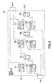
- the fast Hadamard transform device of the invention includes shift register units 20 1 - 20 n , n in number, and butterfly computation units 21 1 - 21 n/2 , n/2 in number, to perform n-th order fast Hadamard transform of p of quantization bits.
- Each of shift register units 20 1 - 20 n includes two input terminals DIN and LIN, and two output terminals DOUT and LOUT. To the DIN, n elements of input data V 1 - V n are supplied, and from the DOUT, n elements of output data W 1 - W n are supplied. The input data V1 - Vn which are supplied to the DIN are then supplied to the butterfly computation unit as serial data bit by bit. The bit computed by the butterfly computation unit is supplied to the LIN.
- Each of the shift register units 20 1 - 20 n shares an input latch and an output latch by preparing a selector and inputs the input data V 1 - V n from DIN at a predetermined input timing.
- the input data are then transformed to serial data at the shift register unit and addition or subtraction is performed on the serial data by the butterfly computation unit bit by bit. Consequently, the result from the operation is supplied from the DOUT at predetermined output timing as output data W 1 - W n .
- the butterfly computation unit includes two input terminals ADDIN and SUBIN, and two output terminals ADDOUT and SUBOUT.
- the unit performs butterfly computation on the input data from the LOUT of the shift register unit and supplies the result to the LIN of the shift register unit.
- the illustrated fast Hadamard transform device includes shift register units 20 1 - 20 8 and butterfly computation units 21 1 - 21 4 .
- each of Input signals V 1 - V 8 is supplied to the corresponding DIN of the shift register units 20 1 - 20 8 and each of output signals W 1 - W 8 is supplied from the corresponding DOUT of the shift register units 20 1 - 20 8 .
- the LOUT of the shift register unit 20 2q-1 (1 ⁇ q ⁇ 4, q is a natural number) is connected to the ADDIN of the butterfly computation unit 21 q . Also, the LOUT of the shift register unit 20 2q is connected to the SUBIN of the butterfly computation unit 21 q .
- the ADDOUT of the butterfly computation unit 21 r (1 ⁇ r ⁇ 4, r is a natural number) is connected to the LIN of the shift register unit 20 r .
- SUBOUT of the butterfly computation unit 21 r is connected to the LIN of the shift register unit 20 r+4 .
- the shift register unit 20 shown in Fig. 4 includes m of 1 bit flip flop circuits 30 1 - 30 m , m of input switches 31 1 - 31 m , and m of output switches 32 1 - 32 m .
- m is "p + log 2 n".
- Each of the flip flop circuits 301 - 30m latches an input signal of a D terminal at a predetermined latch clock and outputs the signal from a Q terminal.
- Each of the input switches 31 1 - 31 m outputs an input signal entered from an IN terminal to an O 1 terminal or an O 2 terminal in according to a predetermined input switch signal.
- Each of the output switches 32 1 - 32 m inputs an input signal from an l 1 terminal or an l 2 terminal in according to a predetermined output switch signal and outputs the signal from an OUT terminal.
- a signal from LIN is supplied to an IN terminal of the input switch 31 1 .
- a bit of DOUT is supplied from an O 1 terminal of the input switch 31 1 .
- An O 2 terminal of the input switch 31 1 is connected to an I 2 terminal of the output switch 32 1 .
- a most significant bit (MSB) of DIN is supplied to an I 1 terminal of the output switch 32 1 .
- An OUT terminal of the output switch 32 1 is connected to a D terminal of the flip flop circuit 30 1 .
- each of IN terminals of the input switches 31 2 - 31 7 the corresponding Q terminal of the flip flop circuits 30 1 - 30 6 , which reside the former step of the input switches, is connected.
- Signal from each of O 1 terminals of the input switches 31 2 - 31 7 are supplied as a bit of the DOUT.
- Each of O 2 terminals of the input switches 31 2 - 31 7 is connected to the corresponding I 2 terminal of the output switches 32 2 -32 7 .
- Each of bits from the next to the MSB to the least significant bit (LSB) of the DIN is entered to one of I 1 , terminals of the output switches 32 2 - 32 7 in order.
- OUT terminals of the output switches 32 2 - 32 7 are connected to the corresponding D terminal of the flip flop circuits 30 2 -30 7 .
- a Q terminal of the flip flop circuit 30 7 is supplied as LOUT.
- Such configuration of flip flop circuit keeps transform result bit by bit at each step of n-th order fast Hadamard transform.
- the input switch and the output switch controls flow of signals when the signals are supplied to the fast Hadamard transform device of the embodiment or when the signals are supplied as operation results. That is, each of the output switches 32 1 - 32 7 connects the I 1 terminal to the OUT terminal by the input switch signal at the predetermined signal input timing, and supplies an input signal from the DIN to one of the flip flop circuits 30 1 - 30 7 . Also, each of the input switches 31 1 - 31 7 connects the IN terminal to the O 1 terminal by the output switch signal at the predetermined signal output timing, and supplies a result from the butterfly computation entered from the LIN as DOUT.
- each of the input switches 311 - 317 connects the IN terminal to the 02 terminal
- each of the output switches 321 - 327 connects the 12 terminal to the OUT terminal
- signals are shifted at the flip flop circuits 301 - 307 by a bit for each predetermined latch clock and consecutively supplied to the butterfly computation unit as LOUT.
- the butterfly computation unit 21 shown in Fig. 5 includes an adder 40 having a bit of carry input/output, a subtractor 41 having a bit of borrow input/output, a flip flop circuit 42 having a bit of reset, and a flip flop circuit 43 having a bit of set.
- a signal which is supplied from the shift register unit to an ADDIN is supplied to an ADD 0 terminal of the adder 40 and to an ADD 0 terminal of the subtractor 41. Also, a signal which is supplied from the shift register unit to a SUBIN is supplied to an ADD 1 terminal of the adder 40 and to an SUB 0 terminal of the subtractor 41.
- the adder 40 outputs to the OUT terminal a result from adding of a bit from the ADDO terminal, a bit from the ADD1 terminal, and a carry bit from the CIN terminal, and outputs an output carry bit to the COUT terminal.
- the result of adding from the OUT terminal is supplied to the shift register unit as ADDOUT.
- the COUT terminal is connected to a D terminal of the flip flop circuit 42, and a Q terminal of the circuit 42 is connected to the CIN terminal of the adder 40.
- the subtractor 41 subtracts using a bit from the ADD0 terminal, a bit from the SUBO terminal, and a borrow bit from the BIN terminal and outputs the subtracting result to the OUT terminal. Further, the subtractor 41 outputs a borrow bit to the BOUT terminal.
- the subtracting result from the OUT terminal is supplied to the shift register unit as SUBOUT.
- the BOUT terminal is connected to a D terminal of the flip flop circuit 43, and a Q terminal of the flip flop circuit 43 is connected to the BIN terminal of the subtractor 41.
- the flip flop circuit 42 outputs "0" in response to a reset signal entered into an R terminal at an initial status, and performs, at a normal status, carry computation of a bit by delaying a carry bit by a clock of a latch clock and supplying the carry bit to the adder 40.
- the flip flop circuit 43 outputs "1" in response to a set signal entered into an S terminal at an initial status, and performs, at a normal status, borrow computation of a bit by delaying a borrow bit by a clock of a latch clock and supplying the borrow bit to the subtractor 41.
- Fig. 8 five lines (a) to (e) are shown.
- the top line (a) shows a timing of latch clock and the second line (b) shows an input timing of an input vector.
- the third line (c) shows an output timing of signals from the fast Hadamard transform device, and the forth line (d) shows a switching timing between an input switch and an output switch.
- the last line (e) shows a reset timing of the adder of the butterfly computation unit and a set timing of the subtractor of the butterfly computation unit.
- Each of the input vectors V 0 - V 7 include bits b 3 , b 2 , b 1 , and b 0 from the MSB side.
- the input signals 50 are then entered from LOUT of the corresponding shift register unit to the corresponding butterfly computation unit from the LSB side.
- b 3 of the DIN is entered into an I 1 terminal of the input switch 32 4
- b 2 of the DIN is entered into an I 1 terminal of the input switch 32 5
- b 1 of the DIN is entered into an I, terminal of the input switch 32 6
- b 0 of the DIN is entered into an I 1 terminal of the input switch 32 7 .
- Seven input switches are prepared for seven bits, this is because that carry occurs by the butterfly computation unit, thus, when the signals are entered, zero is given to each high order three bits including MSB. Therefore, when the signals are entered, zero is set to the l 1 terminals of the input switches 32 1 - 32 3 .
- the input switch signal 51 is entered into the input switches 32 1 - 32 7 .
- the input switch signal 51 is low level "L”
- the l 1 terminal and the OUT terminal are connected, and an input signal supplied to the l 1 terminal is entered to the D terminal of the corresponding one of the flip flop circuits 30 1 - 30 7 .
- the output switch signal is supposed to be entered to the output switches 31 1 - 31 7 at the same timing as the input switch signal 51, when the output signal is low level "L", in each of the output switches 31 1 - 31 7 , the IN terminal and the O 1 terminal are connected, and an input signal supplied to the IN terminal is entered to the DOUT terminal.
- the signals of the DOUT terminal are supplied as output signals 52 of results from the fast Hadamard transform of the last cycle. Also, as shown in Fig. 8, line (e), the flip flop circuits 42 and 43 of the butterfly computation unit are initialized since the reset signal and the set signal are entered into the butterfly computation unit (clear 53).
- V 1 + V 2 supplied from the ADDOUT is shown as follows.
- parallel-serial transform is performed by the flip flop of the shift register, and addition/subtraction is performed in "log 2 n * (p + log 2 n))" clocks.
- eighth order Hadamard transform of the input vector can be completed in twenty one clocks.
- line (d) for each twenty one clocks, switching between the input switches and the output switches is performed in response to the switch signal, quantized data stored in the flip flop circuit of the shift register are supplied as DOUT and next input vector is entered.
- the fast Hadamard transform device of the invention includes n of shift register units each of which is the same configuration for each n elements of input data having quantized bit number p, and is composed of "p + log 2 n" steps of one bit shift registers with switches capable of sharing the input latches and the output latches, and n/2 butterfly computation units each of which performs addition/subtraction bit by bit.
- the number of latches is reduced to 1/3, scale of circuits can be reduced to 1/"3 * the number of quantized bits", although the conventional device requires a plurality of sets each of which includes a plurality of adders and subtractors, and a plurality of bits of latch register.
- the fast Hadamard transform device of the invention higher speed operation can be performed since a circuit configuration of the device is sophisticatedly simplified and operation can be performed bit by bit. Thereby, the device can be operated at higher latch clock.
Landscapes
- Engineering & Computer Science (AREA)
- Computer Networks & Wireless Communication (AREA)
- Signal Processing (AREA)
- Theoretical Computer Science (AREA)
- Complex Calculations (AREA)
- Compression, Expansion, Code Conversion, And Decoders (AREA)
- Synchronisation In Digital Transmission Systems (AREA)
Applications Claiming Priority (2)
| Application Number | Priority Date | Filing Date | Title |
|---|---|---|---|
| JP36585799 | 1999-12-24 | ||
| JP36585799A JP3716695B2 (ja) | 1999-12-24 | 1999-12-24 | 高速アダマール変換器 |
Publications (2)
| Publication Number | Publication Date |
|---|---|
| EP1111804A2 true EP1111804A2 (de) | 2001-06-27 |
| EP1111804A3 EP1111804A3 (de) | 2003-09-24 |
Family
ID=18485298
Family Applications (1)
| Application Number | Title | Priority Date | Filing Date |
|---|---|---|---|
| EP20000128244 Withdrawn EP1111804A3 (de) | 1999-12-24 | 2000-12-21 | Schnelle Hadamard-Transformationsvorrichtung für CDMA-Übertragungssysteme |
Country Status (6)
| Country | Link |
|---|---|
| US (1) | US6732130B2 (de) |
| EP (1) | EP1111804A3 (de) |
| JP (1) | JP3716695B2 (de) |
| KR (1) | KR100354285B1 (de) |
| CN (1) | CN1302126A (de) |
| BR (1) | BR0006539A (de) |
Families Citing this family (17)
| Publication number | Priority date | Publication date | Assignee | Title |
|---|---|---|---|---|
| US20030050944A1 (en) * | 2001-08-21 | 2003-03-13 | Olivier Gay-Bellile | Device for computing discrete transforms |
| KR100800897B1 (ko) * | 2001-10-27 | 2008-02-04 | 삼성전자주식회사 | 고속 하다마드 변환 장치 및 방법 |
| US7188132B2 (en) * | 2001-12-25 | 2007-03-06 | Canon Kabushiki Kaisha | Hadamard transformation method and apparatus |
| KR100846485B1 (ko) * | 2002-04-09 | 2008-07-17 | 삼성전자주식회사 | 하다마드 트랜스폼 방법 및 장치 |
| WO2004002037A1 (fr) * | 2002-06-21 | 2003-12-31 | Linkair Communications,Inc. | Procede pour etaler le spectre de canaux multicodes pour des codes ls |
| JP3902990B2 (ja) * | 2002-07-02 | 2007-04-11 | キヤノン株式会社 | アダマール変換処理方法及びその装置 |
| US7003536B2 (en) * | 2002-08-15 | 2006-02-21 | Comsys Communications & Signal Processing Ltd. | Reduced complexity fast hadamard transform |
| US6996163B2 (en) * | 2003-03-27 | 2006-02-07 | Arraycomm, Inc. | Walsh-Hadamard decoder |
| CN1937451B (zh) * | 2005-09-19 | 2010-05-12 | 中兴通讯股份有限公司 | 一种快速哈达玛变换装置 |
| US7555514B2 (en) * | 2006-02-13 | 2009-06-30 | Atmel Corportation | Packed add-subtract operation in a microprocessor |
| US20080288568A1 (en) * | 2007-05-14 | 2008-11-20 | Hou Hsieh S | Low power Fast Hadamard transform |
| JP4933405B2 (ja) * | 2007-11-13 | 2012-05-16 | キヤノン株式会社 | データ変換装置及びその制御方法 |
| US8228971B2 (en) * | 2008-07-29 | 2012-07-24 | Agere Systems Inc. | Technique for searching for a preamble signal in a spread spectrum signal using a fast Hadamard transform |
| CN101894095B (zh) * | 2010-02-08 | 2015-08-12 | 北京韦加航通科技有限责任公司 | 快速哈达玛变换装置及方法 |
| CN101841711B (zh) * | 2010-04-17 | 2012-01-04 | 上海交通大学 | 用于视频解码的反量化装置及其实现方法 |
| CN102709826B (zh) * | 2012-06-25 | 2016-01-20 | 河南省电力公司南阳供电公司 | 变压器散热管蝶形阀维修装置及维修方法 |
| US8842665B2 (en) | 2012-08-17 | 2014-09-23 | Lsi Corporation | Mixed radix fast hadamard transform for communication systems |
Family Cites Families (7)
| Publication number | Priority date | Publication date | Assignee | Title |
|---|---|---|---|---|
| JPS5737925A (en) | 1980-08-14 | 1982-03-02 | Matsushita Electric Ind Co Ltd | High-speed hadamard converter |
| JPH05233681A (ja) | 1992-02-21 | 1993-09-10 | Sony Corp | アダマール変換回路 |
| JPH06301711A (ja) | 1993-04-14 | 1994-10-28 | Mitsubishi Electric Corp | 高速アダマール変換器 |
| US5561618A (en) * | 1993-12-22 | 1996-10-01 | Qualcomm Incorporated | Method and apparatus for performing a fast Hadamard transform |
| US5784293A (en) * | 1994-11-03 | 1998-07-21 | Motorola, Inc. | Apparatus and method for determining transmitted modulation symbols |
| KR970011794B1 (ko) * | 1994-11-23 | 1997-07-16 | 한국전자통신연구원 | 메모리 소자를 이용한 하다마드 변환기 |
| US6311202B1 (en) * | 1999-03-12 | 2001-10-30 | Lucent Technologies Inc. | Hardware efficient fast hadamard transform engine |
-
1999
- 1999-12-24 JP JP36585799A patent/JP3716695B2/ja not_active Expired - Fee Related
-
2000
- 2000-12-21 BR BR0006539A patent/BR0006539A/pt not_active IP Right Cessation
- 2000-12-21 EP EP20000128244 patent/EP1111804A3/de not_active Withdrawn
- 2000-12-22 US US09/745,649 patent/US6732130B2/en not_active Expired - Fee Related
- 2000-12-23 KR KR1020000081107A patent/KR100354285B1/ko not_active IP Right Cessation
- 2000-12-25 CN CN00136131A patent/CN1302126A/zh active Pending
Non-Patent Citations (1)
| Title |
|---|
| BI GUOAN ET AL: "Hardware structure for Walsh-Hadamard transforms" ELECTRONICS LETTERS, IEE STEVENAGE, GB, vol. 34, no. 21, 15 October 1998 (1998-10-15), pages 2005-2006, XP006010460 ISSN: 0013-5194 * |
Also Published As
| Publication number | Publication date |
|---|---|
| US20010007110A1 (en) | 2001-07-05 |
| BR0006539A (pt) | 2001-07-24 |
| US6732130B2 (en) | 2004-05-04 |
| CN1302126A (zh) | 2001-07-04 |
| JP2001184337A (ja) | 2001-07-06 |
| JP3716695B2 (ja) | 2005-11-16 |
| KR100354285B1 (ko) | 2002-09-28 |
| KR20010062661A (ko) | 2001-07-07 |
| EP1111804A3 (de) | 2003-09-24 |
Similar Documents
| Publication | Publication Date | Title |
|---|---|---|
| EP1111804A2 (de) | Schnelle Hadamard-Transformationsvorrichtung für CDMA-Übertragungssysteme | |
| Peled et al. | A new hardware realization of digital filters | |
| US6618698B1 (en) | Clustered processors in an emulation engine | |
| EP1078457B1 (de) | Sequenz-generator | |
| US6009259A (en) | Emulation System | |
| US5761265A (en) | Parallel architecture for generating pseudo-random sequences | |
| US5506796A (en) | Digital signal processing circuit selectively operable in either a normal or a pseudorandom noise generative mode | |
| US4325129A (en) | Non-linear logic module for increasing complexity of bit sequences | |
| US6959407B2 (en) | Context save and restore using test scan chains | |
| US7028062B2 (en) | FIR filter, method of operating the same, semiconductor integrated circuit including FIR filter, and communication system for transmitting data filtered by FIR filter | |
| US6240062B1 (en) | Fast fourier transform calculating apparatus and fast fourier transform calculating method | |
| US7039091B1 (en) | Method and apparatus for implementing a two dimensional correlator | |
| JP2917962B2 (ja) | M系列を任意にシフトする回路 | |
| KR100913467B1 (ko) | 병렬 순환 중복 검사 코드 발생 시스템 및 방법 | |
| US20030169939A1 (en) | Apparatus and method for Fast Hadamard Transforms | |
| US7024606B2 (en) | Method of generating test pattern for integrated circuit | |
| US6735189B1 (en) | Flexible CDMA combiner | |
| Myers et al. | HANNIBAL: A VLSI building block for neural networks with on-chip backpropagation learning | |
| KR20000028978A (ko) | 레이크 수신기용 횡 상관기 구조 | |
| US7366747B2 (en) | Digital filter circuit and data processing method | |
| US6470369B1 (en) | Euclid mutual division arithmetic circuit and processing circuit | |
| SU1520511A1 (ru) | Вычислительное устройство дл поворота вектора | |
| US6661256B2 (en) | Race logic circuit | |
| US8832172B1 (en) | Optimal FPGA based hadamard detection | |
| RU2051407C1 (ru) | Способ суммирования цифровых сигналов |
Legal Events
| Date | Code | Title | Description |
|---|---|---|---|
| PUAI | Public reference made under article 153(3) epc to a published international application that has entered the european phase |
Free format text: ORIGINAL CODE: 0009012 |
|
| AK | Designated contracting states |
Kind code of ref document: A2 Designated state(s): AT BE CH CY DE DK ES FI FR GB GR IE IT LI LU MC NL PT SE TR |
|
| AX | Request for extension of the european patent |
Free format text: AL;LT;LV;MK;RO;SI |
|
| PUAL | Search report despatched |
Free format text: ORIGINAL CODE: 0009013 |
|
| AK | Designated contracting states |
Kind code of ref document: A3 Designated state(s): AT BE CH CY DE DK ES FI FR GB GR IE IT LI LU MC NL PT SE TR |
|
| AX | Request for extension of the european patent |
Extension state: AL LT LV MK RO SI |
|
| 17P | Request for examination filed |
Effective date: 20030904 |
|
| 17Q | First examination report despatched |
Effective date: 20031128 |
|
| STAA | Information on the status of an ep patent application or granted ep patent |
Free format text: STATUS: THE APPLICATION HAS BEEN WITHDRAWN |
|
| 18W | Application withdrawn |
Effective date: 20040114 |