EP1111661A2 - Hochtemperatur elektrostatischer Halter - Google Patents
Hochtemperatur elektrostatischer Halter Download PDFInfo
- Publication number
- EP1111661A2 EP1111661A2 EP00311471A EP00311471A EP1111661A2 EP 1111661 A2 EP1111661 A2 EP 1111661A2 EP 00311471 A EP00311471 A EP 00311471A EP 00311471 A EP00311471 A EP 00311471A EP 1111661 A2 EP1111661 A2 EP 1111661A2
- Authority
- EP
- European Patent Office
- Prior art keywords
- chuck body
- chuck
- heat transfer
- substrate
- plenum
- Prior art date
- Legal status (The legal status is an assumption and is not a legal conclusion. Google has not performed a legal analysis and makes no representation as to the accuracy of the status listed.)
- Granted
Links
Images


Classifications
-
- H—ELECTRICITY
- H01—ELECTRIC ELEMENTS
- H01L—SEMICONDUCTOR DEVICES NOT COVERED BY CLASS H10
- H01L21/00—Processes or apparatus adapted for the manufacture or treatment of semiconductor or solid state devices or of parts thereof
- H01L21/67—Apparatus specially adapted for handling semiconductor or electric solid state devices during manufacture or treatment thereof; Apparatus specially adapted for handling wafers during manufacture or treatment of semiconductor or electric solid state devices or components ; Apparatus not specifically provided for elsewhere
- H01L21/683—Apparatus specially adapted for handling semiconductor or electric solid state devices during manufacture or treatment thereof; Apparatus specially adapted for handling wafers during manufacture or treatment of semiconductor or electric solid state devices or components ; Apparatus not specifically provided for elsewhere for supporting or gripping
- H01L21/6831—Apparatus specially adapted for handling semiconductor or electric solid state devices during manufacture or treatment thereof; Apparatus specially adapted for handling wafers during manufacture or treatment of semiconductor or electric solid state devices or components ; Apparatus not specifically provided for elsewhere for supporting or gripping using electrostatic chucks
-
- Y—GENERAL TAGGING OF NEW TECHNOLOGICAL DEVELOPMENTS; GENERAL TAGGING OF CROSS-SECTIONAL TECHNOLOGIES SPANNING OVER SEVERAL SECTIONS OF THE IPC; TECHNICAL SUBJECTS COVERED BY FORMER USPC CROSS-REFERENCE ART COLLECTIONS [XRACs] AND DIGESTS
- Y10—TECHNICAL SUBJECTS COVERED BY FORMER USPC
- Y10T—TECHNICAL SUBJECTS COVERED BY FORMER US CLASSIFICATION
- Y10T279/00—Chucks or sockets
- Y10T279/23—Chucks or sockets with magnetic or electrostatic means
Definitions
- the invention relates to an electrostatic chuck (ESC) useful for processing substrates such as semiconductor wafers.
- the ESC can be used to support a semiconductor substrate in a plasma reaction chamber wherein etching or deposition processes are carried out.
- the ESC is especially useful for high temperature plasma etching of materials such as platinum which are not volatile at low temperatures.
- Vacuum processing chambers are generally used for etching and chemical vapor depositing (CVD) of materials on substrates by supplying an etching or deposition gas to the vacuum chamber and application of an RF field to the gas to energize the gas into a plasma state.
- Examples of parallel plate, transformer coupled plasma (TCP) which is also called inductively coupled plasma (ICP), and electron-cyclotron resonance (ECR) reactors are disclosed in commonly owned U.S. Patent Nos. 4,340,462; 4,948,458; and 5,200,232.
- Vacuum processing chambers are typically designed to meet performance specifications which depend on the process to be carried out therein. Thus, the particular plasma generating source, vacuum pumping arrangement and substrate support associated with the particular processing chamber must be customized or specially designed to meet the performance specifications.
- Substrates are typically held in place within the vacuum chamber during processing by substrate holders.
- Conventional substrate holders include mechanical clamps and electrostatic clamps (ESC). Examples of mechanical clamps and ESC substrate holders are provided in commonly owned U.S. Patent No. 5,262,029 and commonly owned U.S. Application Serial No. 08/401,524 filed on March 10, 1995.
- Substrate holders in the form of an electrode can supply radiofrequency (RF) power into the chamber, as disclosed in U.S. Patent No. 4,579,618.
- RF radiofrequency
- Substrates including flat panel displays and smaller substrates can be cooled by the substrate holder during certain processing steps. Such cooling is performed by the application of an inert gas, such as helium, between the substrate holder and the opposed surface of the substrate.
- an inert gas such as helium
- the cooling gas is typically supplied to channels or a pattern of grooves in the substrate holder and applies a back pressure to the substrate.
- Electrostatic chucks of the monopolar type utilize a single electrode. For instance, see U.S. Patent No. 4,665,463.
- Electrostatic chucks of the bipolar type utilize mutual attraction between two electrically charged capacitor plates which are separated by a dielectric layer. For instance, see U.S. Patent Nos. 4,692,836 and 5,055,964.
- Substrate supports for vacuum processing chambers are typically mounted on a bottom wall of the chamber making servicing and replacement of the substrate support difficult and time consuming. Examples of such bottom mounted substrate supports can be found in U.S. Patent Nos. 4,340,462; 4,534,816; 4,579,618; 4,615,755; 4,948,458; 5,200,232; and 5,262,029.
- a cantilevered support arrangement is described in commonly owned U.S. Patent Nos.5,820,723 and 5,948,704.
- EP'644 discloses an aluminum nitride chuck body having an RF metallic electrode plate which is perforated with holes to form a mesh and a heater embedded therein, the chuck body being supported on an alumina cylinder such that the outer periphery of the chuck body extends beyond the cylinder.
- the '803 patent discloses a chuck body of silicon nitride or alumina having an electrical grid of Mo, W, W-Mo and a Mo heater coil wire embedded therein, the chuck body being supported by a Mo heat choke cylinder which surrounds a Cu or Al water cooled cooling plate in thermal contact with the chuck body by a thermal grease which allows differential expansion between the chuck body and the cooling plate.
- the '359 patent describes a chuck operational at temperatures on the order of 500°C, the chuck including sapphire (single crystal Al 2 O 3 ) layers brazed to opposite sides of a niobium electrode and that assembly brazed to a metal base plate.
- the '334 patent describes a chuck for use at temperatures in excess of 175°C, the chuck including polyimide films on either side of a monopolar or bipolar electrode with the lower polyimide film self adhered to a stainless steel platen.
- the '273 patent discloses a layered chuck body including an aluminum nitride top layer, an electrode, an aluminum nitride layer, a metal plate, a heater, a metal plate and an aluminum composite, the chuck body being supported by a cylinder such that the outer periphery of the chuck body extends beyond the cylinder.
- ESC designs use a heat conduction gas such as helium to enhance conduction of heat between adjacent surfaces of the wafer support.
- a heat conduction gas such as helium to enhance conduction of heat between adjacent surfaces of the wafer support.
- U.S. Patent No. 5,155,652 describes an ESC having layers including an upper pyrolytic boron nitride layer or optionally polyimide, alumina, quartz, or diamond, an electrostatic pattern layer comprised of a boron nitride substrate and a conductive pattern of pyrolytic graphite thereon, a heater layer comprised of a boron nitride substrate and a conductive pattern of pyrolytic graphite thereon, and a heat sink base of KOVAR (NiCoFe alloy with 29%Ni, 17%Co and 55%Fe).
- KOVAR NiCoFe alloy with 29%Ni, 17%Co and 55%Fe
- the heat sink base includes water cooling channels in a lower portion thereof and chambers in an upper surface thereof which can be maintained under vacuum during heatup of the chuck or filled with helium to aid in cooling of a wafer supported by the chuck.
- U.S. Patent No. 5,221,404 describes a support table comprised of an upper member which supports a wafer and a lower member which includes a liquid passage for temperature control of the wafer, the upper member including an ESC constituted by a copper electrode between polyimide sheets and a gap between contacting surfaces of the upper and lower members being supplied a heat conduction gas.
- 5,835,334 describes a high temperature chuck wherein helium is introduced between contacting surfaces of a lower aluminum electrode and an electrode cap which is bolted to the lower electrode, the electrode cap comprising anodized aluminum or diamond coated molybdenum.
- a protective alumina ring and O-ring seals minimize leakage of the coolant gas between the electrode cap and the lower electrode.
- the electrode cap includes liquid coolant channels for circulating a coolant such as ethylene glycol, silicon oil, fluorinert or a water/glycol mixture and the lower electrode includes a heater for heating the chuck to temperatures of about 100 - 350°C. To prevent cracking of the anodization due to differential thermal expansion, the electrode cap is maintained at temperatures no greater than 200°C. In the case of the diamond coated molydenum electrode cap, the chuck can be used at higher temperatures.
- the invention provides an electrostatic chuck useful in a high temperature vacuum processing chamber comprising a chuck body, a heat transfer body and an expansion joint therebetween.
- the chuck body comprises an electrostatic clamping electrode and optional heater element, the electrode being adapted to electrostatically clamp a substrate such as a semiconductor wafer on an outer surface of the chuck body.
- the heat transfer body is separated from the chuck body by a plenum located between spaced apart surfaces of the chuck body and the heat transfer body, the heat transfer body being adapted to remove heat from the chuck body by heat conductance through a heat transfer gas in the plenum.
- the expansion joint attaches an outer periphery of the chuck body to the heat transfer body, the expansion joint accommodating differential thermal expansion of the chuck body and the heat transfer body while maintaining a hermetic seal during thermal cycling of the chuck body.
- the heat transfer body comprises a cooling plate having at least one coolant passage therein in which coolant can be circulated to maintain the chuck body at a desired temperature and the plenum is an annular space extending over at least 50% of the underside of the chuck body.
- the heat transfer body includes a gas supply passage through which heat transfer gas flows into the annular space.
- the chuck body includes gas passages extending between the plenum and the outer surface of the chuck body. The gas passages can be provided in any suitable arrangement.
- the gas passages can be located adjacent to the expansion joint so that the heat transfer gas flows from the plenum to the underside of an outer periphery of the substrate during processing thereof.
- the chuck body comprises a metallic material such as aluminum or alloy thereof or a ceramic material such as aluminum nitride.
- the expansion joint can comprise a thin metal section brazed to the ceramic chuck body.
- Lift pins can be used to raise and lower a substrate.
- the heat transfer body can include lift pins such as cable actuated lift pins mounted thereon, the lift pins being movable towards and away from the chuck body such that the lift pins travel through holes in the chuck body to raise and lower a substrate onto and off of the chuck body.
- the expansion joint can include a mounting flange adapted to attach to the heat transfer body and a heat choke such as a single or multi-piece flexible metal part.
- the heat choke can include inner and outer annular sections interconnected by a curved section, the inner annular section being attached to the chuck body and the outer annular section being attached to the mounting flange.
- the expansion joint can also include a connecting member such as a thin ring attached at one end to an outer periphery of the chuck body by a joint such as a mechanical joint or metallurgical joint such as a brazed joint, the connecting member being of a metal having a coefficient of thermal expansion close enough to that of the chuck body to prevent failure of the joint during thermal cycling of the chuck body.
- the expansion joint can include a thermal expansion section which abuts an outer edge of the chuck body, the thermal expansion section being thermally expandable and contractible to accommodate changes in dimensions of the chuck body.
- the chuck body can include a ceramic or metallic tubular section extending from a central portion of the underside of the chuck body such that an outer surface of the tubular section defines a wall of the plenum, the tubular section being supported in floating contact with the heat transfer body with a hermetic seal therebetween.
- the interior of the tubular section can include power supplies supplying RF and DC power to the clamping electrode and AC power to the heater element, and/or a temperature measuring arrangement for monitoring temperature of the chuck body.
- the chuck is a replaceable electrostatic chuck for a vacuum processing chamber wherein the chuck includes a chuck body and an expansion joint.
- the chuck comprises an electrode having an electrical contact attachable to an electrical power supply which energizes the electrode sufficiently to electrostatically clamp a substrate on an outer surface of the chuck body.
- the expansion joint includes a first portion attached to an outer periphery of the chuck body and a second portion removably attachable to a heat transfer body such that a plenum is formed between spaced apart surfaces of the chuck body and the heat transfer body.
- the invention also provides a method of processing a substrate in a vacuum process chamber wherein the substrate is electrostatically clamped on a chuck body comprising a clamping electrode and an expansion joint attaching an outer periphery of the chuck body to a heat transfer body such that a plenum is formed between spaced apart surfaces of the chuck body and the heat transfer body, the method comprising clamping a substrate on an outer surface of the chuck body by energizing the electrode, supplying a heat transfer gas to the plenum, the heat transfer gas in the plenum passing through gas passages in the chuck body to a gap between an underside of the substrate and the outer surface of the chuck body, removing heat from the chuck body by heat conductance through the heat transfer gas supplied to the plenum, and processing the substrate.
- the method further comprises supplying process gas to the chamber and energizing the process gas into a plasma and etching an exposed surface of the substrate with the plasma during the processing step.
- an exposed surface of the substrate can be coated during the processing step.
- the process gas can be energized into the plasma by any suitable technique such as supplying radiofrequency energy to an antenna which inductively couples the radiofrequency energy into the chamber.
- the substrate can be heated by supplying power to a heater element embedded in the chuck body. Prior to clamping the substrate, the substrate can be lowered onto the outer surface of the chuck body with lift pins mounted on the heat transfer body, the lift pins passing through openings in an outer portion of the chuck body.
- the method can include circulating a liquid coolant in the heat transfer body. Temperature changes in the substrate can be monitored with a temperature sensor supported by the heat transfer body and extending through a hole in the chuck body. In the case of plasma etching a layer of platinum during the processing step, the substrate can be heated to a temperature of over 200°C.
- the method it is possible to achieve a desired heat distribution across the chuck body by removing heat from the chuck body through multiple heat paths. Further, it is possible to adjust the amount of heat removed through these heat paths by changing the pressure of the heat transfer gas in the plenum. For instance, since the ceramic or metallic tubular extension at a central portion of the underside of the chuck body conducts heat from the chuck body to the heat transfer body, the method can include adjusting pressure of the heat transfer gas in the plenum so that heat removed through a first heat path provided by the heat transfer gas in the plenum balances heat removed through a second heat path provided by the expansion joint and heat removed through a third heat path provided by the tubular extension.
- the invention provides an electrostatic chuck useful for clamping substrates such as semiconductor wafers during processing thereof in a vacuum processing chamber such as a plasma etch reactor.
- the electrostatic chuck can be used for other purposes such as clamping substrates during chemical vapor deposition, sputtering, ion implantation, resist stripping, etc.
- the chuck includes a clamping electrode and an optional heating element which can be used to maintain the substrate supported on the chuck at elevated temperatures above 80°C (the upper limit of certain conventional chucks is 60°C), preferably over 200°C, for example 250 to 500°C.
- the chuck can be used to support a wafer during chemical vapor deposition or plasma etching of materials wherein it is necessary to heat the substrate to temperatures on the order of about 150°C and above.
- the chuck includes an expansion joint design which provides the chuck with high temperature functionality in a small package.
- the expansion joint creates a plenum between spaced apart surfaces of an actively heated portion of the chuck and an actively cooled portion of the chuck.
- the plenum is filled with a heat transfer gas to conduct heat from the heated portion to the cooled portion of the chuck.
- the expansion joint design provides a small overall height of the chuck which makes the chuck compatible with tight system packaging requirements (footprint).
- a further advantage of the expansion joint is that thermal stresses can be accommodated between the heated and cooled portions of the chuck.
- a heat transfer gas such as helium can be supplied to targeted locations on the underside of the substrate without the need for a complicated arrangement of gas passages inside the chuck.
- a low volatility etch product can be removed from a substrate by a plasma etch process wherein the substrate is heated by the chuck.
- Such low volatility etch products can be formed during plasma etching of noble metals such as Pt, Pd, Ru and Ir, materials under consideration for the electrodes of capacitors using high-k dielectric materials.
- Such low volatility etch products remain on the substrate surface unless the substrate is heated sufficiently.
- platinum chloride formed during etching of platinum can be volatilized by heating the substrate to around 300°C.
- Conventional chucks used in low temperature etch processes are unsuited for such high temperature environments since they can undergo damaging thermal cycling which ruptures hermetic seals and/or causes failure of chuck materials.
- the chuck according to the invention solves these problems through use of the expansion joint design.
- the chuck body is made from a metallic or ceramic material having desired electrical and/or thermal properties.
- the chuck body can be made of aluminum or an aluminum alloy
- the chuck body can be made from one or more ceramic materials including nitrides such as aluminum nitride, boron nitride and silicon nitride, carbides such as silicon carbide and boron carbide, oxides such as alumina, etc. with or without fillers such as particles in the form of whiskers, fibers or the like or infiltrated metals such as silicon.
- a ceramic chuck body can be formed by various techniques.
- the ceramic material can be formed into a monolithic body by a powder metallurgical technique wherein ceramic power is formed into a chuck body shape such as by compacting or slip casting the powder with the clamping electrode, heater and power supply connections embedded therein, the chuck body being densified by sintering the powder.
- the chuck body can be formed from sheets of ceramic material which are overlaid with electrically conductive patterns for the clamping electrode, the heater and power feedthroughs incorporated therein, the layers being cofired to form the final chuck body.
- HTESC high temperature electrostatic chuck
- the HTESC according to the invention can offer better high temperature functionality and relatively low power requirements compared to conventional chuck assemblies wherein a cooling plate is integrated as a one-piece electrostatic chuck.
- the maximum operational temperature is limited to approximately 60°C.
- the HTESC of the present invention has been designed as a two-piece assembly, including an ESC portion such as a ceramic chuck body having an electrostatic clamping electrode embedded therein and a heat transfer body such as a cooling plate.
- an expansion joint in the form of heat break tubulations have been integrated into the ESC portion for thermally isolating the ESC portion from the cooling plate.
- the heat break tubulations significantly reduce conduction of heat from a peripheral edge of the ESC portion to the cooling plate, thereby allowing the ESC portion to reach temperatures as high as approximately 500°C without requiring the supply of a relatively large amount of power to a heater element embedded in the chuck body.
- the expansion joint provides a long operational life of the HTESC.
- the ESC portion can undergo extensive thermal expansion without damaging other parts of the HTESC.
- the heat break tubulations can be designed as a one-piece metal part or a multi-piece welded or brazed assembly which includes one or more thin-walled sections which allow thermal expansion and contraction of the ESC portion while minimizing heat transfer from the ESC portion to the cooling plate.
- the heat break tubulations accommodate differential thermal expansion between the ESC portion and the cooling plate, thereby minimizing stresses within the HTESC assembly and thus reducing the chance of premature failure of the HTESC assembly.
- the heat break tubulations can be designed in a manner which reduces stress at brazed joints within the HTESC assembly.
- the HTESC according to the present invention includes a simple arrangement which can selectively target portions of the substrate where more cooling is desired.
- the HTESC assembly includes a plenum between the ESC portion and the cooling plate and the plenum can serve the dual function of (1) withdrawing heat from the ESC portion by supplying a heat transfer gas to the plenum and (2) distributing heat transfer gas to select portions of the substrate through gas passages extending from the plenum to the outer surface of the ESC portion.
- gas distribution holes can be provided near the outer periphery of the ESC portion to enhance the cooling of the outer portion of the substrate.
- a complicated gas distribution arrangement is not necessary since the gas distribution holes can be formed by holes at desired locations in the support surface of the ESC portion.
- the use of the expansion joint in the HTESC assembly of the present invention can reduce manufacturing costs and/or simplify manufacture of the HTESC.
- the heat break tubulations thermally isolate the hot ESC portion from the cooling piate.
- standard low cost elastomer seals can be used at locations in contact with the cooling plate.
- the HTESC according to the invention is designed to provide a small overall height so that it can be used in vacuum chambers wherein the chuck is supported on a cantilevered support arm.
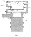
- Figures 1-3 illustrate examples of vacuum processing chambers 10, 24 into which the HTESC assembly of the present invention could be mounted. While the invention will be explained with reference to the chamber design shown in Figures 1-3, it will be appreciated by those skilled in the art that the HTESC assembly of the present invention can be used in any vacuum processing chamber wherein it is desired to electrostatically clamp a substrate.
- the HTESC assembly of the present invention could be used as part of a substrate support in processing chambers where various semiconductor plasma or non-plasma processing steps such as etching, deposition, resist stripping, etc. can be performed.
- the vacuum chamber 10 includes a cantilevered substrate support 12 extending inwardly from a sidewall of the chamber and a HTESC 14 is supported by the support.
- a service passage 18 containing service conduits opens into an interior of the support housing 16.
- the service conduits can be used to service the HTESC, e.g., supply DC power to a clamping electrode, supply RF power to the clamping electrode or a separate electrode which provides an RF bias to the substrate during processing thereof, supply AC power to a heater element, house cables for actuating lift pins, supply coolant for cooling the HTESC and/or the substrate, transmit electrical signals from sensors or monitoring equipment, etc.
- a mounting flange 20 and support arm 22 form an integral piece which can be removably mounted in an opening in the chamber, e.g., by mechanical fasteners with an O-ring and RF shielding interposed between opposed surfaces of the flange 20 and the chamber.
- gas within the chamber can be withdrawn through an opening 21 by a vacuum pump 23.
- Plasma can be generated in the chamber by a source of energy (not shown) mounted at the top of the chamber. That is, the top of the chamber is designed to support various types of plasma generating sources such as capacitive coupled, inductive coupled, microwave, magnetron, helicon, or other suitable plasma generating equipment.
- process gas can be supplied to the chamber by various types of gas supply arrangements such as a gas distribution plate (showerhead), one or more gas rings and/or gas injectors, or other suitable arrangement.
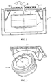
- FIG 2 illustrates a vacuum processing chamber 24 and a cantilevered substrate support 26 on which a chuck assembly 28 has been mounted.
- a substrate 30 is supported on a HTESC assembly 28 mounted on a substrate support 26.
- the substrate support 26 is at one end of a support arm 32 (shown in Figure 3) mounted in a cantilever fashion such that the entire substrate support/support arm assembly 26/32 can be removed from the chamber by passing the assembly through an opening (not shown) in the sidewall of the chamber 24.
- Process gas can he supplied to the chamber by any suitable arrangement such as a gas supply pipe 34 or a gas distribution plate 36 and the gas can be energized into a plasma state by an antenna 38 such as a planar coil which inductively couples Rf energy through a dielectric member 40.
- the antenna can be supplied RF energy by any suitable arrangement such as a conventional RF power generator 42 and a match network 44.
- a heat transfer gas such as helium can be supplied to the backside of the wafer through holes 46, as shown in Figure 3.
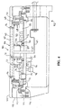
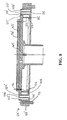
- FIG 4 shows a HTESC assembly 50 according to a first embodiment of the present invention wherein the HTESC assembly 50 is mounted on a cantilevered substrate support 52 in a vacuum processing chamber, as discussed above with reference to Figures 1-3.
- the HTESC assembly 50 is a two-piece design including a chuck body 56 and a heat transfer body 58.
- the chuck body 56 includes a clamping electrode 60, an optional heater element 62, an expansion joint 64, and a central tubular extension 66.
- the expansion joint 64 includes an annular mounting flange 68 which is removably attached to the heat transfer body 58 by bolts 70.
- the chuck body 56 is preferably made of a ceramic material exhibiting dielectric properties such as aluminum nitride.
- the expansion joint 64 and the heat transfer body 58 can be made of heat conducting metals such as aluminum, copper, titanium and alloys thereof, but a preferred material is a low heat conducting metal such as stainless steel, cobalt, nickel, molybdenum, zirconium or alloys thereof.
- the expansion joint 64 and the heat transfer body can be made of any materials compatible in a vacuum chamber in which semiconductor substrates are processed.
- the heat transfer body includes coolant passages and coolant such as water or other coolant can be supplied to the passages 72 by suitable conduits one of which is shown at 74.
- Electrical power can be supplied to the clamping electrode 60 and the heater element 62 by power supply lines in tubular extension 66.
- RF and DC power can be supplied to the clamping electrode by a rod 67, the bottom of which is connected to a strap 69.
- Temperature of the chuck body can be monitored with a temperature feedback assembly 71 in the tubular extension 66.
- a plenum 80 is provided between spaced apart surfaces 82 and 84 of the chuck body 56 and the heat transfer body 58.
- a heat transfer gas such as helium can be supplied to the plenum 80 by a gas conduit 76.
- the temperature of the substrate on the chuck body can be monitored with a fiberoptic element 77 supported in a fitting 78.
- any type of lift pin assembly can be used such as a pneumatically actuated lift pin assembly, according to a preferred embodiment a fitting mounted in a bore 79 can be used to support a cable actuated lift pin assembly.
- Elastomer seals 88 and 90 fitted in grooves in the heat transfer body 58 and an elastomer seal 89 fitted in a collar 91 surrounding tubular extension 66 provide vacuum seals between the expansion joint 64 and the heat transfer body 58 and between the tubular extension 66 and the heat transfer body 58.
- An elastomer seal 92 provides a vacuum seal between an underside of the heat transfer body 58 and a dielectric mounting plate 94 and an elastomer seal 96 provides a vacuum seal between an underside of the mounting plate 94 and the housing 54.
- a dielectric edge ring 98 (e.g., alumina, silicon nitride, quartz, etc.) overlies the mounting plate 94 and a dielectric focus ring 100 (e.g., alumina, silicon nitride, silicon carbide, etc.) overlies the edge ring 98 and surrounds the chuck body 56.
- a dielectric focus ring 100 e.g., alumina, silicon nitride, silicon carbide, etc.
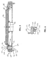
- Figure 5 shows details of the chuck body 56 with the expansion joint 64 attached thereto and Figure 6 is an enlarged view of a brazed joint (detail VI in Figure 5) between the chuck body 56 and the expansion joint 64.
- the expansion joint 64 includes the mounting flange 68, an outer annular section 102, and an inner annular section 104, the outer section 102 being connected to the flange 68 by a curved section 101 and the inner section 104 being connected to the outer section 102 by a curved section 106.
- the outer section 102 is separated from the flange 68 by an annular space 108 and the inner section 104 is separated from the outer section 102 by an annular space 110.
- the flange 68, the outer section 102 and the inner section 104 can be formed (e.g., machined, cast, forged, etc.) out of a single piece of metal such as stainless steel.
- the expansion joint can be made from a multi-piece welded or brazed assembly.
- the expansion joint can also include a thin metal ring 112 which is welded at its bottom to the bottom of the inner section 104 and brazed at its top to the underside of the chuck body 56.
- a small ceramic ring 114 can be brazed to adjoining surfaces of the chuck body and the ring 112.
- the ring 112 can be of a NiCoFe alloy such as KOVAR which has a similar coefficient of thermal expansion as aluminum nitride.
- a small gap 116 e.g., 0.002-0.004 inch
- the ceramic ring 114 is set back from the sidewall 122 such that a gap 118 is provided between the ring 112 and the inner section 104, the gap providing sufficient area to accommodate a brazed joint 124 between the ring 112 and the underside of the chuck body 56. If desired, the brazed joint can be replaced with a mechanical joint.
- the sidewall of the chuck body 56 presses against the inner section 104 and elastically deflects the inner and outer sections of the expansion joint.
- bending of the ring 112 and consequent stress on the brazed joint 124 can be minimized.
- less stress is placed on the welded joint between the ring 112 and the inner section 104.
- the curved sections 106 and 110 allow elastic deflection of the inner and outer sections of the expansion joint to accommodate thermal expansion and contraction of the chuck body 56.
- FIG 7 shows a HTESC assembly 50' according to a second embodiment of the present invention wherein the HTESC assembly 50' is mounted on a cantilevered substrate support 52 in a vacuum processing chamber, as discussed above with reference to Figures 1-3.
- the HTESC assembly 50' is a two-piece design including a chuck body 56' and a heat transfer body 58'.
- the chuck body 56' includes a clamping electrode 60', an optional heater element 62', an expansion joint 64', and a central tubular extension 66'.
- the expansion joint 64' includes an annular mounting flange 68' which is removably attached to the heat transfer body 58' by bolts 70.
- the chuck body 56' is preferably made of a ceramic material exhibiting dielectric properties such as aluminum nitride.
- the expansion joint 64' and the heat transfer body 58' can be made of heat conducting metals such as aluminum, copper, titanium and alloys thereof, but a preferred material is a low heat conducting metal such as stainless steel, cobalt, nickel, molybdenum, zirconium or alloys thereof.
- the chuck body 56', the expansion joint 64' and the heat transfer body can be made of any materials compatible in a vacuum chamber in which semiconductor substrates are processed.
- the heat transfer body 58' includes coolant passages 72 and coolant such as water or other coolant can be supplied to the passages 72 by conduits one of which is shown at 74.
- Electrical power can be supplied to the clamping electrode 60' and the heater element 62' by power supply lines in tubular extension 66'.
- RF and DC power can be supplied to the clamping electrode by a rod 67', the bottom of which is connected to a strap 69'.
- Temperature of the chuck body can be monitored with a temperature feedback assembly 71 in the tubular extension.
- a plenum 80 is provided between spaced apart surfaces 82 and 84 of the chuck body 56' and the heat transfer body 58'.
- a heat transfer gas such as helium can be supplied to the plenum 80 by a gas conduit 76.
- the temperature of the substrate on the chuck body can be monitored with a fiberoptic element 77 supported in a fitting 78.
- any type of lift pin assembly can be used such as a pneumatically actuated lift pin assembly, according to a preferred embodiment a fitting mounted in a bore 79 can be used to support a cable actuated lift pin.
- Elastomer seals 88, 89 and 90 fitted in grooves in the heat transfer body 58' and a casing 59 bolted to the heat transfer body 58' provide vacuum seals between the expansion joint 64' and the heat transfer body 58' and between the tubular extension 66' and the casing 59.
- An elastomer seal 92 provides a vacuum seal between an underside of the heat transfer body 58' and a dielectric mounting plate 94 and an elastomer seal 96 provides a vacuum seal between an underside of the mounting plate 94 and the housing 54.
- a dielectric edge ring 98 (e.g., alumina, silicon nitride, quartz, etc.) overlies the mounting plate 94 and a dielectric focus ring 100 (e.g., alumina, silicon nitride, silicon carbide, etc.) overlies the edge ring 98 and surrounds the chuck body 56'.
- a dielectric focus ring 100 e.g., alumina, silicon nitride, silicon carbide, etc.
- Figure 8 shows details of the chuck body 56' with the expansion joint 64' attached thereto.
- the expansion joint 64' includes the mounting flange 68', an outer annular section 102', and an inner annular section 104', the outer section 102' being connected to the flange 68' by a curved section 101' and the inner section 104' being connected to the outer section 102' by a curved section 106'.
- the outer section 102' is separated from the flange 68' by an annular space 108' and the inner section 104' is separated from the outer section 102' by an annular space 110'.
- the flange 68', the outer section 102' and the inner section 104' can be formed (e.g., machined, cast, forged, etc.) out of a single piece of metal such as stainless steel or a multi-piece welded or brazed assembly of one or more metals such as stainless steel.
- the expansion joint 64' can also include a thin metal ring 112' which has a flange 113 at its bottom welded to a lip of an extension 105 on the bottom of the inner section 104'.
- the ring 112' is brazed at its top to the underside of the chuck body 56'.
- the ring 112' can be mechanically attached to the chuck body.
- the ring 112' can be of a NiCoFe alloy such as KOVAR which has a similar coefficient of thermal expansion as aluminum nitride.
- a small gap 116 (e.g., 0.002-0.004 inch) is located between an inner surface 120' of the inner section 104' and an outer sidewall 122' of the chuck body 56'.
- the sidewall 122' of the chuck body 56' presses against the surface 120' of the inner section 104' and elastically deflects the inner and outer sections of the expansion joint 64'.
- bending of the ring 112' and consequent stress on the brazed joint at the top of the ring 122' can be minimized.
- less stress is placed on the welded joint 115 between the ring 112' and the inner section 104'.
- the curved sections 106' and 110' allow elastic deflection of the inner and outer sections of the expansion joint 64' to accommodate thermal expansion and contraction of the chuck body 56'.
- Figure 9 shows another HTESC in accordance with the invention wherein the expansion joint 64" includes a single annular thin walled section 126 connected to the mounting flange 68" by a curved section 127 and connected to the chuck body 56" by a curved section 128.
- the section 126 is separated from the flange 68" by an annular space 129.
- the substrate can be raised and lowered with any suitable lift pin arrangement such as a pneumatically actuated lift pin assembly or a cable actuated assembly.
- the lift pin assembly includes a plurality of cable actuated lift pins located at circumferentially spaced apart locations around the periphery of the chuck body 56". For instance, a plurality of cable actuated lift pin assemblies 130 can be located close to the expansion joint 64", as shown in Figure 9.
- the lift pin assembly 130 includes a lift pin 132 which can be raised and lowered by a cable (not shown) attached to a slidahle lift pin support 134 in a housing 136.
- the housing 136 is fitted in the bore 86' so as to maintain a hermetic seal.
- a further description of such cable actuated lift pins can be found in commonly owned U.S. Patent No. 5,796,066.
- the lift pin hole 46' is sized to allow movement of the pin and heat transfer gas in the plenum 80 can flow around the lift pin 132 to the underside of a substrate located in overhanging relationship with the chuck body 56".
- the heat transfer gas can be supplied to the plenum 80 through a gas passage 138 and the gas in the plenum can be maintained at any suitable pressure such as 2 to 20 Torr.
- 3 or more lift pins 132 can be used to raise and lower the substrate.
- additional holes 46 can be provided to evenly distribute the gas around the edge of the substrate. Further, the holes can open into a shallow groove (not shown) in the upper surface of the chuck body to aid in distributing the gas under the substrate.
- power supplies 78' can be provided in the interior of the tubular extension 66". Also, one of the power supplies 78' can be used to carry electrical signals to a substrate temperature sensor (not shown) located in the chuck body 56".
- the chuck body 56" can expand when heated and such expansion can be accommodated by the expansion joint 64".
- the tubular extension 66" is supported freely above the heat transfer body 58" and due to the clamping pressure created by the bolted flange 68", a hermetic seal is maintained between the tubular extension and the heat transfer body 68" by the elastomer seal 90'.
- the thin cross-section of the annular section or sections of the expansion joint allows tor the thermal isolation of the chuck body from the remainder of the HTESC assembly.
- the chuck body is capable of reaching temperatures as high as approximately 500°C without requiring the expenditure of a relatively large amount of electrical power.
- the shape of the expansion joint allows the joint to expand and contract as a result of thermal cycling during processing of a substrate. Accordingly, because thermal stresses on welded and brazed joints of the HTESC assembly are minimized, the HTESC can be expected to have a long working life.
- the chuck body can be made from cofired layers of ceramic material and metallization layers.
- the layers can include a conductive layer forming a monopolar or bipolar electrode (which also functions as a RF bias electrode) sandwiched between ceramic layers.
- a heater element such as one or more spiral resistance heating elements can be located between additional ceramic layers.
- Various conductive feedthroughs for supplying power to the clamping electrode and heater element can also be incorporated in the chuck body.
Applications Claiming Priority (2)
| Application Number | Priority Date | Filing Date | Title |
|---|---|---|---|
| US469287 | 1999-12-22 | ||
| US09/469,287 US6377437B1 (en) | 1999-12-22 | 1999-12-22 | High temperature electrostatic chuck |
Publications (3)
| Publication Number | Publication Date |
|---|---|
| EP1111661A2 true EP1111661A2 (de) | 2001-06-27 |
| EP1111661A3 EP1111661A3 (de) | 2004-02-04 |
| EP1111661B1 EP1111661B1 (de) | 2007-05-16 |
Family
ID=23863212
Family Applications (1)
| Application Number | Title | Priority Date | Filing Date |
|---|---|---|---|
| EP00311471A Expired - Lifetime EP1111661B1 (de) | 1999-12-22 | 2000-12-20 | Hochtemperatur elektrostatischer Halter |
Country Status (6)
| Country | Link |
|---|---|
| US (2) | US6377437B1 (de) |
| EP (1) | EP1111661B1 (de) |
| JP (1) | JP4805450B2 (de) |
| AT (1) | ATE362650T1 (de) |
| DE (1) | DE60034862T2 (de) |
| TW (1) | TW487951B (de) |
Cited By (4)
| Publication number | Priority date | Publication date | Assignee | Title |
|---|---|---|---|---|
| WO2003003448A2 (en) * | 2001-06-28 | 2003-01-09 | Lam Research Corporation | High temperature electrostatic chuck |
| EP1420081A2 (de) * | 2002-10-11 | 2004-05-19 | Sharp Kabushiki Kaisha | Vorrichtung und Verfahren zur Herstellung von dünnen Schichten |
| GB2368723B (en) * | 2000-06-14 | 2005-07-06 | Anelva Corp | Electro-static chucking mechanism and surface processing apparatus |
| EP2015343A3 (de) * | 2007-07-13 | 2010-08-11 | Applied Materials, Inc. | Hochtemperaturkathode zur Plasmaätzung |
Families Citing this family (36)
| Publication number | Priority date | Publication date | Assignee | Title |
|---|---|---|---|---|
| US6184158B1 (en) * | 1996-12-23 | 2001-02-06 | Lam Research Corporation | Inductively coupled plasma CVD |
| JP2002009139A (ja) * | 2000-06-20 | 2002-01-11 | Nikon Corp | 静電チャック |
| US6563686B2 (en) * | 2001-03-19 | 2003-05-13 | Applied Materials, Inc. | Pedestal assembly with enhanced thermal conductivity |
| US6559001B2 (en) | 2001-05-30 | 2003-05-06 | International Business Machines Corporation | Methods of patterning a multi-layer film stack and forming a lower electrode of a capacitor |
| US6853953B2 (en) * | 2001-08-07 | 2005-02-08 | Tokyo Electron Limited | Method for characterizing the performance of an electrostatic chuck |
| DE10216786C5 (de) * | 2002-04-15 | 2009-10-15 | Ers Electronic Gmbh | Verfahren und Vorrichtung zur Konditionierung von Halbleiterwafern und/oder Hybriden |
| US20040079289A1 (en) * | 2002-10-23 | 2004-04-29 | Kellerman Peter L. | Electrostatic chuck wafer port and top plate with edge shielding and gas scavenging |
| US7993460B2 (en) * | 2003-06-30 | 2011-08-09 | Lam Research Corporation | Substrate support having dynamic temperature control |
| US7244336B2 (en) * | 2003-12-17 | 2007-07-17 | Lam Research Corporation | Temperature controlled hot edge ring assembly for reducing plasma reactor etch rate drift |
| US7532310B2 (en) * | 2004-10-22 | 2009-05-12 | Asml Netherlands B.V. | Apparatus, method for supporting and/or thermally conditioning a substrate, a support table, and a chuck |
| US7479457B2 (en) * | 2005-09-08 | 2009-01-20 | Lam Research Corporation | Gas mixture for removing photoresist and post etch residue from low-k dielectric material and method of use thereof |
| KR100722932B1 (ko) * | 2005-09-26 | 2007-05-30 | 삼성전자주식회사 | 온도 감지 장치를 구비하는 정전척 및 이를 구비하는 노광장비 및 포토마스크 표면의 온도를 감지하는 방법 |
| KR100702846B1 (ko) * | 2006-05-16 | 2007-04-03 | 삼성전자주식회사 | 이온주입설비의 정전척 크리닝장치 |
| US9147588B2 (en) * | 2007-03-09 | 2015-09-29 | Tel Nexx, Inc. | Substrate processing pallet with cooling |
| US20090221150A1 (en) * | 2008-02-29 | 2009-09-03 | Applied Materials, Inc. | Etch rate and critical dimension uniformity by selection of focus ring material |
| US8194384B2 (en) * | 2008-07-23 | 2012-06-05 | Tokyo Electron Limited | High temperature electrostatic chuck and method of using |
| CN101351076B (zh) * | 2008-09-16 | 2011-08-17 | 北京北方微电子基地设备工艺研究中心有限责任公司 | 等离子体处理设备 |
| JP5262878B2 (ja) * | 2009-03-17 | 2013-08-14 | 東京エレクトロン株式会社 | 載置台構造及びプラズマ成膜装置 |
| JP5459907B2 (ja) * | 2010-01-27 | 2014-04-02 | 東京エレクトロン株式会社 | 基板載置装置の評価装置、及びその評価方法、並びにそれに用いる評価用基板 |
| US9673037B2 (en) | 2011-05-31 | 2017-06-06 | Law Research Corporation | Substrate freeze dry apparatus and method |
| US9117867B2 (en) * | 2011-07-01 | 2015-08-25 | Applied Materials, Inc. | Electrostatic chuck assembly |
| US10586686B2 (en) | 2011-11-22 | 2020-03-10 | Law Research Corporation | Peripheral RF feed and symmetric RF return for symmetric RF delivery |
| WO2013088733A1 (ja) * | 2011-12-14 | 2013-06-20 | 株式会社ニコン | 基板ホルダ及び一対の基板ホルダ |
| US9948214B2 (en) * | 2012-04-26 | 2018-04-17 | Applied Materials, Inc. | High temperature electrostatic chuck with real-time heat zone regulating capability |
| US8895452B2 (en) * | 2012-05-31 | 2014-11-25 | Lam Research Corporation | Substrate support providing gap height and planarization adjustment in plasma processing chamber |
| US9101038B2 (en) | 2013-12-20 | 2015-08-04 | Lam Research Corporation | Electrostatic chuck including declamping electrode and method of declamping |
| CN105408984B (zh) * | 2014-02-06 | 2019-12-10 | 应用材料公司 | 用于启用轴对称以用于改进的流动传导性和均匀性的在线去耦合等离子体源腔室硬件设计 |
| JP6660936B2 (ja) * | 2014-04-09 | 2020-03-11 | アプライド マテリアルズ インコーポレイテッドApplied Materials,Incorporated | 改良されたフロー均一性/ガスコンダクタンスを備えた可変処理容積に対処するための対称チャンバ本体設計アーキテクチャ |
| US10249511B2 (en) * | 2014-06-27 | 2019-04-02 | Lam Research Corporation | Ceramic showerhead including central gas injector for tunable convective-diffusive gas flow in semiconductor substrate processing apparatus |
| US10002782B2 (en) | 2014-10-17 | 2018-06-19 | Lam Research Corporation | ESC assembly including an electrically conductive gasket for uniform RF power delivery therethrough |
| US9673071B2 (en) | 2014-10-23 | 2017-06-06 | Lam Research Corporation | Buffer station for thermal control of semiconductor substrates transferred therethrough and method of transferring semiconductor substrates |
| WO2016195983A1 (en) * | 2015-06-05 | 2016-12-08 | Applied Materials, Inc. | Graded in-situ charge trapping layers to enable electrostatic chucking and excellent particle performance for boron-doped carbon films |
| US20180005851A1 (en) * | 2016-07-01 | 2018-01-04 | Lam Research Corporation | Chamber filler kit for dielectric etch chamber |
| CN111448647B (zh) | 2018-03-26 | 2023-08-01 | 日本碍子株式会社 | 静电卡盘加热器 |
| JP6873178B2 (ja) * | 2019-03-26 | 2021-05-19 | 日本碍子株式会社 | 半導体製造装置用部材、その製法及び成形型 |
| KR102615216B1 (ko) * | 2020-05-15 | 2023-12-15 | 세메스 주식회사 | 정전 척, 기판 처리 장치 및 기판 처리 방법 |
Citations (7)
| Publication number | Priority date | Publication date | Assignee | Title |
|---|---|---|---|---|
| US4615755A (en) * | 1985-08-07 | 1986-10-07 | The Perkin-Elmer Corporation | Wafer cooling and temperature control for a plasma etching system |
| EP0512936A1 (de) * | 1991-05-02 | 1992-11-11 | International Business Machines Corporation | Elektrostatische keramische Halteplatte mit thermischem Zyklus |
| EP0628989A2 (de) * | 1993-06-07 | 1994-12-14 | Applied Materials, Inc. | Abdichtungseinrichtung und Verfahren für Halbleiter Bearbeitungsvorrichtungen brauchbar für die Überbrückung von Materialien mit verschiedene temperaturausdehnungskoeffizienten |
| WO1997047028A1 (en) * | 1996-06-05 | 1997-12-11 | Lam Research Corporation | High flown vacuum chamber including equipment modules such as plasma generating source, vacuum pumping arrangement and/or cantilevered substrate support |
| WO1997047022A1 (en) * | 1996-06-05 | 1997-12-11 | Lam Research Corporation | Universal vacuum chamber including equipment modules such as a plasma generating source, vacuum pumping arrangement and/or cantilevered substrate support |
| US5730803A (en) * | 1996-02-23 | 1998-03-24 | Applied Materials, Inc. | Apparatus and method for transferring heat from a hot electrostatic chuck to an underlying cold body |
| US5851298A (en) * | 1996-02-01 | 1998-12-22 | Tokyo Electron Limited | Susceptor structure for mounting processing object thereon |
Family Cites Families (32)
| Publication number | Priority date | Publication date | Assignee | Title |
|---|---|---|---|---|
| US4340462A (en) | 1981-02-13 | 1982-07-20 | Lam Research Corporation | Adjustable electrode plasma processing chamber |
| GB2147459A (en) | 1983-09-30 | 1985-05-09 | Philips Electronic Associated | Electrostatic chuck for semiconductor wafers |
| US4692836A (en) | 1983-10-31 | 1987-09-08 | Toshiba Kikai Kabushiki Kaisha | Electrostatic chucks |
| US4579618A (en) | 1984-01-06 | 1986-04-01 | Tegal Corporation | Plasma reactor apparatus |
| US4534816A (en) | 1984-06-22 | 1985-08-13 | International Business Machines Corporation | Single wafer plasma etch reactor |
| US5262029A (en) | 1988-05-23 | 1993-11-16 | Lam Research | Method and system for clamping semiconductor wafers |
| US4948458A (en) | 1989-08-14 | 1990-08-14 | Lam Research Corporation | Method and apparatus for producing magnetically-coupled planar plasma |
| US4948462A (en) | 1989-10-20 | 1990-08-14 | Applied Materials, Inc. | Tungsten etch process with high selectivity to photoresist |
| JP3129452B2 (ja) | 1990-03-13 | 2001-01-29 | 富士電機株式会社 | 静電チャック |
| US5238499A (en) | 1990-07-16 | 1993-08-24 | Novellus Systems, Inc. | Gas-based substrate protection during processing |
| US5221403A (en) | 1990-07-20 | 1993-06-22 | Tokyo Electron Limited | Support table for plate-like body and processing apparatus using the table |
| US5055964A (en) | 1990-09-07 | 1991-10-08 | International Business Machines Corporation | Electrostatic chuck having tapered electrodes |
| US5200232A (en) | 1990-12-11 | 1993-04-06 | Lam Research Corporation | Reaction chamber design and method to minimize particle generation in chemical vapor deposition reactors |
| DE69130205T2 (de) | 1990-12-25 | 1999-03-25 | Ngk Insulators Ltd | Heizungsapparat für eine Halbleiterscheibe und Verfahren zum Herstellen desselben |
| US5800618A (en) | 1992-11-12 | 1998-09-01 | Ngk Insulators, Ltd. | Plasma-generating electrode device, an electrode-embedded article, and a method of manufacturing thereof |
| US5350479A (en) | 1992-12-02 | 1994-09-27 | Applied Materials, Inc. | Electrostatic chuck for high power plasma processing |
| EP0628644B1 (de) | 1993-05-27 | 2003-04-02 | Applied Materials, Inc. | Verbesserungen betreffend Substrathalter geeignet für den Gebrauch in Vorrichtungen für die chemische Abscheidung aus der Dampfphase |
| EP0669644B1 (de) * | 1994-02-28 | 1997-08-20 | Applied Materials, Inc. | Elektrostatische Halteplatte |
| US5883778A (en) * | 1994-02-28 | 1999-03-16 | Applied Materials, Inc. | Electrostatic chuck with fluid flow regulator |
| US5535090A (en) | 1994-03-03 | 1996-07-09 | Sherman; Arthur | Electrostatic chuck |
| US5691876A (en) | 1995-01-31 | 1997-11-25 | Applied Materials, Inc. | High temperature polyimide electrostatic chuck |
| JPH08227933A (ja) | 1995-02-20 | 1996-09-03 | Shin Etsu Chem Co Ltd | 静電吸着機能を有するウエハ加熱装置 |
| US5671116A (en) | 1995-03-10 | 1997-09-23 | Lam Research Corporation | Multilayered electrostatic chuck and method of manufacture thereof |
| JP2987085B2 (ja) * | 1995-06-28 | 1999-12-06 | 日本碍子株式会社 | 半導体ウエハー保持装置、その製造方法およびその使用方法 |
| JPH0997830A (ja) * | 1995-07-21 | 1997-04-08 | Fuji Electric Co Ltd | 静電チャックホールダ、ウエハ保持機構ならびにその使用方法 |
| US5796066A (en) * | 1996-03-29 | 1998-08-18 | Lam Research Corporation | Cable actuated drive assembly for vacuum chamber |
| US5930639A (en) | 1996-04-08 | 1999-07-27 | Micron Technology, Inc. | Method for precision etching of platinum electrodes |
| JPH1064983A (ja) | 1996-08-16 | 1998-03-06 | Sony Corp | ウエハステージ |
| US5835334A (en) | 1996-09-30 | 1998-11-10 | Lam Research | Variable high temperature chuck for high density plasma chemical vapor deposition |
| US5922133A (en) * | 1997-09-12 | 1999-07-13 | Applied Materials, Inc. | Multiple edge deposition exclusion rings |
| EP1048064A1 (de) | 1998-01-13 | 2000-11-02 | Applied Materials, Inc. | Ätzmethoden für anisotropes platin-ätzprofil |
| JP4641569B2 (ja) * | 1998-07-24 | 2011-03-02 | 日本碍子株式会社 | 窒化アルミニウム質焼結体、耐蝕性部材、金属埋設および半導体保持装置 |
-
1999
- 1999-12-22 US US09/469,287 patent/US6377437B1/en not_active Expired - Lifetime
-
2000
- 2000-12-15 TW TW089126839A patent/TW487951B/zh not_active IP Right Cessation
- 2000-12-20 EP EP00311471A patent/EP1111661B1/de not_active Expired - Lifetime
- 2000-12-20 AT AT00311471T patent/ATE362650T1/de not_active IP Right Cessation
- 2000-12-20 DE DE60034862T patent/DE60034862T2/de not_active Expired - Lifetime
- 2000-12-22 JP JP2000391452A patent/JP4805450B2/ja not_active Expired - Fee Related
-
2002
- 2002-02-15 US US10/075,601 patent/US6567258B2/en not_active Expired - Lifetime
Patent Citations (7)
| Publication number | Priority date | Publication date | Assignee | Title |
|---|---|---|---|---|
| US4615755A (en) * | 1985-08-07 | 1986-10-07 | The Perkin-Elmer Corporation | Wafer cooling and temperature control for a plasma etching system |
| EP0512936A1 (de) * | 1991-05-02 | 1992-11-11 | International Business Machines Corporation | Elektrostatische keramische Halteplatte mit thermischem Zyklus |
| EP0628989A2 (de) * | 1993-06-07 | 1994-12-14 | Applied Materials, Inc. | Abdichtungseinrichtung und Verfahren für Halbleiter Bearbeitungsvorrichtungen brauchbar für die Überbrückung von Materialien mit verschiedene temperaturausdehnungskoeffizienten |
| US5851298A (en) * | 1996-02-01 | 1998-12-22 | Tokyo Electron Limited | Susceptor structure for mounting processing object thereon |
| US5730803A (en) * | 1996-02-23 | 1998-03-24 | Applied Materials, Inc. | Apparatus and method for transferring heat from a hot electrostatic chuck to an underlying cold body |
| WO1997047028A1 (en) * | 1996-06-05 | 1997-12-11 | Lam Research Corporation | High flown vacuum chamber including equipment modules such as plasma generating source, vacuum pumping arrangement and/or cantilevered substrate support |
| WO1997047022A1 (en) * | 1996-06-05 | 1997-12-11 | Lam Research Corporation | Universal vacuum chamber including equipment modules such as a plasma generating source, vacuum pumping arrangement and/or cantilevered substrate support |
Cited By (9)
| Publication number | Priority date | Publication date | Assignee | Title |
|---|---|---|---|---|
| GB2368723B (en) * | 2000-06-14 | 2005-07-06 | Anelva Corp | Electro-static chucking mechanism and surface processing apparatus |
| WO2003003448A2 (en) * | 2001-06-28 | 2003-01-09 | Lam Research Corporation | High temperature electrostatic chuck |
| WO2003003448A3 (en) * | 2001-06-28 | 2003-05-08 | Lam Res Corp | High temperature electrostatic chuck |
| US6669783B2 (en) | 2001-06-28 | 2003-12-30 | Lam Research Corporation | High temperature electrostatic chuck |
| CN1293620C (zh) * | 2001-06-28 | 2007-01-03 | 兰姆研究公司 | 高温静电夹盘 |
| CN100437968C (zh) * | 2001-06-28 | 2008-11-26 | 兰姆研究公司 | 高温静电夹盘 |
| EP1420081A2 (de) * | 2002-10-11 | 2004-05-19 | Sharp Kabushiki Kaisha | Vorrichtung und Verfahren zur Herstellung von dünnen Schichten |
| EP1420081A3 (de) * | 2002-10-11 | 2006-05-03 | Sharp Kabushiki Kaisha | Vorrichtung und Verfahren zur Herstellung von dünnen Schichten |
| EP2015343A3 (de) * | 2007-07-13 | 2010-08-11 | Applied Materials, Inc. | Hochtemperaturkathode zur Plasmaätzung |
Also Published As
| Publication number | Publication date |
|---|---|
| DE60034862T2 (de) | 2008-01-24 |
| EP1111661B1 (de) | 2007-05-16 |
| ATE362650T1 (de) | 2007-06-15 |
| TW487951B (en) | 2002-05-21 |
| US20020075625A1 (en) | 2002-06-20 |
| JP4805450B2 (ja) | 2011-11-02 |
| JP2001250816A (ja) | 2001-09-14 |
| US6377437B1 (en) | 2002-04-23 |
| EP1111661A3 (de) | 2004-02-04 |
| DE60034862D1 (de) | 2007-06-28 |
| US6567258B2 (en) | 2003-05-20 |
Similar Documents
| Publication | Publication Date | Title |
|---|---|---|
| EP1111661B1 (de) | Hochtemperatur elektrostatischer Halter | |
| EP1399963B1 (de) | Hochtemperatur elektrostatischer halter | |
| KR101582785B1 (ko) | 정전 척 조립체 | |
| US6853533B2 (en) | Full area temperature controlled electrostatic chuck and method of fabricating same | |
| KR100807136B1 (ko) | 플라즈마 챔버에서 유용한 정전 에지 링 척을 포함하는 커플링 링 어셈블리 및 플라즈마 챔버를 사용하여 반도체 기판을 처리하는 방법 | |
| US5796074A (en) | Wafer heater assembly | |
| US6123775A (en) | Reaction chamber component having improved temperature uniformity | |
| TWI404163B (zh) | 用於改良式半導體處理均勻性之熱傳導系統、用於處理一基板之電漿處理系統以及在一處理腔室中處理一基板之方法 | |
| US7589950B2 (en) | Detachable electrostatic chuck having sealing assembly | |
| EP2015343A2 (de) | Hochtemperaturkathode zur Plasmaätzung | |
| WO2002103761A1 (en) | Substrate support with multilevel heat transfer mechanism | |
| WO2020185395A1 (en) | Electrostatic chuck for high bias radio frequency (rf) power application in a plasma processing chamber | |
| JP2019519926A (ja) | 縁部シーリングを向上させた大電力用ワークピースキャリア | |
| WO2024035589A1 (en) | Vacuum seal for electrostatic chuck |
Legal Events
| Date | Code | Title | Description |
|---|---|---|---|
| PUAI | Public reference made under article 153(3) epc to a published international application that has entered the european phase |
Free format text: ORIGINAL CODE: 0009012 |
|
| AK | Designated contracting states |
Kind code of ref document: A2 Designated state(s): AT BE CH CY DE DK ES FI FR GB GR IE IT LI LU MC NL PT SE TR |
|
| AX | Request for extension of the european patent |
Free format text: AL;LT;LV;MK;RO;SI |
|
| PUAL | Search report despatched |
Free format text: ORIGINAL CODE: 0009013 |
|
| AK | Designated contracting states |
Kind code of ref document: A3 Designated state(s): AT BE CH CY DE DK ES FI FR GB GR IE IT LI LU MC NL PT SE TR |
|
| AX | Request for extension of the european patent |
Extension state: AL LT LV MK RO SI |
|
| RIC1 | Information provided on ipc code assigned before grant |
Ipc: 7H 01L 21/00 A Ipc: 7H 01L 21/68 B |
|
| 17P | Request for examination filed |
Effective date: 20040324 |
|
| AKX | Designation fees paid |
Designated state(s): AT BE CH CY DE DK ES FI FR GB GR IE IT LI LU MC NL PT SE TR |
|
| GRAP | Despatch of communication of intention to grant a patent |
Free format text: ORIGINAL CODE: EPIDOSNIGR1 |
|
| GRAS | Grant fee paid |
Free format text: ORIGINAL CODE: EPIDOSNIGR3 |
|
| GRAA | (expected) grant |
Free format text: ORIGINAL CODE: 0009210 |
|
| AK | Designated contracting states |
Kind code of ref document: B1 Designated state(s): AT BE CH CY DE DK ES FI FR GB GR IE IT LI LU MC NL PT SE TR |
|
| PG25 | Lapsed in a contracting state [announced via postgrant information from national office to epo] |
Ref country code: LI Free format text: LAPSE BECAUSE OF FAILURE TO SUBMIT A TRANSLATION OF THE DESCRIPTION OR TO PAY THE FEE WITHIN THE PRESCRIBED TIME-LIMIT Effective date: 20070516 Ref country code: FI Free format text: LAPSE BECAUSE OF FAILURE TO SUBMIT A TRANSLATION OF THE DESCRIPTION OR TO PAY THE FEE WITHIN THE PRESCRIBED TIME-LIMIT Effective date: 20070516 Ref country code: CH Free format text: LAPSE BECAUSE OF FAILURE TO SUBMIT A TRANSLATION OF THE DESCRIPTION OR TO PAY THE FEE WITHIN THE PRESCRIBED TIME-LIMIT Effective date: 20070516 |
|
| REG | Reference to a national code |
Ref country code: GB Ref legal event code: FG4D |
|
| REG | Reference to a national code |
Ref country code: CH Ref legal event code: EP |
|
| REG | Reference to a national code |
Ref country code: IE Ref legal event code: FG4D |
|
| REF | Corresponds to: |
Ref document number: 60034862 Country of ref document: DE Date of ref document: 20070628 Kind code of ref document: P |
|
| PG25 | Lapsed in a contracting state [announced via postgrant information from national office to epo] |
Ref country code: SE Free format text: LAPSE BECAUSE OF FAILURE TO SUBMIT A TRANSLATION OF THE DESCRIPTION OR TO PAY THE FEE WITHIN THE PRESCRIBED TIME-LIMIT Effective date: 20070816 |
|
| PG25 | Lapsed in a contracting state [announced via postgrant information from national office to epo] |
Ref country code: ES Free format text: LAPSE BECAUSE OF FAILURE TO SUBMIT A TRANSLATION OF THE DESCRIPTION OR TO PAY THE FEE WITHIN THE PRESCRIBED TIME-LIMIT Effective date: 20070827 |
|
| NLV1 | Nl: lapsed or annulled due to failure to fulfill the requirements of art. 29p and 29m of the patents act | ||
| ET | Fr: translation filed | ||
| PG25 | Lapsed in a contracting state [announced via postgrant information from national office to epo] |
Ref country code: AT Free format text: LAPSE BECAUSE OF FAILURE TO SUBMIT A TRANSLATION OF THE DESCRIPTION OR TO PAY THE FEE WITHIN THE PRESCRIBED TIME-LIMIT Effective date: 20070516 |
|
| REG | Reference to a national code |
Ref country code: CH Ref legal event code: PL |
|
| PG25 | Lapsed in a contracting state [announced via postgrant information from national office to epo] |
Ref country code: BE Free format text: LAPSE BECAUSE OF FAILURE TO SUBMIT A TRANSLATION OF THE DESCRIPTION OR TO PAY THE FEE WITHIN THE PRESCRIBED TIME-LIMIT Effective date: 20070516 |
|
| PG25 | Lapsed in a contracting state [announced via postgrant information from national office to epo] |
Ref country code: NL Free format text: LAPSE BECAUSE OF FAILURE TO SUBMIT A TRANSLATION OF THE DESCRIPTION OR TO PAY THE FEE WITHIN THE PRESCRIBED TIME-LIMIT Effective date: 20070516 Ref country code: DK Free format text: LAPSE BECAUSE OF FAILURE TO SUBMIT A TRANSLATION OF THE DESCRIPTION OR TO PAY THE FEE WITHIN THE PRESCRIBED TIME-LIMIT Effective date: 20070516 Ref country code: PT Free format text: LAPSE BECAUSE OF FAILURE TO SUBMIT A TRANSLATION OF THE DESCRIPTION OR TO PAY THE FEE WITHIN THE PRESCRIBED TIME-LIMIT Effective date: 20071016 |
|
| PLBE | No opposition filed within time limit |
Free format text: ORIGINAL CODE: 0009261 |
|
| STAA | Information on the status of an ep patent application or granted ep patent |
Free format text: STATUS: NO OPPOSITION FILED WITHIN TIME LIMIT |
|
| 26N | No opposition filed |
Effective date: 20080219 |
|
| PG25 | Lapsed in a contracting state [announced via postgrant information from national office to epo] |
Ref country code: GR Free format text: LAPSE BECAUSE OF FAILURE TO SUBMIT A TRANSLATION OF THE DESCRIPTION OR TO PAY THE FEE WITHIN THE PRESCRIBED TIME-LIMIT Effective date: 20070817 Ref country code: IT Free format text: LAPSE BECAUSE OF FAILURE TO SUBMIT A TRANSLATION OF THE DESCRIPTION OR TO PAY THE FEE WITHIN THE PRESCRIBED TIME-LIMIT Effective date: 20070516 |
|
| PG25 | Lapsed in a contracting state [announced via postgrant information from national office to epo] |
Ref country code: MC Free format text: LAPSE BECAUSE OF NON-PAYMENT OF DUE FEES Effective date: 20071231 |
|
| GBPC | Gb: european patent ceased through non-payment of renewal fee |
Effective date: 20071220 |
|
| PG25 | Lapsed in a contracting state [announced via postgrant information from national office to epo] |
Ref country code: IE Free format text: LAPSE BECAUSE OF NON-PAYMENT OF DUE FEES Effective date: 20071220 |
|
| PG25 | Lapsed in a contracting state [announced via postgrant information from national office to epo] |
Ref country code: GB Free format text: LAPSE BECAUSE OF NON-PAYMENT OF DUE FEES Effective date: 20071220 |
|
| PG25 | Lapsed in a contracting state [announced via postgrant information from national office to epo] |
Ref country code: CY Free format text: LAPSE BECAUSE OF FAILURE TO SUBMIT A TRANSLATION OF THE DESCRIPTION OR TO PAY THE FEE WITHIN THE PRESCRIBED TIME-LIMIT Effective date: 20070516 |
|
| PG25 | Lapsed in a contracting state [announced via postgrant information from national office to epo] |
Ref country code: LU Free format text: LAPSE BECAUSE OF NON-PAYMENT OF DUE FEES Effective date: 20071220 |
|
| PG25 | Lapsed in a contracting state [announced via postgrant information from national office to epo] |
Ref country code: TR Free format text: LAPSE BECAUSE OF FAILURE TO SUBMIT A TRANSLATION OF THE DESCRIPTION OR TO PAY THE FEE WITHIN THE PRESCRIBED TIME-LIMIT Effective date: 20070516 |
|
| REG | Reference to a national code |
Ref country code: FR Ref legal event code: PLFP Year of fee payment: 16 |
|
| REG | Reference to a national code |
Ref country code: FR Ref legal event code: PLFP Year of fee payment: 17 |
|
| REG | Reference to a national code |
Ref country code: FR Ref legal event code: PLFP Year of fee payment: 18 |
|
| PGFP | Annual fee paid to national office [announced via postgrant information from national office to epo] |
Ref country code: FR Payment date: 20191226 Year of fee payment: 20 |
|
| PGFP | Annual fee paid to national office [announced via postgrant information from national office to epo] |
Ref country code: DE Payment date: 20191231 Year of fee payment: 20 |
|
| REG | Reference to a national code |
Ref country code: DE Ref legal event code: R071 Ref document number: 60034862 Country of ref document: DE |