EP1109208A2 - Method for the formation of semiconductor layer - Google Patents
Method for the formation of semiconductor layer Download PDFInfo
- Publication number
- EP1109208A2 EP1109208A2 EP00127381A EP00127381A EP1109208A2 EP 1109208 A2 EP1109208 A2 EP 1109208A2 EP 00127381 A EP00127381 A EP 00127381A EP 00127381 A EP00127381 A EP 00127381A EP 1109208 A2 EP1109208 A2 EP 1109208A2
- Authority
- EP
- European Patent Office
- Prior art keywords
- semiconductor layer
- layer
- substrate
- gan
- formation
- Prior art date
- Legal status (The legal status is an assumption and is not a legal conclusion. Google has not performed a legal analysis and makes no representation as to the accuracy of the status listed.)
- Withdrawn
Links
Images






Classifications
-
- H—ELECTRICITY
- H10—SEMICONDUCTOR DEVICES; ELECTRIC SOLID-STATE DEVICES NOT OTHERWISE PROVIDED FOR
- H10P—GENERIC PROCESSES OR APPARATUS FOR THE MANUFACTURE OR TREATMENT OF DEVICES COVERED BY CLASS H10
- H10P14/00—Formation of materials, e.g. in the shape of layers or pillars
- H10P14/20—Formation of materials, e.g. in the shape of layers or pillars of semiconductor materials
-
- C—CHEMISTRY; METALLURGY
- C30—CRYSTAL GROWTH
- C30B—SINGLE-CRYSTAL GROWTH; UNIDIRECTIONAL SOLIDIFICATION OF EUTECTIC MATERIAL OR UNIDIRECTIONAL DEMIXING OF EUTECTOID MATERIAL; REFINING BY ZONE-MELTING OF MATERIAL; PRODUCTION OF A HOMOGENEOUS POLYCRYSTALLINE MATERIAL WITH DEFINED STRUCTURE; SINGLE CRYSTALS OR HOMOGENEOUS POLYCRYSTALLINE MATERIAL WITH DEFINED STRUCTURE; AFTER-TREATMENT OF SINGLE CRYSTALS OR A HOMOGENEOUS POLYCRYSTALLINE MATERIAL WITH DEFINED STRUCTURE; APPARATUS THEREFOR
- C30B25/00—Single-crystal growth by chemical reaction of reactive gases, e.g. chemical vapour-deposition growth
- C30B25/02—Epitaxial-layer growth
-
- C—CHEMISTRY; METALLURGY
- C30—CRYSTAL GROWTH
- C30B—SINGLE-CRYSTAL GROWTH; UNIDIRECTIONAL SOLIDIFICATION OF EUTECTIC MATERIAL OR UNIDIRECTIONAL DEMIXING OF EUTECTOID MATERIAL; REFINING BY ZONE-MELTING OF MATERIAL; PRODUCTION OF A HOMOGENEOUS POLYCRYSTALLINE MATERIAL WITH DEFINED STRUCTURE; SINGLE CRYSTALS OR HOMOGENEOUS POLYCRYSTALLINE MATERIAL WITH DEFINED STRUCTURE; AFTER-TREATMENT OF SINGLE CRYSTALS OR A HOMOGENEOUS POLYCRYSTALLINE MATERIAL WITH DEFINED STRUCTURE; APPARATUS THEREFOR
- C30B29/00—Single crystals or homogeneous polycrystalline material with defined structure characterised by the material or by their shape
- C30B29/10—Inorganic compounds or compositions
- C30B29/40—AIIIBV compounds wherein A is B, Al, Ga, In or Tl and B is N, P, As, Sb or Bi
- C30B29/403—AIII-nitrides
-
- C—CHEMISTRY; METALLURGY
- C30—CRYSTAL GROWTH
- C30B—SINGLE-CRYSTAL GROWTH; UNIDIRECTIONAL SOLIDIFICATION OF EUTECTIC MATERIAL OR UNIDIRECTIONAL DEMIXING OF EUTECTOID MATERIAL; REFINING BY ZONE-MELTING OF MATERIAL; PRODUCTION OF A HOMOGENEOUS POLYCRYSTALLINE MATERIAL WITH DEFINED STRUCTURE; SINGLE CRYSTALS OR HOMOGENEOUS POLYCRYSTALLINE MATERIAL WITH DEFINED STRUCTURE; AFTER-TREATMENT OF SINGLE CRYSTALS OR A HOMOGENEOUS POLYCRYSTALLINE MATERIAL WITH DEFINED STRUCTURE; APPARATUS THEREFOR
- C30B29/00—Single crystals or homogeneous polycrystalline material with defined structure characterised by the material or by their shape
- C30B29/10—Inorganic compounds or compositions
- C30B29/40—AIIIBV compounds wherein A is B, Al, Ga, In or Tl and B is N, P, As, Sb or Bi
- C30B29/403—AIII-nitrides
- C30B29/406—Gallium nitride
-
- H—ELECTRICITY
- H10—SEMICONDUCTOR DEVICES; ELECTRIC SOLID-STATE DEVICES NOT OTHERWISE PROVIDED FOR
- H10P—GENERIC PROCESSES OR APPARATUS FOR THE MANUFACTURE OR TREATMENT OF DEVICES COVERED BY CLASS H10
- H10P14/00—Formation of materials, e.g. in the shape of layers or pillars
- H10P14/20—Formation of materials, e.g. in the shape of layers or pillars of semiconductor materials
- H10P14/24—Formation of materials, e.g. in the shape of layers or pillars of semiconductor materials using chemical vapour deposition [CVD]
-
- H—ELECTRICITY
- H10—SEMICONDUCTOR DEVICES; ELECTRIC SOLID-STATE DEVICES NOT OTHERWISE PROVIDED FOR
- H10P—GENERIC PROCESSES OR APPARATUS FOR THE MANUFACTURE OR TREATMENT OF DEVICES COVERED BY CLASS H10
- H10P14/00—Formation of materials, e.g. in the shape of layers or pillars
- H10P14/20—Formation of materials, e.g. in the shape of layers or pillars of semiconductor materials
- H10P14/27—Formation of materials, e.g. in the shape of layers or pillars of semiconductor materials using selective deposition, e.g. simultaneous growth of monocrystalline and non-monocrystalline semiconductor materials
- H10P14/271—Formation of materials, e.g. in the shape of layers or pillars of semiconductor materials using selective deposition, e.g. simultaneous growth of monocrystalline and non-monocrystalline semiconductor materials characterised by the preparation of substrate for selective deposition
-
- H—ELECTRICITY
- H10—SEMICONDUCTOR DEVICES; ELECTRIC SOLID-STATE DEVICES NOT OTHERWISE PROVIDED FOR
- H10P—GENERIC PROCESSES OR APPARATUS FOR THE MANUFACTURE OR TREATMENT OF DEVICES COVERED BY CLASS H10
- H10P14/00—Formation of materials, e.g. in the shape of layers or pillars
- H10P14/20—Formation of materials, e.g. in the shape of layers or pillars of semiconductor materials
- H10P14/29—Formation of materials, e.g. in the shape of layers or pillars of semiconductor materials characterised by the substrates
- H10P14/2901—Materials
-
- H—ELECTRICITY
- H10—SEMICONDUCTOR DEVICES; ELECTRIC SOLID-STATE DEVICES NOT OTHERWISE PROVIDED FOR
- H10P—GENERIC PROCESSES OR APPARATUS FOR THE MANUFACTURE OR TREATMENT OF DEVICES COVERED BY CLASS H10
- H10P14/00—Formation of materials, e.g. in the shape of layers or pillars
- H10P14/20—Formation of materials, e.g. in the shape of layers or pillars of semiconductor materials
- H10P14/29—Formation of materials, e.g. in the shape of layers or pillars of semiconductor materials characterised by the substrates
- H10P14/2901—Materials
- H10P14/2902—Materials being Group IVA materials
- H10P14/2904—Silicon carbide
-
- H—ELECTRICITY
- H10—SEMICONDUCTOR DEVICES; ELECTRIC SOLID-STATE DEVICES NOT OTHERWISE PROVIDED FOR
- H10P—GENERIC PROCESSES OR APPARATUS FOR THE MANUFACTURE OR TREATMENT OF DEVICES COVERED BY CLASS H10
- H10P14/00—Formation of materials, e.g. in the shape of layers or pillars
- H10P14/20—Formation of materials, e.g. in the shape of layers or pillars of semiconductor materials
- H10P14/29—Formation of materials, e.g. in the shape of layers or pillars of semiconductor materials characterised by the substrates
- H10P14/2901—Materials
- H10P14/2921—Materials being crystalline insulating materials
-
- H—ELECTRICITY
- H10—SEMICONDUCTOR DEVICES; ELECTRIC SOLID-STATE DEVICES NOT OTHERWISE PROVIDED FOR
- H10P—GENERIC PROCESSES OR APPARATUS FOR THE MANUFACTURE OR TREATMENT OF DEVICES COVERED BY CLASS H10
- H10P14/00—Formation of materials, e.g. in the shape of layers or pillars
- H10P14/20—Formation of materials, e.g. in the shape of layers or pillars of semiconductor materials
- H10P14/32—Formation of materials, e.g. in the shape of layers or pillars of semiconductor materials characterised by intermediate layers between substrates and deposited layers
- H10P14/3202—Materials thereof
- H10P14/3214—Materials thereof being Group IIIA-VA semiconductors
- H10P14/3216—Nitrides
-
- H—ELECTRICITY
- H10—SEMICONDUCTOR DEVICES; ELECTRIC SOLID-STATE DEVICES NOT OTHERWISE PROVIDED FOR
- H10P—GENERIC PROCESSES OR APPARATUS FOR THE MANUFACTURE OR TREATMENT OF DEVICES COVERED BY CLASS H10
- H10P14/00—Formation of materials, e.g. in the shape of layers or pillars
- H10P14/20—Formation of materials, e.g. in the shape of layers or pillars of semiconductor materials
- H10P14/32—Formation of materials, e.g. in the shape of layers or pillars of semiconductor materials characterised by intermediate layers between substrates and deposited layers
- H10P14/3242—Structure
- H10P14/3244—Layer structure
- H10P14/3251—Layer structure consisting of three or more layers
-
- H—ELECTRICITY
- H10—SEMICONDUCTOR DEVICES; ELECTRIC SOLID-STATE DEVICES NOT OTHERWISE PROVIDED FOR
- H10P—GENERIC PROCESSES OR APPARATUS FOR THE MANUFACTURE OR TREATMENT OF DEVICES COVERED BY CLASS H10
- H10P14/00—Formation of materials, e.g. in the shape of layers or pillars
- H10P14/20—Formation of materials, e.g. in the shape of layers or pillars of semiconductor materials
- H10P14/34—Deposited materials, e.g. layers
- H10P14/3402—Deposited materials, e.g. layers characterised by the chemical composition
-
- H—ELECTRICITY
- H10—SEMICONDUCTOR DEVICES; ELECTRIC SOLID-STATE DEVICES NOT OTHERWISE PROVIDED FOR
- H10P—GENERIC PROCESSES OR APPARATUS FOR THE MANUFACTURE OR TREATMENT OF DEVICES COVERED BY CLASS H10
- H10P14/00—Formation of materials, e.g. in the shape of layers or pillars
- H10P14/20—Formation of materials, e.g. in the shape of layers or pillars of semiconductor materials
- H10P14/34—Deposited materials, e.g. layers
- H10P14/3402—Deposited materials, e.g. layers characterised by the chemical composition
- H10P14/3414—Deposited materials, e.g. layers characterised by the chemical composition being group IIIA-VIA materials
- H10P14/3416—Nitrides
Definitions
- GaN being an nitride semiconductor of the groups III-V as a light-emitting device material in a short wavelength region such as blue wavelength region to ultraviolet wavelength region
- blue light emitting diode (LED) prepared from a GaN system thin film material has been realized, besides developments for blue laser prepared from such GaN system thin film material are proceeding.
- GaN system thin films not only GaN, but also, for example, a light-emitting device material prepared from InGaN and the like are known.
- a defect density (the number of structural defects per unit area) of a GaN thin film formed on sapphire (AI 2 O 3 ) which has been widely used as a substrate indicates an extremely high value.
- Such a high value of the defect density in GaN system thin film is principally due to lattice mismatch of a GaN system thin film with a substrate material (Al 2 O 3 ) as well as a difference in thermal expansion coefficient between them.
- a high value of defect density in a GaN system thin film has been considered to be an unavoidable problem in view of an actual status where no substrate which is appropriately used as a GaN substrate and which is in good lattice match with a GaN system thin film exists.
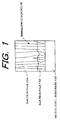
- FIG. 1 illustrating schematically a thin film structure, such a manner that, for example, a 6H-SiC (0001) substrate being a type of SiC substrate is used, an AlN thin film is formed thereon (in a thickness of, for example, 10 nm or thicker), and a GaN system thin film is further formed thereon (in a thickness of, for example, 1.5 ⁇ m) has been applied heretofore.
- a 6H-SiC (0001) substrate being a type of SiC substrate is used, an AlN thin film is formed thereon (in a thickness of, for example, 10 nm or thicker), and a GaN system thin film is further formed thereon (in a thickness of, for example, 1.5 ⁇ m) has been applied heretofore.
- an AlN thin film has 1% of a rate of lattice mismatch with an SiC substrate, and on one hand, it exhibits a rate of lattice mismatch of 2.5% with a GaN thin film, such AlN thin film has been used as a buffer layer between the SiC substrate and the GaN system thin film.
- threading dislocations appear in the first GaN layer 204 at a dislocation density of 10 9 to 10 10 cm -2 order, while GaN crystal grown from the first GaN layer 204 which has not been covered by the mask 206 comes to grow laterally (directions indicated by the arrows in FIG. 2(b)) on the mask 206, so that a dislocation density of threading dislocations in the second GaN layer 208 was reduced to 10 7 cm -2 order.
- the present invention has been made in view of various problems involved in the prior art as described above, and an object of the invention is to provide a method for the formation of a semiconductor layer (layers) by which a defect density of structural defects, particularly a dislocation density of threading dislocations in the resulting semiconductor layer(s) can be remarkably reduced, so that hours of work can be shortened as well as a manufacturing cost can be reduced without requiring any complicated process in case of forming a semiconductor layer (layers) of, for example, a GaN (gallium nitride) or the like thin, thick or the like film(s) on a substrate or the like made of a variety of materials.
- a semiconductor layer (layers) of, for example, a GaN (gallium nitride) or the like thin, thick or the like film(s) on a substrate or the like made of a variety of materials.
- a method for the formation of a semiconductor layer for forming the semiconductor layer comprises supplying a structural defect suppressing material for suppressing structural defects in the semiconductor layer.
- a structural defect suppressing material for suppressing structural defects in a semiconductor is supplied, such structural defect suppressing material is adsorbed or applied at a position where a structural defect, and particularly threading dislocation appears on a surface of a material layer on which is to be formed the semiconductor layer, so that structural defects, particularly threading dislocations in the semiconductor layer are suppressed, whereby a dislocation density can be significantly reduced.
- a method for the formation of a semiconductor layer for forming the semiconductor layer comprises supplying a structural defect suppressing material for suppressing structural defects in the semiconductor layer onto a surface of the layer of a material from which the semiconductor layer is to be formed.
- the structural defect suppressing material for suppressing structural defects in a semiconductor is supplied onto a surface of the layer of a material from which the semiconductor layer is to be formed, the structural defect suppressing material is adsorbed or applied at a position where a structural defect, and particularly threading dislocation appears on a surface of the layer of a material on which is to be formed the semiconductor layer, so that structural defects, particularly threading dislocations in the semiconductor layer are suppressed, whereby a dislocation density can be significantly reduced.
- a method for the formation of a semiconductor layer for forming the semiconductor layer comprises supplying simultaneously a structural defect suppressing material for suppressing structural defects in the semiconductor layer with a material from which the semiconductor layer is to be formed in case of forming the semiconductor layer.
- the structural defect suppressing material for suppressing structural defects in a semiconductor is supplied simultaneously with a material from which the semiconductor layer is to be formed, the structural defect suppressing material is adsorbed or applied at a position where a structural defect, and particularly threading dislocation appears on a surface of the layer of a material on which is to be formed the semiconductor layer, so that structural defects, particularly threading dislocations in the semiconductor layer are suppressed, whereby a dislocation density can be significantly reduced.
- a method for the formation of a semiconductor layer for forming the semiconductor layer comprises a first step for forming a buffer layer on a substrate; a second step for supplying a predetermined amount of a structural defect suppressing material for suppressing structural defects in the semiconductor layer to be formed on a surface of the buffer layer formed in the first step; a third step for forming the semiconductor layer on a surface of the buffer layer in which said structural defect suppressing material has been supplied onto the semiconductor layer to be formed in the second step; and a film thickness of the semiconductor layer in the third step being made to be 1 nm or thicker.
- a buffer layer is formed on a substrate in the first step, a predetermined amount of a structural defect suppressing material for suppressing structural defects in the semiconductor layer to be formed is supplied on a surface of the buffer layer in the second step, and the semiconductor layer is formed on a surface of the buffer layer onto which has been supplied the structural defect suppressing material in the third step in a film thickness of 1 nm or thicker, so that structural defects, particularly a density of threading dislocations can be significantly reduced in semiconductor layer formed by the structural defect suppressing material which has been supplied on the buffer layer with a predetermined amount so as to have a film thickness of 1 nm or thicker, while a number of structural defects, particularly threading dislocations appear in a buffer layer formed on a substrate.
- the method for the formation of a semiconductor layer described in the immediately above paragraph may be arranged to further comprises a fourth step for supplying a predetermined amount of a structural defect suppressing material for suppressing structural defects in the semiconductor layer to be formed onto a surface of the semiconductor layer formed in the third step; a fifth step for forming the semiconductor layer on a surface of the semiconductor layer in which the structural defect suppressing material has been supplied onto the semiconductor layer to be formed in the fourth step; and implementing one or more times of the fourth step and the fifth step after finishing the third step.
- the method for the formation of a semiconductor layer described in the above paragraph may be arranged in such that at least any of laser beam, electron beam, radical beam, ion beam, or atomic hydrogen is applied in at least either of the second step and the fourth step.
- the method for the formation of a semiconductor layer described in the above paragraph may be arranged in such that a predetermined amount of plural types of structural defect suppressing materials for suppressing structural defects in the semiconductor layer to be formed are supplied in at least either of the second step and the fourth step.
- a method for the formation of a semiconductor layer for forming the semiconductor layer comprises a first step for forming a buffer layer on a substrate; a second step for starting a supply of a material for forming the semiconductor layer to be formed as well as a supply of a structural defect suppressing material for suppressing structural defects in the semiconductor layer to be formed onto a surface of the buffer layer formed in the first step at the same timing, besides finishing the supply of a structural defect suppressing material for suppressing structural defects in the semiconductor layer to be formed at a timing prior to that of the supply of a material for forming the semiconductor layer to be formed; and a film thickness of the semiconductor layer in the second step being made to be 1 nm or thicker.
- a buffer layer is formed on a substrate in the first step; a supply of a material for forming the semiconductor layer to be formed as well as a supply of a structural defect suppressing material for suppressing structural defects in the semiconductor layer to be formed onto a surface of the buffer layer are started at the same timing, besides the supply of a structural defect suppressing material for suppressing structural defects in the semiconductor layer to be formed is finished at a timing prior to that of the supply of a material for forming the semiconductor layer to be formed in the second step; and the semiconductor layer is formed in a film thickness of 1 nm or thicker, so that structural defects, particularly a density of threading dislocations can be significantly reduced in semiconductor layer formed by the structural defect suppressing material which has been supplied on the buffer layer with a predetermined amount so as to have a film thickness of 1 nm or thicker, while a number of structural defects, particularly threading dislocations appear in a buffer layer formed on a substrate.
- a method for the formation of a semiconductor layer described in the immediately above paragraph may be arranged to further comprises a third step for starting a supply of a material for forming a semiconductor layer to be formed as well as a supply of a structural defect suppressing material for suppressing structural defects in the semiconductor layer to be formed onto a surface of the above described semiconductor layer formed in the second step at the same timing, besides finishing the supply of a structural defect suppressing material for suppressing structural defects in the semiconductor layer to be formed at a timing prior to that of the supply of a material for forming the semiconductor layer to be formed; and implementing at least one time of the third step after finishing the second step.
- a supply of a material for forming a semiconductor layer to be formed as well as a supply of a structural defect suppressing material for suppressing structural defects in the semiconductor layer to be formed onto a surface of the above described semiconductor layer formed in the second step are started at the same timing, besides the supply of a structural defect suppressing material for suppressing structural defects in the semiconductor layer to be formed is finished at a timing prior to that of the supply of a material for forming the semiconductor layer to be formed in the third step; and at least one time of the third step is implemented after finishing the second step, whereby a plurality of semiconductor layers can be laminated.
- a method for the formation of a semiconductor layer described in the above paragraph may be arranged in such that at least any of laser beam, electron beam, radical beam, ion beam, or atomic hydrogen is applied in at least either of the second step and the third step.
- a method for the formation of a semiconductor layer described in the above paragraph may be arranged in such that a predetermined amount of plural types of structural defect suppressing materials for suppressing structural defects in the semiconductor layer to be formed are supplied in at least either of the second step and the third step.
- the above described substrate may be a silicon carbide substrate (6H-SiC substrate, 4H-SiC substrate), a laminated substrate of silicon carbide and silicon (SiC/Si substrate), a silicon substrate (Si substrate), a sapphire substrate (Al 2 O 3 substrate), a laminated substrate of zinc oxide and sapphire (ZnO/Al 2 O 3 substrate), a germanium substrate (Ge substrate), a gallium arsenide substrate (GaAs substrate), an indium arsenide substrate (InAs substrate), a gallium phosphide substrate (GaP substrate), an indium phosphide substrate (InP substrate), or a spinel substrate (MgAl 2 O 3 , LiGaO 2 );
- the above described structural defect suppressing material may be H (hydrogen) of the group I-A; Be (beryllium), or Mg (magnesium) of the group II-A; Al (
- a method for the formation of semiconductor layers on a substrate through a buffer layer comprises applying an MOCVD (Metalorganic Chemical Vapor Deposition), an MBE (Molecular Beam Epitaxy), a CBE (Chemical Beam Epitaxy), an HAVPE (Halide Vapor Phase Epitaxy), a GSMBE (Gas-Source Molecular Beam Epitaxy), an MOMBE (Metalorganic MBE), an LPE (Liquid Phase Epitaxy), a CVD (Chemical Vapor Deposition), a sputtering, or a vacuum deposition process; a first step for supplying solid gallium (Ga), trimethylgallium (TMG), or triethylgallium (TEG), solid aluminum (Al), trimethylaluminum (TMA), triethylaluminum (TEA), trimethylaminealum (TMAAl), dimethylethylaminealum (DMEAAl), or triisobutyla
- MOCVD Metalorgan
- an MOCVD Metalorganic Chemical Vapor Deposition
- an MBE Molecular Beam Epitaxy
- CBE Chemical Beam Epitaxy
- an HAVPE Halide Vapor Phase Epitaxy
- GSMBE Gas-Source Molecular Beam Epitaxy
- MOMBE Metalorganic MBE
- LPE Liquid Phase Epitaxy
- CVD Chemical Vapor Deposition
- TMAA trimethylgallium
- TMA triethylaluminum
- TMAA triethylaluminum
- TMAAl trimethylaminealum
- DMEAAl dimethylethylaminealum
- TI triisobutylaluminum
- Si is adsorbed on the surface of a GaN layer, an AlN layer, or an AlGaN layer, whereby the surface of the GaN layer, the AlN layer, or the AlGaN layer is reformed in atomic level, and thereafter another GaN layer, AlN layer, or AlGaN layer is formed as a semiconductor layer, so that a defect density of structural defects, particularly a dislocation density of threading dislocations in the GaN layer, the AlN layer, or the AlGaN layer being the semiconductor layer can be significantly reduced.
- Si supplied as a structural defect suppressing material is a metal used as an n-type impurity material for a GaN layer, an AlN layer, or an AlGaN layer, it does not affect adversely quality of the resulting semiconductor layer in case of forming the GaN layer, the AlN layer, or the AlGaN layer as an n-type semiconductor layer, and thus, such Si can be easily supplied.
- a method for the formation of a semiconductor layer in which a GaN layer or an AlGaN layer is formed on an SiC substrate or an Al 2 O 3 substrate by means of MOCVD (Metalorganic Chemical Vapor Deposition) equipment comprises a first step for either supplying trimethylgallium (TMG) or triethylgallium (TEG) and ammonia (NH 3 ) onto a surface of the SiC substrate or the Al 2 O 3 substrate to form a GaN layer as a buffer layer, or supplying trimethylgallium (TMG) or triethylgallium (TEG) and trimethylaluminum (TMA) or triethylaluminum (TEA) and ammonia (NH 3 ) thereon to form an AlGaN layer as a buffer layer; a second step for supplying Si being an n-type impurity material used for a GaN layer or an AlGaN layer on a surface of the GaN layer or the AlG
- MOCVD Metalorganic
- a method for the formation of a semiconductor layer in which a GaN layer or an AlGaN layer is formed on an SiC substrate or an Al 2 O 3 substrate by means of MOCVD (Metalorganic Chemical Vapor Deposition) equipment either trimethylgallium (TMG) or triethylgallium (TEG) and ammonia (NH 3 ) are supplied onto a surface of the SiC substrate or the Al 2 O 3 substrate to form a GaN layer as a buffer layer, or trimethylgallium (TMG) or triethylgallium (TEG) and trimethylaluminum (TMA) or triethylaluminum (TEA) and ammonia (NH 3 ) are supplied thereon to form an AlGaN layer as a buffer layer in the first step; Si being an n-type impurity material used for a GaN layer or an AlGaN layer is supplied on a surface of the GaN layer or the AlGaN layer being the buffer
- Si in the silane (SiH 4 ), disilane (Si 2 H 6 ), or tetraethylsilane (TESi) is adsorbed on a surface of a GaN layer, or an AlGaN layer, whereby the surface of the GaN layer, or the AlGaN layer is reformed in atomic level, and thereafter another GaN layer, or AlGaN layer is formed as a semiconductor layer, so that a defect density of structural defects, particularly a dislocation density of threading dislocations in the GaN layer being a semiconductor layer can be significantly reduced.
- Si supplied as a structural defect suppressing material is a metal used as an n-type impurity material for a GaN layer, or an AlGaN layer, it does not affect adversely quality of the resulting semiconductor layer in case of forming the GaN layer, or the AlGaN layer as a semiconductor layer, and thus, such Si can be easily supplied.
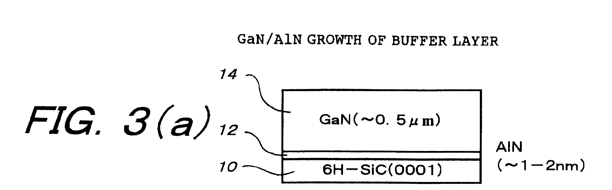
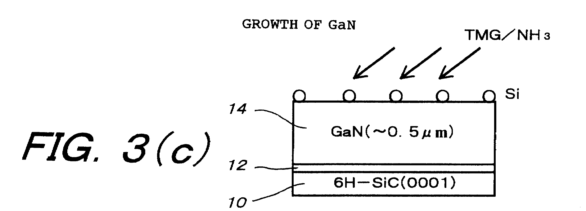
- FIG. 3 illustrates schematically a state in which a GaN thin film is formed as a semiconductor layer on a 6H-SiC (0001) substrate being a type of SiC (silicon carbide) substrates in time-series order in accordance with the first embodiment of a method for the formation of a semiconductor layer according to the present invention wherein the state illustrated in FIG. 3(a) shifts successively to the state illustrated in FIG. 3(b), the state illustrated in FIG. 3(c), and the state illustrated in FIG. 3(d).
- MOCVD metalorganic chemical vapor deposition
- FIGS. 4(a) through 4(d) indicate treating conditions in case of forming the thin film structure illustrated in FIG. 3(d) in accordance with MOCVD process
- FIG. 5 is an explanatory diagram showing a timing for supplying TESi (which is mentioned hereunder) and gases for forming a GaN thin film as a semiconductor layer in accordance with the first embodiment of a method for the formation of a semiconductor layer according to the present invention.
- FIG. 6 is an electron micrograph taken by means of a transmission type electron microscope (TEM) showing a section of the thin film structure illustrated in FIG. 3(d) which is formed in accordance with the treating conditions indicated in FIGS. 4(a), 4(b), 4(c), and 4(d).
- TEM transmission type electron microscope
- an outline of a treatment in case of forming the thin film structure illustrated in FIG. 3(d) in accordance with the first embodiment of a method for the formation of a semiconductor layer according to the present invention will be described herein.
- an AlN (aluminum nitride) thin film 12 is formed as a buffer layer on a 6H-SiC (0001) substrate 10 as a substrate (see FIG. 3(a)).
- a GaN buffer layer 14 is formed on the AlN thin film 12 as a buffer layer , and tetraethylsilane (TESi) is supplied on a surface 14a of the GaN buffer layer 14 as an n-type impurity material (see FIG. 3(b)).
- TESi tetraethylsilane
- TMG trimethylgallium
- NH 3 ammonia
- the TESi functions to suppress structural defects, particularly growth of threading dislocations, whereby structural defects, particularly a dislocation density of the GaN layer 18 which is formed as a semiconductor layer by supplying trimethylgallium (TMG) and ammonia (NH 3 ) after the supply of TESi as a result of crystal growth of GaN could be remarkably reduced.
- TMG trimethylgallium
- NH 3 ammonia
- an AlN thin film 12 being a buffer layer is formed on a 6H-SiC (0001) substrate 10 in accordance with the treating condition indicated in FIG. 4(a), and further, a GaN buffer layer 14 being a buffer layer is formed on the AlN thin film 12 in accordance with the treating condition indicated in FIG. 4(b) (see FIG. 3(a)).
- the GaN buffer layer 14 is a buffer layer interposed between the AlN thin film 12 formed under the GaN buffer layer 14 and the AlN thin film 12 formed on the GaN buffer layer 14, and threading dislocations with a dislocation density in the order of 10 9 to 10 10 cm -2 are observed in the GaN buffer layer 14 due to lattice mismatch with respect to the substrate material (6H-SiC (0001)) (see FIG. 5).
- TESi a metal used as an n-type impurity material with respect to GaN
- TESi a metal used as an n-type impurity material with respect to GaN
- threading locations appear in the GaN buffer layer 14 as described above, and in this respect, an atomic clearance expands at a position where the threading dislocations appear on the surface 14a of the GaN buffer layer 14.
- dislocation core position a magnitude of expansion in an atomic clearance at a position where the threading locations appear (hereinafter referred to as "dislocation core position") on the surface 14a of the GaN buffer layer 14 as described above is 8. fold in dislocation core structure according to literature, it may be considered that such dimension is the one wherein Si in the TESi supplied can be easily adsorbed thereat (can be combined therewith).
- T3 a timing T3 (see FIG. 5) when a predetermined period of time t2 (see FIG. 5) elapsed from the timing T2 (see FIG. 5), a supply of trimethylgallium (TMG) and ammonia (NH 3 ) is finished.
- TMG trimethylgallium
- NH 3 ammonia
- TESi being a structural defect suppressing material
- a surface 14a of a GaN buffer layer 14 being a buffer layer is reformed in an atomic level by means of Si in the TESi, whereby a defect density of structural defects, particularly a dislocation density of threading dislocations in a GaN layer 18 being a semiconductor layer can be significantly reduced.
- Si in TESi being a structural defect suppressing material is adsorbed on the surface 14a of the GaN buffer layer 14 to reform the surface 14a of the GaN buffer layer 14 in an atomic level, and then, the GaN layer 18 is formed in the first embodiment of a method for the formation of a semiconductor layer according to the present invention. Therefore, no portion such as boundary portions (the portions dotted in FIG. 2(b)) where threading locations produced in ELO process appear easily exists in the GaN layer 18, so that a GaN thin film which is easily utilized in industry can be obtained, because a field of GaN thin film which can be applied to a device and the like is not restricted.
- a defect density of structural defects, particularly a dislocation density of threading dislocations in the GaN layer 18 (see FIG. 3(d)) formed in accordance with the treating conditions indicated in FIGS. 4(a) to 4(d) is remarkably reduced.
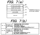
- TESi being a metal used as a n-type impurity material with respect to GaN is supplied to a surface of the GaN layer 18 at a timing T1 (see FIG. 5) in accordance with a treating condition indicated in FIG. 7(b-1).
- TESi being a structural defect suppressing material described above as in the case of the GaN layer 18.
- a supply of a structural defect suppressing material (TESi) as well as a supply of trimethylgallium (TMG) and ammonia (NH 3 ) are repeated on the surface of a semiconductor layer (GaN layer 18) formed, whereby a plurality of layers of the GaN layer 18 and the GaN layer 20 being semiconductor layers can be laminated.
- TESi structural defect suppressing material
- TMG trimethylgallium
- NH 3 ammonia
- FIGS. 8(a-1) and 8(a-2) illustrate schematically each state wherein a GaN thin film (films) as a semiconductor layer (layers) is (are) formed in a time-series order in accordance with the third embodiment of a method for the formation of a semiconductor layer (layers) of the present invention.
- the state shown in FIG. 8(a-1) shifts to the state shown in FIG. 8(b-2).
- FIG. 8(b) a treating condition in case of forming a thin film structure shown in FIG. 8(a-2) in accordance with MOCVD process is indicated in FIG. 8(b).
- TESi is supplied on the surface 14a of the GaN buffer layer 14 in the above describe first embodiment of a method for the formation of a semiconductor layer of the present invention (see FIG. 3(b) and FIG. 4(c)), while TESi is supplied on the surface 14a of the GaN buffer layer 14 as well as light beam is also supplied thereon in the third embodiment of a method for the formation of semiconductor layers of the invention.
- TESi is supplied on the surface 14a of the GaN buffer layer 14 being a buffer layer formed as in the case of the first embodiment of a method for the formation of a semiconductor layer of the present invention as well as light beam is applied from a mercury lamp thereon.
- TESi is supplied (see FIG. 8(a-1)) on a surface of the GaN buffer layer 14 (see FIG. 3(a)) formed in accordance with the treating conditions indicated in FIGS. 4(a) and 4(b) at a timing T1 (see FIG. 5) in accordance with the treating condition indicated in FIG. 8(b).
- Si in TESi is easily adsorbed at a dislocation core position on the surface 14a of the GaN buffer layer 14, so that reforming of the surface 14a of the GaN buffer layer 14 in atomic level is more promoted.
- a supply of TESi onto the surface 14a of the GaN buffer layer 14 is finished, and at the same time, a supply of trimethylgallium (TMG) and ammonia (NH 3 ) is started in accordance with a treating condition indicated in FIG. 4(d) to form a GaN layer 18 through an interface (see FIG. 8(a-2)) treated by supplying the TESi on the GaN buffer layer 14 under application of light beam from mercury lamp (see FIG. 8(a-2)).
- TMG trimethylgallium
- NH 3 ammonia
- TESi being a structural defect suppressing material as described above.
- a defect density of structural defects, particularly a dislocation density of threading dislocations in the GaN layer 18 being a semiconductor layer can be remarkably reduced by the supply of TESi being a structural defect suppressing material, besides as a result of application of light beam by means of a mercury lamp in addition to the supply of TESi being a structural defect suppressing material, surface diffusion of Si in the TESi is promoted on the surface 14a of the GaN buffer layer 14, so that Si in the TESi is easily adsorbed at a dislocation core position on the surface 14a of the GaN buffer layer 14, whereby reforming of the surface 14a of the GaN buffer layer 14 can be more promoted in an atomic level.
- FIGS. 9(a) and 9(b) a fourth embodiment of a method for the formation of semiconductor layers according to the present invention will be described by referring to FIGS. 9(a) and 9(b).
- FIGS. 9(a-1) and 9(a-2) illustrate schematically each state wherein a GaN thin film (films) as a semiconductor layer (layers) is (are) formed in a time-series order in accordance with the fourth embodiment of a method for the formation of a semiconductor layer (layers) of the present invention.
- the state shown in FIG. 9(a-1) shifts to the state shown in FIG. 9(b-2).
- FIG. 9(b) a treating condition in case of forming a thin film structure shown in FIG. 9(a-2) in accordance with MOCVD process is indicated in FIG. 9(b).
- TESi is supplied on the surface 14a of the GaN buffer layer 14 in the above described first embodiment of a method for the formation of a semiconductor layer of the present invention (see FIG. 3(b) and FIG. 4(c)), while TESi is supplied together with other types of structural defect suppressing material on the surface 14a of the GaN buffer layer 14 in the fourth embodiment of a method for the formation of semiconductor layers of the present invention.
- TESi is supplied on the surface of a GaN buffer layer 14 being a buffer layer formed similarly as in the first embodiment of a method for the formation of a semiconductor layer according to the present invention as well as TMIn is also supplied thereon.
- TESi is supplied (see FIG. 7(a-1)) on a surface of the GaN buffer layer 14 (see FIG. 3(a)) formed in accordance with the treating conditions indicated in FIGS. 4(a) and 4(b) at a timing T1 (see FIG. 5) according to the treating condition indicated in FIG. 9(b).
- TMIn is supplied on the surface 14a of the GaN buffer layer 14 together with a supply of TESi, so that surface diffusion of Si in TESi on the surface 14a of the GaN buffer layer 14 is promoted as a result of supplying In in the TMIn.
- Si in TESi is easily adsorbed at a dislocation core position on the surface 14a of the GaN buffer layer 14, so that reforming of the surface 14a of the GaN buffer layer 14 in atomic level is more promoted.
- a supply of TESi onto the surface 14a of the GaN buffer layer 14 is finished, and at the same time, a supply of trimethylgallium (TMG) and ammonia (NH 3 ) is started in accordance with a treating condition indicated in FIG. 4(d) to form a GaN layer 18 through an interface (see FIG. 9(a-2)) treated by supplying the TESi together with the TMIn on the GaN buffer layer 14 (see FIG. 7(a-2)).
- TMG trimethylgallium
- NH 3 ammonia
- TESi being a structural defect suppressing material as described above.
- a defect density of structural defects, particularly a dislocation density of threading dislocations in the GaN layer 18 being a semiconductor layer is remarkably reduced by the supply of TESi being a structural defect suppressing material, besides as a result of supplying TMIn in addition to the supply of TESi being a structural defect suppressing material, surface diffusion of Si in the TESi is promoted on the surface 14a of the GaN buffer layer 14, so that Si in the TESi is easily adsorbed at a dislocation core position on the surface 14a of the GaN buffer layer 14, whereby reforming of the surface 14a of the GaN buffer layer 14 can be more promoted in an atomic level.
- FIGS. 10(a) and 10(b) a fifth embodiment of a method for the formation of semiconductor layers according to the present invention will be described by referring to FIGS. 10(a) and 10(b).
- FIG. 10(a) is an explanatory diagram showing a timing for supplying TESi as well as a timing for supplying gases for forming a GaN thin film as a semiconductor layer in accordance with the fifth embodiment of a method for the formation of semiconductor layers of the present invention
- FIG. 10(b) illustrates schematically a state wherein a GaN thin film as a semiconductor layer in accordance with the fifth embodiment of a method for the formation of semiconductor layers of the invention.
- a supply of TESi is made at a different timing from that of a supply of trimethylgallium (TMG) and ammonia (NH 3 ) for forming a GaN layer 18 in the first embodiment of a method for the formation of semiconductor layers of the invention (see FIG. 5), while a supply of TESi is made at the same timing as that of a supply of trimethylgallium (TMG) and ammonia (NH 3 ) for forming a GaN layer 18 in the fifth embodiment of a method for the formation of semiconductor layers of the invention.
- TMG trimethylgallium
- NH 3 ammonia
- a start of supplying TESi (see the timing T1 in FIG. 5) is different in timing from that of supplying trimethylgallium (TMG) and ammonia (NH 3 ) for forming the GaN layer 18 (see the timing T2 in FIG. 5) as described above in the first embodiment of a method for the formation of a semiconductor layer of the invention, so that there is no case where TESi being a structural defect suppressing material as well as trimethylgallium (TMG) and ammonia (NH 3 ) for forming the GaN layer 18 are supplied at the same timing.
- TMG trimethylgallium
- NH 3 ammonia
- a supply of TESi onto a surface 14a of the GaN buffer layer 14 is started at a timing T1 (see FIG. 10(a)) in accordance with the treating condition indicated in FIG. 4(c), and at the same time, a supply of trimethylgallium (TMG) and ammonia (NH 3 ) for forming the GaN layer 18 is started according to the treating condition indicated in FIG. 4(d).
- T1 trimethylgallium
- NH 3 ammonia
- a supply of TESi onto the surface 14a of the GaN buffer layer 14 is finished.
- a supply of trimethylgallium (TMG) and ammonia (NH 3 ) for forming the GaN layer 18 is finished.
- TESi as well as trimethylgallium (TMG) and ammonia (NH 3 ) for forming the GaN layer 18 are supplied on the surface 14a of the GaN buffer layer 14 at the same timing.
- TMG trimethylgallium
- NH 3 ammonia
- both TESi as well as trimethylgallium (TMG) and ammonia (NH 3 ) for forming the GaN layer 18 are supplied during a predetermined period of time tl extending from the timing T1 to the timing T2, so that a TESi supply layer 16 containing TESi is formed.
- TMG trimethylgallium
- NH 3 ammonia
- TESi being a structural defect suppressing material as described above.
- a defect density of structural defects, particularly a dislocation density of threading dislocations in the GaN layer 18 being a semiconductor layer can be remarkably reduced by a simultaneous supply of TESi being a structural defect suppressing material with trimethylgallium (TMG) and ammonia (NH 3 ) for forming the GaN layer 18 being a semiconductor layer.
- TMG trimethylgallium
- NH 3 ammonia
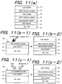
- FIG. 11(a) a sixth embodiment of a method for the formation of semiconductor layers according to the present invention will be described by referring to FIG. 11(a).
- FIG. 11(a) illustrates schematically a state wherein GaN thin films are formed as semiconductor layers in accordance with the sixth embodiment of a method for the formation of semiconductor layers of the invention.
- a supply of TESi at a timing T1 (see FIG. 10(a)) in accordance with the treating condition indicated in FIG. 7(b-1), and at the same time, a supply of trimethylgallium (TMG) and ammonia (NH 3 ) for forming a GaN layer 18' is started according to the treating condition indicated in FIG. 7(b-2).
- T1 trimethylgallium
- NH 3 ammonia
- a supply of TESi onto the surface 14a of the GaN buffer layer 14 is finished.
- a supply of trimethylgallium (TMG) and ammonia (NH 3 ) for forming the GaN layer 18' is finished.
- a TESi supply layer 16' is formed on the surface of the GaN layer 18, and the GaN layer 18' is formed on a surface of the TESi supply layer 16' (see FIG. 11(a)).
- TESi being a structural defect suppressing material as described above.
- a supply of a structural defect suppressing material (TESi) as well as a supply of trimethylgallium (TMG) and ammonia (NH 3 ) are repeated on the surface of a semiconductor layer (GaN layer 18) formed, whereby a plurality of layers of the GaN layer 18 and the GaN layer 18' being semiconductor layers can be laminated.
- TESi structural defect suppressing material
- TMG trimethylgallium
- NH 3 ammonia
- FIG. 11(b) A seventh embodiment of a method for the formation of semiconductor layers according to the present invention will be described hereinafter by referring to FIG. 11(b).
- TESi as well as trimethylgallium (TMG) and ammonia (NH 3 ) for forming the GaN layer 18 are supplied on a surface 14a of a GaN buffer layer 14 being a buffer layer formed as in the case of the first embodiment of a method for the formation of a semiconductor layer of the present invention, besides light beam is applied from a mercury lamp thereon.
- TMG trimethylgallium
- NH 3 ammonia
- a supply of TESi onto the surface of the GaN buffer layer 14 is started at a timing T1 (see FIG. 10(a)) in accordance with the treating condition indicated in FIG. 8(b), and at the same time, a supply of trimethylgallium (TMG) and ammonia (NH 3 ) for forming the GaN layer 18 is started according to the treating condition indicated in FIG. 4(d).
- T1 trimethylgallium
- NH 3 ammonia
- Si in TESi is easily adsorbed at a dislocation core position on the surface 14a of the GaN buffer layer 14, so that reforming of the surface 14a of the GaN buffer layer 14 is more promoted in atomic level.
- a supply of TESi onto the surface 14a of the GaN buffer layer 14 is finished.
- TMG trimethylgallium
- NH 3 ammonia
- TESi being a structural defect suppressing material as described above.
- a defect density of structural defects, particularly a dislocation density of threading dislocations in the GaN layer 18 being a semiconductor layer can be remarkably reduced by the simultaneous supply of TESi being a structural defect suppressing material with trimethylgallium (TMG) and ammonia (NH 3 ) for forming the GaN layer 18, besides as a result of application of light beam by means of a mercury lamp in addition to the simultaneous supply of TESi being a structural defect suppressing material with trimethylgallium (TMG) and ammonia (NH 3 ) for forming the GaN layer 18, surface diffusion of Si in the TESi is promoted on the surface 14a of the GaN buffer layer 14, so that Si in the TESi is easily adsorbed at a dislocation core position on the surface 14a of the GaN buffer layer 14, whereby reforming of the surface 14a of the GaN buffer layer 14 can be more promoted in an atomic level.
- TMG trimethylgallium
- NH 3 ammonia
- FIG. 11(c) a eighth embodiment of a method for the formation of semiconductor layers according to the present invention will be described by referring to FIG. 11(c).
- TESi as well as trimethylgallium (TMG) and ammonia (NH 3 ) for forming a GaN layer 18 are supplied on the surface 14a of a GaN buffer layer 14 being a buffer layer formed similarly as in the first embodiment of a method for the formation of a semiconductor layer according to the present invention, besides TMIn is also supplied thereon.
- TMG trimethylgallium
- NH 3 ammonia
- Si in TESi is easily adsorbed at a dislocation core position on the surface 14a of the GaN buffer layer 14, so that reforming of the surface 14a of the GaN buffer layer 14 is more promoted in atomic level.
- a supply of TESi and TMIn onto the surface 14a of the GaN buffer layer 14 is finished.
- TMG trimethylgallium
- NH 3 ammonia
- TESi being a structural defect suppressing material as described above.
- a defect density of structural defects, particularly a dislocation density of threading dislocations in the GaN layer 18 being a semiconductor layer can be remarkably reduced by the simultaneous supply of TESi being a structural defect suppressing material with trimethylgallium (TMG) and ammonia (NH 3 ) for forming the GaN layer 18, besides as a result of supplying TMIn in addition to the simultaneous supply of TESi being a structural defect suppressing material with trimethylgallium (TMG) and ammonia (NH 3 ) for forming the GaN layer 18, surface diffusion of Si in the TESi is promoted on the surface 14a of the GaN buffer layer 14, so that Si in the TESi is easily adsorbed at a dislocation core position on the surface 14a of the GaN buffer layer 14, whereby reforming of the surface 14a of the GaN buffer layer 14 can be more promoted in an atomic level.
- TMG trimethylgallium
- NH 3 ammonia
- the present invention has been constituted as mentioned above, such excellent advantages that a defect density of structural defects, particularly a dislocation density of threading dislocations in the resulting semiconductor layer can be remarkably reduced, so that reduction of hours of work can be realized as well as that a manufacturing cost can be reduced without requiring any complicated process in case of forming a thin or thick film semiconductor layer (layers) made of GaN or the like on a substrate made of a variety of materials are achieved.
Landscapes
- Chemical & Material Sciences (AREA)
- Metallurgy (AREA)
- Engineering & Computer Science (AREA)
- Crystallography & Structural Chemistry (AREA)
- Materials Engineering (AREA)
- Organic Chemistry (AREA)
- Inorganic Chemistry (AREA)
- General Chemical & Material Sciences (AREA)
- Chemical Kinetics & Catalysis (AREA)
- Led Devices (AREA)
- Physical Deposition Of Substances That Are Components Of Semiconductor Devices (AREA)
- Semiconductor Lasers (AREA)
- Recrystallisation Techniques (AREA)
Abstract

Description
Claims (22)
- A method for the formation of a semiconductor layer for forming the semiconductor layer comprising:
supplying a structural defect suppressing material for suppressing structural defects in the semiconductor layer. - A method for the formation of a semiconductor layer for forming the semiconductor layer comprising:
supplying a structural defect suppressing material for suppressing structural defects in the semiconductor layer onto a surface of the layer of a material from which the semiconductor layer is to be formed. - A method for the formation of a semiconductor layer for forming the semiconductor layer comprising:
supplying simultaneously a structural defect suppressing material for suppressing structural defects in the semiconductor layer with a material from which the semiconductor layer is to be formed in case of forming the semiconductor layer. - A method for the formation of a semiconductor layer for forming the semiconductor layer comprising:a first step for forming a buffer layer on a substrate;a second step for supplying a predetermined amount of a structural defect suppressing material for suppressing structural defects in the semiconductor layer to be formed on a surface of said buffer layer formed in said first step;a third step for forming the semiconductor layer on a surface of said buffer layer in which said structural defect suppressing material has been supplied onto said semiconductor layer to be formed in said second step; anda film thickness of said semiconductor layer in said third step being made to be 1 nm or thicker.
- A method for the formation of a semiconductor layer as claimed in claim 4 comprising further:a fourth step for supplying a predetermined amount of a structural defect suppressing material for suppressing structural defects in the semiconductor layer to be formed onto a surface of said semiconductor layer formed in said third step;a fifth step for forming said semiconductor layer on a surface of said semiconductor layer in which said structural defect suppressing material has been supplied onto said semiconductor layer to be formed in said fourth step; andimplementing one or more times of said fourth step and said fifth step after finishing said third step.
- A method for the formation of a semiconductor layer as claimed in claim 4 wherein:
at least any of laser beam, electron beam, radical beam, ion beam, or atomic hydrogen is applied in at least either of said second step and said fourth step. - A method for the formation of a semiconductor layer as claimed in claim 5 wherein:
at least any of laser beam, electron beam, radical beam, ion beam, or atomic hydrogen is applied in at least either of said second step and said fourth step. - A method for the formation of a semiconductor layer as claimed in claim 4 wherein:
a predetermined amount of plural types of structural defect suppressing materials for suppressing structural defects in the semiconductor layer to be formed are supplied in at least either of said second step and said fourth step. - A method for the formation of a semiconductor layer as claimed in claim 5 wherein:
a predetermined amount of plural types of structural defect suppressing materials for suppressing structural defects in the semiconductor layer to be formed are supplied in at least either of said second step and said fourth step. - A method for the formation of a semiconductor layer as claimed in claim 6 wherein:
a predetermined amount of plural types of structural defect suppressing materials for suppressing structural defects in the semiconductor layer to be formed are supplied in at least either of said second step and said fourth step. - A method for the formation of a semiconductor layer as claimed in claim 7 wherein:
a predetermined amount of plural types of structural defect suppressing materials for suppressing structural defects in the semiconductor layer to be formed are supplied in at least either of said second step and said fourth step. - A method for the formation of a semiconductor layer for forming the semiconductor layer comprising:a first step for forming a buffer layer on a substrate;a second step for starting a supply of a material for forming the semiconductor layer to be formed as well as a supply of a structural defect suppressing material for suppressing structural defects in the semiconductor layer to be formed onto a surface of said buffer layer formed in said first step at the same timing, besides finishing said supply of a structural defect suppressing material for suppressing structural defects in the semiconductor layer to be formed at a timing prior to that of said supply of a material for forming the semiconductor layer to be formed; anda film thickness of said semiconductor layer in said second step being made to be 1 nm or thicker.
- A method for the formation of a semiconductor layer as claimed in claim 12 comprising further;a third step for starting a supply of a material for forming a semiconductor layer to be formed as well as a supply of a structural defect suppressing material for suppressing structural defects in the semiconductor layer to be formed onto a surface of said buffer layer formed in said second step at the same timing, besides finishing said supply of a structural defect suppressing material for suppressing structural defects in the semiconductor layer to be formed at a timing prior to that of said supply of a material for forming the semiconductor layer to be formed; andimplementing at least one time of said third step after finishing said second step.
- A method for the formation of a semiconductor layer as claimed in claim 12 wherein:
at least any of laser beam, electron beam, radical beam, ion beam, or atomic hydrogen is applied in at least either of said second step and said third step. - A method for the formation of a semiconductor layer as claimed in claim 13 wherein:
at least any of laser beam, electron beam, radical beam, ion beam, or atomic hydrogen is applied in at least either of said second step and said third step. - A method for the formation of a semiconductor layer as claimed in claim 12 wherein:
a predetermined amount of plural types of structural defect suppressing materials for suppressing structural defects in the semiconductor layer to be formed are supplied in at least either of said second step and said third step. - A method for the formation of a semiconductor layer as claimed in claim 13 wherein:
a predetermined amount of plural types of structural defect suppressing materials for suppressing structural defects in the semiconductor layer to be formed are supplied in at least either of said second step and said third step. - A method for the formation of a semiconductor layer as claimed in claim 14 wherein:
a predetermined amount of plural types of structural defect suppressing materials for suppressing structural defects in the semiconductor layer to be formed are supplied in at least either of said second step and said third step. - A method for the formation of a semiconductor layer as claimed in claim 15 wherein:a predetermined amount of plural types of structural defect suppressing materials for suppressing structural defects in the semiconductor layer to be formed are supplied in at least either of said second step and said third step.
- A method for the formation of a semiconductor layer as claimed in any one of claims 4, 5, 6, 7, 8, 9, 10, 11, 12, 13, 14, 15, 16, 17, 18, and 19 whereinsaid substrate is a silicon carbide substrate (6H-SiC substrate, 4H-SiC substrate), a laminated substrate of silicon carbide and silicon (SiC/Si substrate), a silicon substrate (Si substrate), a sapphire substrate (Al2O3 substrate), a laminated substrate of zinc oxide and sapphire (ZnO/Al2O3 substrate), a germanium substrate (Ge substrate), a gallium arsenide substrate (GaAs substrate), an indium arsenide substrate (InAs substrate), a gallium phosphide substrate (GaP substrate), an indium phosphide substrate (InP substrate), or a spinel substrate (MgAl2O3,LiGaO2);said structural defect suppressing material is H (hydrogen) of the group I-A; Be (beryllium), or Mg (magnesium) of the group II-A; Al (aluminum), Ga (gallium), or In (indium) of the group III-B; C (carbon), Si (silicon), Ge (germanium), or Sn (tin) of the group IV-B; N (nitrogen), P (phosphorus), As (arsenic), or Sb (antimony); or O (oxygen), S (sulfur), Se (selenium), or Te (tellurium) of the group V-B in periodic table; andsaid semiconductor layer is a layer of a semiconductor C (diamond), Si (silicon), Ge (germanium), SiC, SiGe, or SiCGe of the group IV; that of a binary system semiconductor of BN, AlN, GaN, InN, BP, AlP, GaP, InP, BAs, AlAs, GaAs, or InAs of the groups III-V; that of a ternary system mixed crystal semiconductor BAlN, BGaN, BInN, AlGaN, AlInN, GaInN, BAlP, BGaP, BInP, AlGaP, AlInP, GaInP, BAlAs, BGaAs, BInAs, AlGaAs, AlInAs, GaInAs, BNP, BNAs, BPAs, AlNP, AlNAs, AlPAs, GaNP, GaNAs, GaPAs, InNP, InNAs, or InPAs of the groups III-V; that of a quaternary system mixed crystal semiconductor BAlGaN, BAlInN, BGaInN, AlGaInN, BAlGaP, BAlInP, BGaInP, AlGaInP, BAlGaAs, BAlInAs, BGaInAs, AlGaInAs, BAlNP, BGaNP, BInNP, AlGaNP, AlInNP, GaInNP, BAlNAs, BGaNAs, BInNAs, AlGaNAs, AlInNAs, GaInNAs, BAlPAs, BGaPAs, BInPAs, AlGaPAs, AlInPAs, GaInPAs, BNPAs, AlNPAs, GaNPAs, or InNPAs of the groups III-V; or that of a semiconductor of ZnO, ZnS, ZnSe, ZnTe, CdO, CdS, CdSe, CdTe, ZnCdO, ZnCdS, ZnCdSe, ZnCdTe, ZnOS, ZnOSe, ZnOTe, ZnSSe, ZnSTe, ZnSeTe, CdOS, CdOSe, CdOTe, CdSSe, CdSTe, CdSeTe, ZnCdOS, ZnCdOSe, ZnCdOTe, ZnCdSSe, ZnCdSTe, ZnCdSeTe, ZnOSSe, ZnOSTe, ZnOSeTe, ZnSSeTe, CdOSSe, CdOSTe, CdOSeTe, or CdSSeTe of the groups II-VI in periodic table.
- A method for the formation of semiconductor layers on a substrate through a buffer layer comprising:applying an MOCVD (Metalorganic Chemical Vapor Deposition), an MBE (Molecular Beam Epitaxy), a CBE (Chemical Beam Epitaxy), an HAVPE (Halide Vapor Phase Epitaxy), a GSMBE (Gas-Source Molecular Beam Epitaxy), an MOMBE (Metalorganic MBE), an LPE (Liquid Phase Epitaxy), a CVD (Chemical Vapor Deposition), a sputtering, or a vacuum deposition process;a first step for supplying solid gallium (Ga), trimethylgallium (TMG), or triethylgallium (TEG), solid aluminum (Al), trimethylaluminum (TMA), triethylaluminum (TEA), trimethylaminealum (TMAAl), dimethylethylaminealum (DMEAAl), or triisobutylaluminum (TIBAl) and nitrogen radical, ammonia (NH3), monomethylhydrazine (MMHy), or dimethylhydrazine (DMHy) on a surface of a SiC substrate or an Al2O3 substrate to form a GaN layer, an AlN layer, or an AlGaN layer as a buffer layer;a second step for supplying Si being a structural defect suppressing material used for a GaN layer, an AlN layer, or an AlGaN layer as a semiconductor layer to be formed in a film on a surface of the GaN layer, the AlN layer, or AlGaN layer as said buffer layer which has been formed in said first step with the use of solid silicon (Si), silane (SiH4), disilane (Si2H6), methylsilane (CH3SiH3), dimethylsilane ((CH3)2SiH2), diethylsilane ((C2H5)2SiH2), trimethylsilane ((CH3)3SiH), triethylsilane((C2H5)3SiH), tetramethylsilane (TMSi), or tetraethylsilane (TESi); anda third step for supplying solid gallium (Ga), trimethylgallium (TMG), or triethylgallium (TEG), solid aluminum (Al), trimethylaluminum (TMA), triethylaluminum (TEA), trimethylaminealum (TMAAl), dimethylethylaminealum (DMEAAl), or triisobutylaluminum (TIBAl) and nitrogen radical, ammonia (NH3), monomethylhydrazine (MMHy), or dimethylhydrazine (DMHy) on a surface of a GaN layer, an AlN layer, or an AlGaN layer as said buffer layer to which has been supplied said Si in said second step to form a GaN layer, an AlN layer, or an AlGaN layer as said semiconductor layer in a thickness of 1 nm or thicker.
- A method for the formation of a semiconductor layer in which a GaN layer or an AlGaN layer is formed on an SiC substrate or an Al2O3 substrate by means of MOCVD (Metalorganic Chemical Vapor Deposition) equipment comprising:a first step for either supplying trimethylgallium (TMG) or triethylgallium (TEG) and ammonia (NH3) onto a surface of the SiC substrate or the Al2O3 substrate to form a GaN layer as a buffer layer, or supplying trimethylgallium (TMG) or triethylgallium (TEG) and trimethylaluminum (TMA) or triethylaluminum (TEA) and ammonia (NH3) thereon to form an AlGaN layer as a buffer layer;a second step for supplying Si being an n-type impurity material used in a GaN layer or an AlGaN layer on a surface of the GaN layer or the AlGaN layer being said buffer layer formed in said first step by means of silane (SiH4), disilane (Si2H6), or tetraethylsilane (TESi) in one monolayer or less; anda third step for either supplying trimethylgallium (TMG) or triethylgallium (TEG) and ammonia (NH3) on a surface of the GaN layer or the AlGaN layer being said buffer layer to which has been supplied said silane (SiH4), disilane (Si2H6), or tetraethylsilane (TESi) in said second step to form a GaN layer in a thickness of 1 nm or thicker, or supplying trimethylgallium (TMG) or triethylgallium (TEG) and trimethylaluminum (TMA) or triethylaluminum (TEA) and ammonia (NH3) to form a AlGaN layer in a thickness of 1 nm or thicker.
Applications Claiming Priority (2)
| Application Number | Priority Date | Filing Date | Title |
|---|---|---|---|
| JP35456399 | 1999-12-14 | ||
| JP35456399A JP3809464B2 (en) | 1999-12-14 | 1999-12-14 | Method for forming semiconductor layer |
Publications (2)
| Publication Number | Publication Date |
|---|---|
| EP1109208A2 true EP1109208A2 (en) | 2001-06-20 |
| EP1109208A3 EP1109208A3 (en) | 2004-03-31 |
Family
ID=18438409
Family Applications (1)
| Application Number | Title | Priority Date | Filing Date |
|---|---|---|---|
| EP00127381A Withdrawn EP1109208A3 (en) | 1999-12-14 | 2000-12-13 | Method for the formation of semiconductor layer |
Country Status (6)
| Country | Link |
|---|---|
| US (1) | US6530991B2 (en) |
| EP (1) | EP1109208A3 (en) |
| JP (1) | JP3809464B2 (en) |
| KR (1) | KR20010062441A (en) |
| CN (1) | CN1302082A (en) |
| TW (1) | TW502287B (en) |
Cited By (4)
| Publication number | Priority date | Publication date | Assignee | Title |
|---|---|---|---|---|
| WO2005096355A1 (en) * | 2004-03-30 | 2005-10-13 | Showa Denko K.K | Compound semiconductor device, production method of compound semiconductor device and diode |
| EP1891663A4 (en) * | 2005-06-14 | 2011-10-12 | Showa Denko Kk | PROCESS FOR PRODUCING SILICON CARBIDE LAYER, GALLIUM NITRIDE SEMICONDUCTOR DEVICE, AND SILICON SUBSTRATE |
| CN117691017A (en) * | 2024-02-04 | 2024-03-12 | 江西兆驰半导体有限公司 | Light-emitting diode epitaxial wafer and preparation method thereof, light-emitting diode |
| WO2024068041A1 (en) * | 2022-09-30 | 2024-04-04 | Azur Space Solar Power Gmbh | Semiconductor wafer having gan intermediate layers for forming semiconductor components |
Families Citing this family (61)
| Publication number | Priority date | Publication date | Assignee | Title |
|---|---|---|---|---|
| JPH09283857A (en) * | 1996-04-11 | 1997-10-31 | Ricoh Co Ltd | Semiconductor manufacturing method and semiconductor element |
| JP3449358B2 (en) * | 2001-01-17 | 2003-09-22 | サンケン電気株式会社 | Light emitting device and manufacturing method thereof |
| JP3544958B2 (en) * | 2001-06-27 | 2004-07-21 | 士郎 酒井 | Method of manufacturing gallium nitride based compound semiconductor |
| JP3557571B2 (en) * | 2001-08-01 | 2004-08-25 | 昭和電工株式会社 | Light-emitting element laminated structure, light-emitting element, lamp and light source |
| JP3699917B2 (en) * | 2001-09-19 | 2005-09-28 | 株式会社東芝 | Semiconductor device and manufacturing method thereof |
| KR100591252B1 (en) * | 2001-11-05 | 2006-06-19 | 주식회사 비첼 | Indium compound semiconductor thin film and method for forming the same |
| GB0128743D0 (en) * | 2001-11-30 | 2002-01-23 | Epiic Ltd | Method of producing integrated semiconductor components on a semiconductor substrate |
| KR100461505B1 (en) * | 2002-03-04 | 2004-12-14 | 한국전자통신연구원 | Method for manufacturing a nitride semiconductor substrate |
| JP2003264345A (en) * | 2002-03-11 | 2003-09-19 | Sharp Corp | Nitride semiconductor light emitting device |
| JP4333092B2 (en) * | 2002-07-12 | 2009-09-16 | 日立電線株式会社 | Manufacturing method of nitride semiconductor |
| JP2004047763A (en) * | 2002-07-12 | 2004-02-12 | Hitachi Cable Ltd | Method for manufacturing nitride semiconductor, semiconductor wafer, and semiconductor device |
| KR100472260B1 (en) * | 2002-08-09 | 2005-03-10 | 한국과학기술연구원 | Method of Quality Enhancement for GaN Thin Film |
| DE10239045A1 (en) * | 2002-08-26 | 2004-03-11 | Osram Opto Semiconductors Gmbh | Method for producing an electromagnetic radiation-emitting semiconductor chip and electromagnetic radiation-emitting semiconductor chip |
| DE10319972B4 (en) * | 2003-05-03 | 2006-07-27 | Otto-Von-Guericke-Universität Magdeburg | Process for producing an epitaxial ZnO layer |
| JP2004363500A (en) * | 2003-06-06 | 2004-12-24 | Satoru Tanaka | Method for producing nitride-based compound semiconductor and nitride-based compound semiconductor |
| JP4224423B2 (en) * | 2003-06-10 | 2009-02-12 | パナソニック株式会社 | Semiconductor device and manufacturing method thereof |
| JP4390640B2 (en) * | 2003-07-31 | 2009-12-24 | シャープ株式会社 | Nitride semiconductor laser device, nitride semiconductor light emitting device, nitride semiconductor wafer, and methods of manufacturing the same |
| FR2864970B1 (en) * | 2004-01-09 | 2006-03-03 | Soitec Silicon On Insulator | SUPPORT SUBSTRATE WITH THERMAL EXPANSION COEFFICIENT DETERMINED |
| US7498243B2 (en) * | 2004-03-17 | 2009-03-03 | The Board Of Trustees Of The Leland Stanford Junior University | Crystalline-type device and approach therefor |
| US7749872B2 (en) * | 2004-03-17 | 2010-07-06 | The Board Of Trustees Of The Leland Stanford Junior University | Crystalline-type device and approach therefor |
| TWI256077B (en) * | 2004-03-30 | 2006-06-01 | Showa Denko Kk | Compound semiconductor device, production method of compound semiconductor device and diode |
| JP4987240B2 (en) * | 2004-03-30 | 2012-07-25 | 昭和電工株式会社 | Compound semiconductor device, method of manufacturing compound semiconductor device, diode device |
| JP4720125B2 (en) * | 2004-08-10 | 2011-07-13 | 日立電線株式会社 | III-V nitride semiconductor substrate, method of manufacturing the same, and III-V nitride semiconductor |
| US7274040B2 (en) * | 2004-10-06 | 2007-09-25 | Philips Lumileds Lighting Company, Llc | Contact and omnidirectional reflective mirror for flip chipped light emitting devices |
| FI20045482A0 (en) * | 2004-12-14 | 2004-12-14 | Optogan Oy | Semiconductor substrate with reduced dislocation density, and method of manufacturing it |
| KR100712753B1 (en) * | 2005-03-09 | 2007-04-30 | 주식회사 실트론 | Compound Semiconductor Device and Manufacturing Method Thereof |
| KR20070116080A (en) * | 2005-03-30 | 2007-12-06 | 목스트로닉스 인코포레이티드 | Metal Oxide Semiconductor Films, Structures, and Methods |
| US7495254B2 (en) * | 2005-08-30 | 2009-02-24 | International Business Machines Corporation | Test structure and method for detecting and studying crystal lattice dislocation defects in integrated circuit devices |
| US7759225B2 (en) | 2005-09-02 | 2010-07-20 | Showa Denko K.K. | Method for fabricating semiconductor layer and light-emitting diode |
| US9406505B2 (en) * | 2006-02-23 | 2016-08-02 | Allos Semiconductors Gmbh | Nitride semiconductor component and process for its production |
| US7560364B2 (en) * | 2006-05-05 | 2009-07-14 | Applied Materials, Inc. | Dislocation-specific lateral epitaxial overgrowth to reduce dislocation density of nitride films |
| JP2009536606A (en) * | 2006-05-09 | 2009-10-15 | ザ リージェンツ オブ ザ ユニバーシティ オブ カリフォルニア | In-situ defect reduction technology for nonpolar and semipolar (Al, Ga, In) N |
| US7879697B2 (en) * | 2006-06-05 | 2011-02-01 | Regents Of The University Of Minnesota | Growth of low dislocation density Group-III nitrides and related thin-film structures |
| JP2008047763A (en) * | 2006-08-18 | 2008-02-28 | Showa Denko Kk | Method for producing group III nitride compound semiconductor light emitting device, group III nitride compound semiconductor light emitting device, and lamp |
| TWI408733B (en) * | 2006-08-18 | 2013-09-11 | 豐田合成股份有限公司 | Method for producing group III nitride compound semiconductor light-emitting device, and group III nitride compound semiconductor light-emitting device, and lamp |
| JP2008047762A (en) * | 2006-08-18 | 2008-02-28 | Showa Denko Kk | Method for producing group III nitride compound semiconductor light emitting device, group III nitride compound semiconductor light emitting device, and lamp |
| US20080173895A1 (en) * | 2007-01-24 | 2008-07-24 | Sharp Laboratories Of America, Inc. | Gallium nitride on silicon with a thermal expansion transition buffer layer |
| KR100916489B1 (en) * | 2007-07-27 | 2009-09-08 | 엘지이노텍 주식회사 | Semiconductor light emitting device and manufacturing method thereof |
| JP5060875B2 (en) * | 2007-08-28 | 2012-10-31 | Dowaエレクトロニクス株式会社 | Group III nitride semiconductor and manufacturing method thereof |
| KR101062283B1 (en) | 2008-12-02 | 2011-09-05 | 우리엘에스티 주식회사 | Nitride-based light emitting device and its manufacturing method |
| TWI471913B (en) * | 2009-07-02 | 2015-02-01 | 環球晶圓股份有限公司 | Production method of gallium nitride based compound semiconductor |
| KR101762177B1 (en) | 2010-12-17 | 2017-07-27 | 삼성전자 주식회사 | Semiconductor device and method of manufacturing the same |
| CN108336127B (en) | 2011-07-20 | 2021-09-24 | 住友电气工业株式会社 | Silicon carbide substrate, semiconductor device, and method for producing the same |
| JP5803786B2 (en) | 2012-04-02 | 2015-11-04 | 住友電気工業株式会社 | Silicon carbide substrate, semiconductor device and manufacturing method thereof |
| KR101980195B1 (en) | 2012-05-16 | 2019-05-21 | 삼성전자주식회사 | Transistor having sulfur doped zinc oxynitride and method of manufacturing the same |
| JP6156833B2 (en) * | 2012-10-12 | 2017-07-05 | エア・ウォーター株式会社 | Manufacturing method of semiconductor substrate |
| KR102083495B1 (en) | 2013-01-07 | 2020-03-02 | 삼성전자 주식회사 | Complementary Metal Oxide Semiconductor device, optical apparatus comprising CMOS device and method of manufacturing the same |
| KR102082995B1 (en) | 2013-03-27 | 2020-03-02 | 삼성전자주식회사 | Solution composition for forming oxide semiconductor and oxide semiconductor and electronic device including the oxide semiconductor |
| CN104538457A (en) * | 2015-01-15 | 2015-04-22 | 京东方科技集团股份有限公司 | Thin film transistor, manufacturing method of thin film transistor, array substrate and display device |
| JP5943131B2 (en) * | 2015-09-02 | 2016-06-29 | 住友電気工業株式会社 | Silicon carbide substrate, semiconductor device and manufacturing method thereof |
| JP6090552B1 (en) * | 2015-09-29 | 2017-03-08 | 住友電気工業株式会社 | Method for manufacturing silicon carbide epitaxial substrate, method for manufacturing silicon carbide semiconductor device, and device for manufacturing silicon carbide epitaxial substrate |
| US10435814B2 (en) | 2015-10-30 | 2019-10-08 | The Board Of Trustees Of The Leland Stanford Junior University | Single metal crystals |
| CN105591004B (en) | 2016-03-29 | 2020-07-10 | 苏州晶湛半导体有限公司 | LED epitaxial wafer based on patterned Si substrate and preparation method thereof |
| TW201833369A (en) * | 2017-03-13 | 2018-09-16 | 光鋐科技股份有限公司 | Method for growing aluminum nitride (AlN) |
| JP6848584B2 (en) * | 2017-03-24 | 2021-03-24 | 住友電気工業株式会社 | Growth method of nitride semiconductor layer |
| CN110021685A (en) * | 2018-01-19 | 2019-07-16 | 东莞市中晶半导体科技有限公司 | A kind of gallium nitride base high light efficiency LED extension base chip and preparation method thereof |
| CN109065682B (en) * | 2018-06-29 | 2019-10-08 | 华灿光电(浙江)有限公司 | A kind of LED epitaxial slice and its manufacturing method |
| CN109346513B (en) * | 2018-09-29 | 2021-09-24 | 大连芯冠科技有限公司 | Nitride epitaxial layer capable of improving crystal quality and withstand voltage performance and preparation method thereof |
| TWI803556B (en) * | 2018-12-28 | 2023-06-01 | 晶元光電股份有限公司 | Semiconductor stack, semiconductor device and method for manufacturing the same |
| CN110221369B (en) * | 2019-06-26 | 2020-10-27 | 西安交通大学 | Bragg reflector based on BN (Al) film and preparation method |
| CN116364820B (en) * | 2023-05-31 | 2023-09-05 | 江西兆驰半导体有限公司 | Light-emitting diode epitaxial wafer and preparation method thereof, LED |
Family Cites Families (17)
| Publication number | Priority date | Publication date | Assignee | Title |
|---|---|---|---|---|
| CA1071068A (en) * | 1975-03-19 | 1980-02-05 | Guy-Michel Jacob | Method of manufacturing single crystals by growth from the vapour phase |
| JPH01315127A (en) | 1988-03-18 | 1989-12-20 | Fujitsu Ltd | Formation of gallium arsenide layer |
| JPH03161922A (en) | 1989-11-20 | 1991-07-11 | Nec Corp | Hetero-epitaxial growth of group iii-v compound semiconductor on dissimilar substrate |
| JPH0488627A (en) | 1990-07-31 | 1992-03-23 | Oki Electric Ind Co Ltd | Deposition of epitaxial layer |
| JPH04106916A (en) | 1990-08-27 | 1992-04-08 | Oki Electric Ind Co Ltd | Method of forming gaas layer |
| JPH04199812A (en) | 1990-11-29 | 1992-07-21 | Hikari Gijutsu Kenkyu Kaihatsu Kk | Semiconductor crystal growth method |
| US5290393A (en) * | 1991-01-31 | 1994-03-01 | Nichia Kagaku Kogyo K.K. | Crystal growth method for gallium nitride-based compound semiconductor |
| JP2742854B2 (en) | 1992-06-18 | 1998-04-22 | 光技術研究開発株式会社 | Semiconductor thin film manufacturing method |
| JPH09219540A (en) | 1996-02-07 | 1997-08-19 | Rikagaku Kenkyusho | Method of forming GaN thin film |
| JPH09232629A (en) | 1996-02-26 | 1997-09-05 | Toshiba Corp | Semiconductor element |
| US5834331A (en) * | 1996-10-17 | 1998-11-10 | Northwestern University | Method for making III-Nitride laser and detection device |
| US5977612A (en) * | 1996-12-20 | 1999-11-02 | Xerox Corporation | Semiconductor devices constructed from crystallites |
| JP3957359B2 (en) * | 1997-05-21 | 2007-08-15 | シャープ株式会社 | Gallium nitride compound semiconductor light emitting device and method for manufacturing the same |
| US6136623A (en) * | 1998-05-06 | 2000-10-24 | Xerox Corporation | Multiple wavelength laser arrays by flip-chip bonding |
| JP2000150388A (en) | 1998-11-05 | 2000-05-30 | Fuji Electric Co Ltd | Group III nitride semiconductor thin film and method of manufacturing the same |
| JP4700147B2 (en) * | 1998-11-27 | 2011-06-15 | フィリップス ルミレッズ ライティング カンパニー リミテッド ライアビリティ カンパニー | Nitride semiconductor deposition substrate |
| JP3550070B2 (en) | 1999-03-23 | 2004-08-04 | 三菱電線工業株式会社 | GaN-based compound semiconductor crystal, growth method thereof and semiconductor substrate |
-
1999
- 1999-12-14 JP JP35456399A patent/JP3809464B2/en not_active Expired - Fee Related
-
2000
- 2000-12-13 TW TW089126633A patent/TW502287B/en not_active IP Right Cessation
- 2000-12-13 EP EP00127381A patent/EP1109208A3/en not_active Withdrawn
- 2000-12-13 US US09/734,651 patent/US6530991B2/en not_active Expired - Fee Related
- 2000-12-14 CN CN00137299A patent/CN1302082A/en active Pending
- 2000-12-14 KR KR1020000076710A patent/KR20010062441A/en not_active Withdrawn
Cited By (7)
| Publication number | Priority date | Publication date | Assignee | Title |
|---|---|---|---|---|
| WO2005096355A1 (en) * | 2004-03-30 | 2005-10-13 | Showa Denko K.K | Compound semiconductor device, production method of compound semiconductor device and diode |
| US7573075B2 (en) | 2004-03-30 | 2009-08-11 | Showa Denko K.K. | Compound semiconductor device, production method of compound semiconductor device and diode |
| EP1891663A4 (en) * | 2005-06-14 | 2011-10-12 | Showa Denko Kk | PROCESS FOR PRODUCING SILICON CARBIDE LAYER, GALLIUM NITRIDE SEMICONDUCTOR DEVICE, AND SILICON SUBSTRATE |
| US8216367B2 (en) | 2005-06-14 | 2012-07-10 | Showa Denko K.K. | Method for production of silicon carbide layer, gallium nitride semiconductor device and silicon substrate |
| WO2024068041A1 (en) * | 2022-09-30 | 2024-04-04 | Azur Space Solar Power Gmbh | Semiconductor wafer having gan intermediate layers for forming semiconductor components |
| CN117691017A (en) * | 2024-02-04 | 2024-03-12 | 江西兆驰半导体有限公司 | Light-emitting diode epitaxial wafer and preparation method thereof, light-emitting diode |
| CN117691017B (en) * | 2024-02-04 | 2024-05-03 | 江西兆驰半导体有限公司 | Light-emitting diode epitaxial wafer, preparation method thereof and light-emitting diode |
Also Published As
| Publication number | Publication date |
|---|---|
| KR20010062441A (en) | 2001-07-07 |
| US6530991B2 (en) | 2003-03-11 |
| JP3809464B2 (en) | 2006-08-16 |
| US20010012678A1 (en) | 2001-08-09 |
| CN1302082A (en) | 2001-07-04 |
| EP1109208A3 (en) | 2004-03-31 |
| JP2001176804A (en) | 2001-06-29 |
| TW502287B (en) | 2002-09-11 |
Similar Documents
| Publication | Publication Date | Title |
|---|---|---|
| US6530991B2 (en) | Method for the formation of semiconductor layer | |
| US6649493B2 (en) | Method for fabricating a III nitride film, and underlayer for fabricating a III nitride film and a method for fabricating the same underlayer | |
| US6852161B2 (en) | Method of fabricating group-iii nitride semiconductor crystal, method of fabricating gallium nitride-based compound semiconductor, gallium nitride-based compound semiconductor, gallium nitride-based compound semiconductor light-emitting device, and light source using the semiconductor light-emitting device | |
| US6462357B1 (en) | Epitaxial growth of nitride compound semiconductor | |
| JP3771952B2 (en) | Method for growing single crystal III-V compound semiconductor layer, method for manufacturing light emitting element, and method for manufacturing transistor | |
| US7732306B2 (en) | Methods for producing improved epitaxial materials | |
| US6720196B2 (en) | Nitride-based semiconductor element and method of forming nitride-based semiconductor | |
| US6218280B1 (en) | Method and apparatus for producing group-III nitrides | |
| US6794210B2 (en) | Method for growing GaN compound semiconductor crystal and semiconductor substrate | |
| US7956360B2 (en) | Growth of planar reduced dislocation density M-plane gallium nitride by hydride vapor phase epitaxy | |
| US8882910B2 (en) | AlGaN substrate and production method thereof | |
| US6555845B2 (en) | Method for manufacturing group III-V compound semiconductors | |
| US20030183160A1 (en) | Method for producing nitride semiconductor crystal, and nitride semiconductor wafer and nitride semiconductor device | |
| EP2477236A1 (en) | Nitride semiconductor multilayer structure, method for producing same, and nitride semiconductor light-emitting element | |
| US20020100412A1 (en) | Low dislocation buffer and process for production thereof as well as device provided with low dislocation buffer | |
| WO2002017369A1 (en) | Method of fabricating group-iii nitride semiconductor crystal, metho of fabricating gallium nitride-based compound semiconductor, gallium nitride-based compound semiconductor, gallium nitride-based compound semiconductor light-emitting device, and light source using the semiconductor light-emitting device | |
| US7294202B2 (en) | Process for manufacturing self-assembled nanoparticles | |
| US5492860A (en) | Method for growing compound semiconductor layers | |
| JP3946976B2 (en) | Semiconductor device, epitaxial substrate, semiconductor device manufacturing method, and epitaxial substrate manufacturing method | |
| JP2004363500A (en) | Method for producing nitride-based compound semiconductor and nitride-based compound semiconductor | |
| KR101020498B1 (en) | Epitaxial growth method | |
| JP4425871B2 (en) | Manufacturing method of base film for manufacturing group III nitride film | |
| JP4524630B2 (en) | Manufacturing method of HEMT epitaxial wafer | |
| JP4193379B2 (en) | Method for producing group 3-5 compound semiconductor |
Legal Events
| Date | Code | Title | Description |
|---|---|---|---|
| PUAI | Public reference made under article 153(3) epc to a published international application that has entered the european phase |
Free format text: ORIGINAL CODE: 0009012 |
|
| AK | Designated contracting states |
Kind code of ref document: A2 Designated state(s): AT BE CH CY DE DK ES FI FR GB GR IE IT LI LU MC NL PT SE TR |
|
| AX | Request for extension of the european patent |
Free format text: AL;LT;LV;MK;RO;SI |
|
| RIC1 | Information provided on ipc code assigned before grant |
Ipc: 7C 30B 25/02 B Ipc: 7H 01L 21/205 B Ipc: 7H 01L 21/20 A |
|
| PUAL | Search report despatched |
Free format text: ORIGINAL CODE: 0009013 |
|
| RIC1 | Information provided on ipc code assigned before grant |
Ipc: 7C 30B 25/02 B Ipc: 7C 30B 25/18 B Ipc: 7H 01L 21/20 A |
|
| AK | Designated contracting states |
Kind code of ref document: A3 Designated state(s): AT BE CH CY DE DK ES FI FR GB GR IE IT LI LU MC NL PT SE TR |
|
| AX | Request for extension of the european patent |
Extension state: AL LT LV MK RO SI |
|
| AKX | Designation fees paid | ||
| REG | Reference to a national code |
Ref country code: DE Ref legal event code: 8566 |
|
| STAA | Information on the status of an ep patent application or granted ep patent |
Free format text: STATUS: THE APPLICATION IS DEEMED TO BE WITHDRAWN |
|
| 18D | Application deemed to be withdrawn |
Effective date: 20041221 |